ALICE Trigger System Conditions Overall layout Central Trigger
![Rare events Events rejected due to Detector BUSY [%] No All constraints Rare MU Rare events Events rejected due to Detector BUSY [%] No All constraints Rare MU](https://slidetodoc.com/presentation_image_h2/8ab822a75956351d25da580a50bcab40/image-7.jpg)
- Slides: 32

ALICE Trigger System Conditions Overall layout Central Trigger Processor Local Trigger Unit Software Testing, fault detection Testbeam 2004 Current status ALICE trigger group: May 27 th 2005, Particle Physics group seminar D. Evans, S. Fedor, G. T. Jones, P. Jovanović, A. Jusko, I. Králik, R. Lietava, L. Šándor, J. Urban, O. Villalobos Baillie Anton Jusko

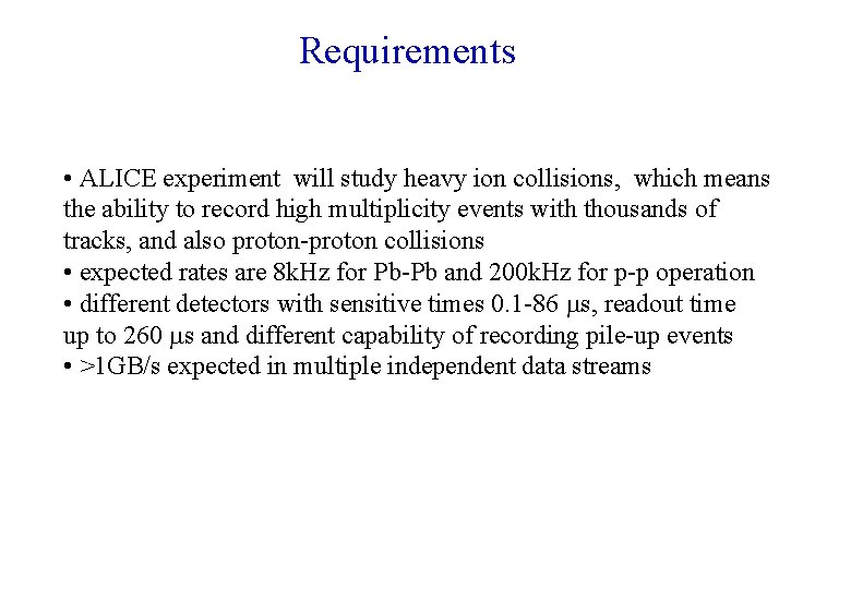
Requirements • ALICE experiment will study heavy ion collisions, which means the ability to record high multiplicity events with thousands of tracks, and also proton-proton collisions • expected rates are 8 k. Hz for Pb-Pb and 200 k. Hz for p-p operation • different detectors with sensitive times 0. 1 -86 s, readout time up to 260 s and different capability of recording pile-up events • >1 GB/s expected in multiple independent data streams

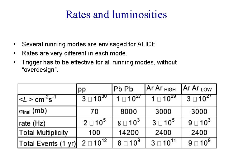
Rates and luminosities • Several running modes are envisaged for ALICE • Rates are very different in each mode. • Trigger has to be effective for all running modes, without “overdesign”.

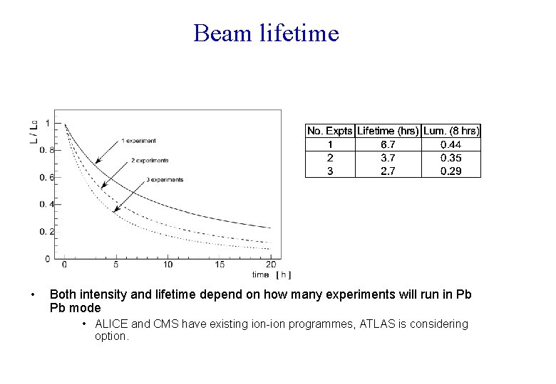
Beam lifetime • Both intensity and lifetime depend on how many experiments will run in Pb Pb mode • ALICE and CMS have existing ion-ion programmes, ATLAS is considering option.

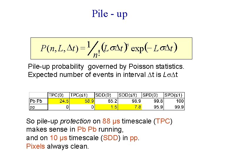
Pile - up P (n, L, Dt ) = 1 n n ( ) Ls. Dt exp(- Ls. Dt ) ! Pile-up probability governed by Poisson statistics. Expected number of events in interval Dt is Ls. Dt So pile-up protection on 88 μs timescale (TPC) makes sense in Pb Pb running, and on 10 μs timescale (SDD) in pp. Pixels always clean.

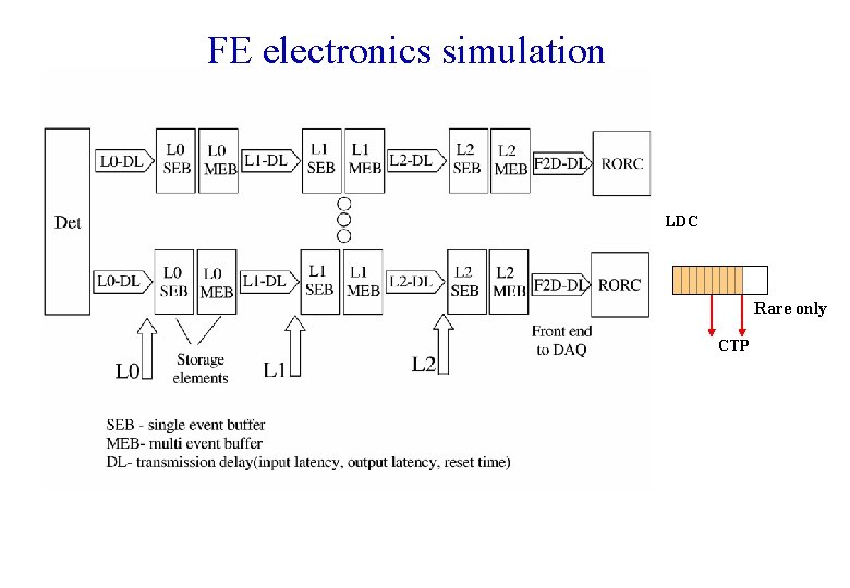
FE electronics simulation LDC Rare only CTP
![Rare events Events rejected due to Detector BUSY No All constraints Rare MU Rare events Events rejected due to Detector BUSY [%] No All constraints Rare MU](https://slidetodoc.com/presentation_image_h2/8ab822a75956351d25da580a50bcab40/image-7.jpg)
Rare events Events rejected due to Detector BUSY [%] No All constraints Rare MU 80 15 EL 95 55

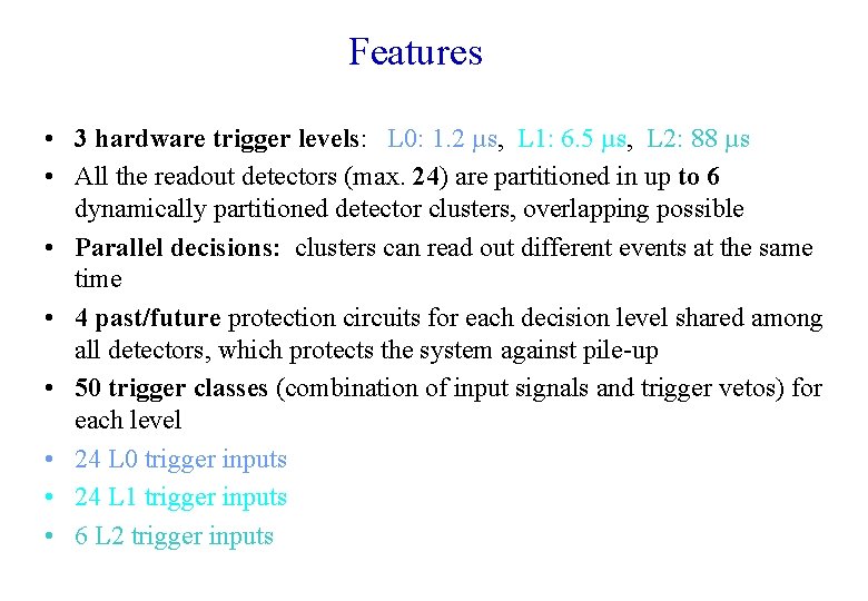
Features • 3 hardware trigger levels: L 0: 1. 2 µs, L 1: 6. 5 µs, L 2: 88 µs • All the readout detectors (max. 24) are partitioned in up to 6 dynamically partitioned detector clusters, overlapping possible • Parallel decisions: clusters can read out different events at the same time • 4 past/future protection circuits for each decision level shared among all detectors, which protects the system against pile-up • 50 trigger classes (combination of input signals and trigger vetos) for each level • 24 L 0 trigger inputs • 24 L 1 trigger inputs • 6 L 2 trigger inputs

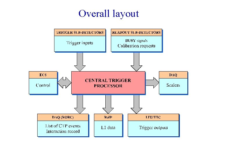
Overall layout

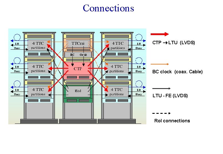
Connections CTP LTU (LVDS) BC clock (coax. Cable) LTU - FE (LVDS) Ro. I connections

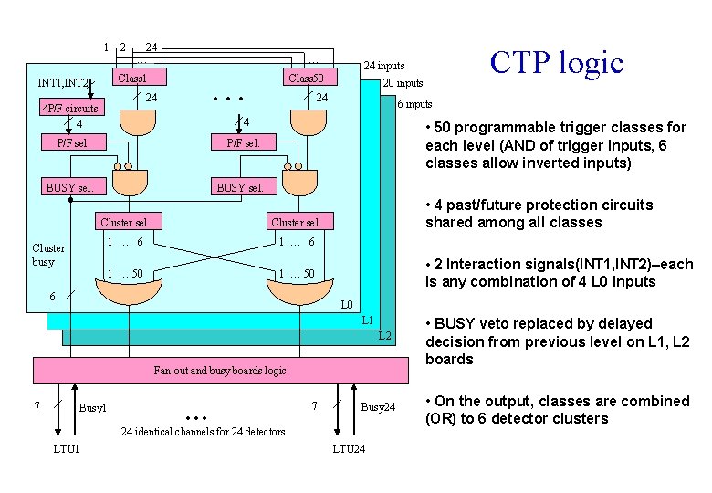
1 2 24 … … Class 1 INT 1, INT 2 Class 50 . . . 24 4 P/F circuits 4 20 inputs 24 6 inputs 4 P/F sel. • 50 programmable trigger classes for each level (AND of trigger inputs, 6 classes allow inverted inputs) P/F sel. BUSY sel. Cluster sel. 1 … 6 1 … 50 Cluster busy 6 • 4 past/future protection circuits shared among all classes • 2 Interaction signals(INT 1, INT 2)–each is any combination of 4 L 0 inputs L 0 L 1 L 2 Fan-out and busy boards logic 7 CTP logic 24 inputs Busy 1 … 7 Busy 24 24 identical channels for 24 detectors LTU 1 LTU 24 • BUSY veto replaced by delayed decision from previous level on L 1, L 2 boards • On the output, classes are combined (OR) to 6 detector clusters

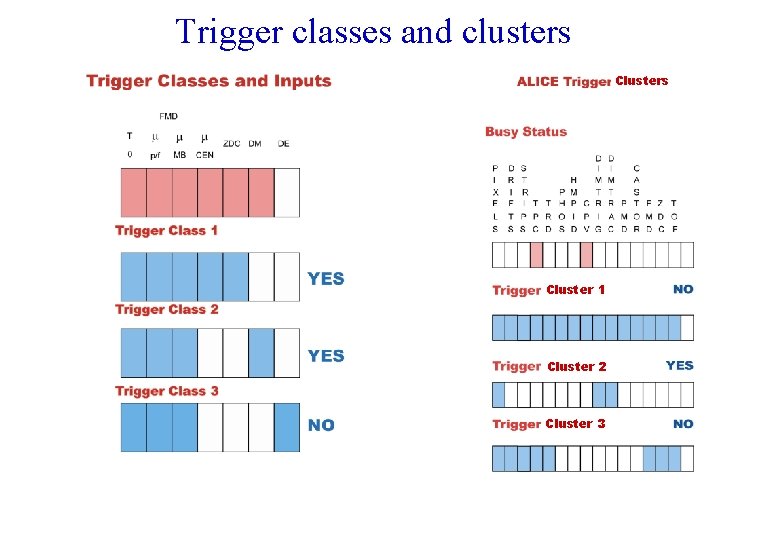
Trigger classes and clusters Cluster 1 Cluster 2 Cluster 3

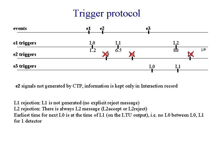
Trigger protocol events e 1 triggers e 2 triggers e 3 triggers e 1 L 0 1. 2 e 2 L 0 e 3 L 1 6. 5 L 2 88 L 1 L 0 L 2 s L 1 e 2 signals not generated by CTP, information is kept only in Interaction record L 1 rejection: L 1 is not generated (no explicit reject message) L 2 rejection: There is always L 2 message (L 2 accept or L 2 reject) Earliest time for next L 0 is at the time of L 1 (on the LTU output), i. e. no L 0 between L 0, L 1 for 1 detector

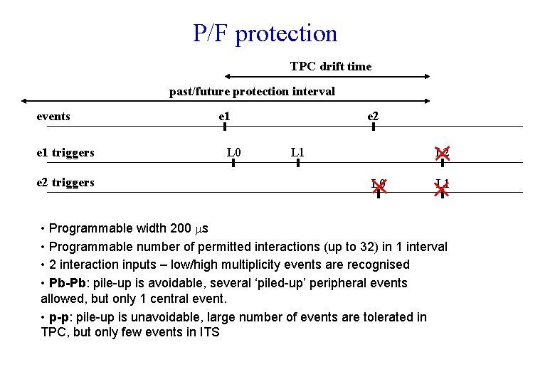
P/F protection TPC drift time past/future protection interval events e 1 triggers e 2 triggers e 1 L 0 e 2 L 1 L 2 L 0 L 1 • Programmable width 200 s • Programmable number of permitted interactions (up to 32) in 1 interval • 2 interaction inputs – low/high multiplicity events are recognised • Pb-Pb: pile-up is avoidable, several ‘piled-up’ peripheral events allowed, but only 1 central event. • p-p: pile-up is unavoidable, large number of events are tolerated in TPC, but only few events in ITS

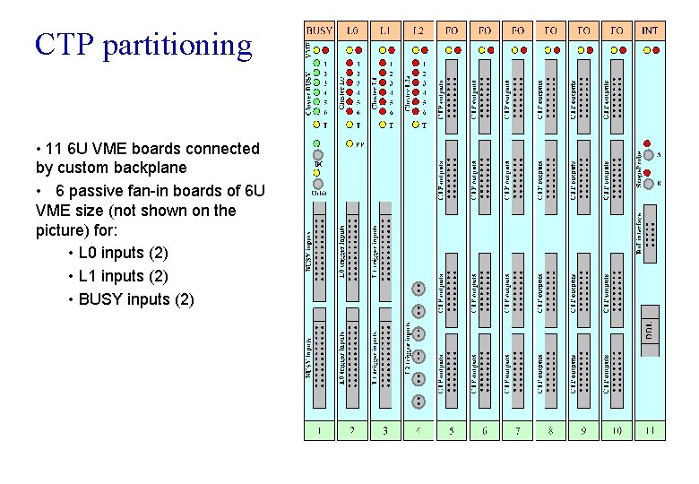
CTP partitioning • 11 6 U VME boards connected by custom backplane • 6 passive fan-in boards of 6 U VME size (not shown on the picture) for: • L 0 inputs (2) • L 1 inputs (2) • BUSY inputs (2)

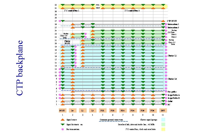
SCL 32 SDT 31 2 2 I C control bus 1 30 I C control bus 2 29 28 27 CTP BUSY 26 Interaction 1 25 Interaction 2 Strobe 24 23 CTP backplane 22 L 2 Data Strobe Data 1 Data 2 Class L 0 Data 21 Strobe Cluster BUSY 20 Class L 1 Data 19 18 17 Cluster L 1 16 15 14 13 12 11 10 9 Cluster L 0 8 7 6 5 Pre -pulse 4 Scope. Probe A 3 Scope. Probe B 2 Orbit 1 BC BUSY 1 L 0 L 1 L 2 FO 1 FO 2 FO 3 FO 4 FO 5 FO 6 INT 2 3 4 5 6 7 8 9 10 11 Signal source Signal destinati on Bus termination Common ground connection Cluster signal groups Serialised link, data and strobe line, 40 MHz 2 I C control bus, clock and serial data

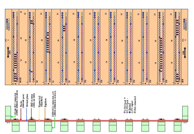
LVDS pair + LVDS pair Ground I 2 C signal Not connected (CERN, SCEM 09. 61. 33. 610. 3) DIN 41612 connector, a+c Rigidiser (50µm thick) Kapton foil (100Ω, size 0603) SMD resistor Ground plane (100Ω diff. pairs) Tracks (CERN, SCEM 09. 55. 05. 609. 6) 10 -pin IDC connector FO 1 L 2 FO INT 1 C A FO 1 C A C A L 1 1 L 0 1 BUSY 1 C A C A C A 10 10 10 GND I 2 C 2 20 20 20 I 2 C 1 1 1 32 32 32

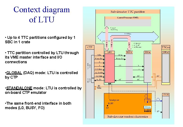
Context diagram of LTU • Up to 4 TTC partitions configured by 1 SBC in 1 crate • TTC partition controlled by LTU through its VME master interface and I/O connections • GLOBAL (DAQ) mode: LTU is controlled by CTP • STANDALONE mode: LTU is controlled by on-board CTP emulator • The same front-end interface in both modes (L 0, BUSY, FO)

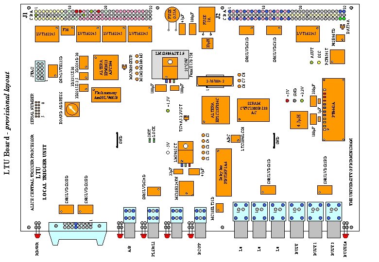
BUSY/L 0 1 THE UNIVERSITY OF BIRMINGHAM SN 65 LVDS 32 BD 100μF 1μF PT 6441 A 4. 7μH 330μF +3. 3 V GND +5 V C 6 C 7 C 8 PCF 8591 T OSC AOUT J 1 32 20 10 1 CBA J 2 FUSE 7 A 100μF 47μF 32 20 10 1 FUSE O. 75 A CBA BAT 54 A P 82 B 96 TD SN 65 LVDS 31 D 10μH LVT 162245 BUSY 2 1 GND 1 21°C/W Farnell 170 -758 LVT 162245 BUSY 1 1 1 LTC 1096 LCS 8 ADC ALTERA EP 1 C 12 F 324 C SSRAM CY 7 C 1382 B-133 AC BUSY L 0 SN 65 LVDS 31 D Delay line PDU 15 F-1 A 4 C 1 C 2 C 3 C 4 C 5 100μF 2 -767004 -2 1 1 MC 10 ELT 21 D 47μF TC 74 A 5 -3. 3 VCT M 1 M 2 M 3 M 4 M 5 MAX 809 SEUR LMS 1585 AIT-1. 5 L 0 BC/PP LM 7905 CT +1. 5 V 100μF Flash memory Am 29 LV 081 B MC 10 H 124 FN -5 V INIT LOCK GND ALTERA EPM 3512 AFC 256 3 D 3215 Z-30 3 D 3215 Z-2. 5 3 D 3314 D-30 SN 74 LVTH 125 D 1 LVT 162245 22μF SN 65 LVDS 34 D SN 65 LVDS 32 BD 0 BOARD ADDRESS 5 JTAG LVT 162245 PLSR/L 1 1 SN 65 LVDS 32 BD LOCAL TRIGGER UNIT LTU SERIAL NUMBER F 38 A/B RD/WR ALICE CENTRAL TRIGGER PROCESSOR LTU Board - provisional layout LVT 162245

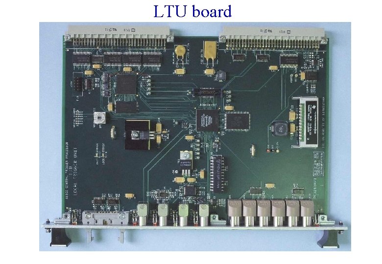
LTU board

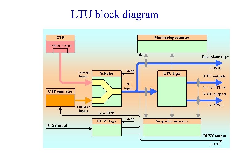
LTU block diagram

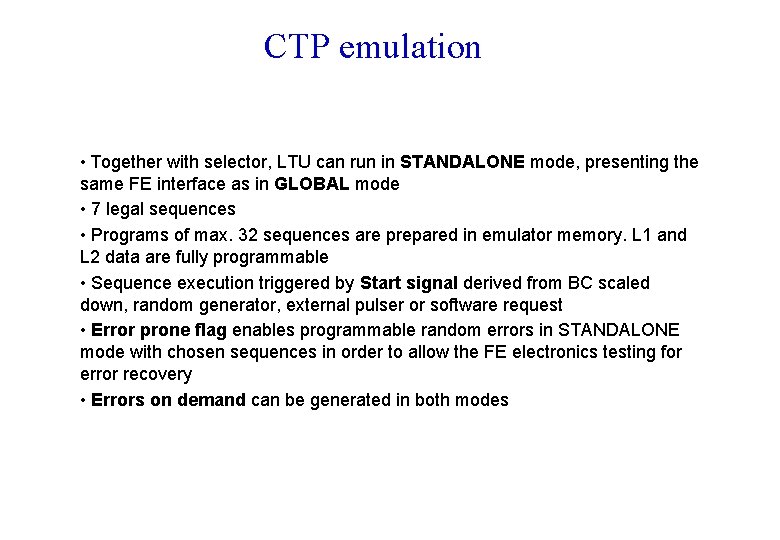
CTP emulation • Together with selector, LTU can run in STANDALONE mode, presenting the same FE interface as in GLOBAL mode • 7 legal sequences • Programs of max. 32 sequences are prepared in emulator memory. L 1 and L 2 data are fully programmable • Sequence execution triggered by Start signal derived from BC scaled down, random generator, external pulser or software request • Error prone flag enables programmable random errors in STANDALONE mode with chosen sequences in order to allow the FE electronics testing for error recovery • Errors on demand can be generated in both modes

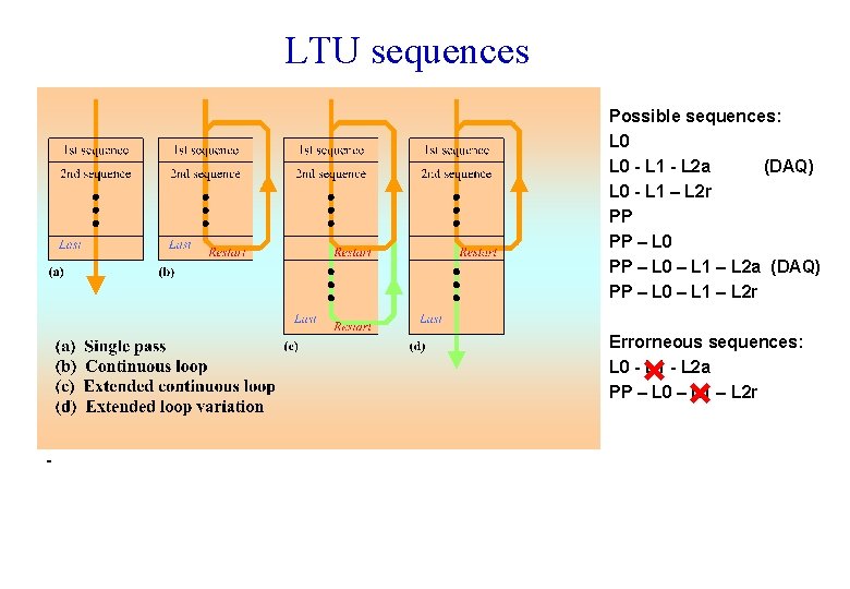
LTU sequences Possible sequences: L 0 - L 1 - L 2 a (DAQ) L 0 - L 1 – L 2 r PP PP – L 0 – L 1 – L 2 a (DAQ) PP – L 0 – L 1 – L 2 r Errorneous sequences: L 0 - L 1 - L 2 a PP – L 0 – L 1 – L 2 r -

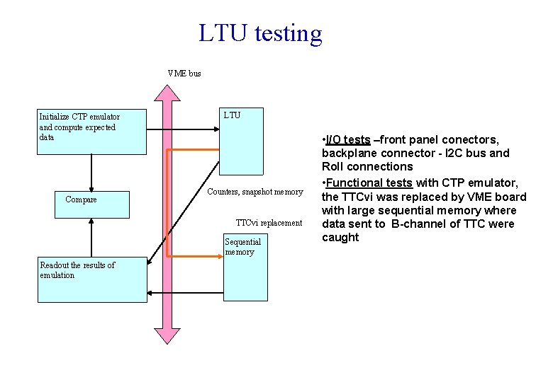
LTU testing VME bus Initialize CTP emulator and compute expected data Compare LTU Counters, snapshot memory TTCvi replacement Sequential memory Readout the results of emulation • I/O tests –front panel conectors, backplane connector - I 2 C bus and Ro. II connections • Functional tests with CTP emulator, the TTCvi was replaced by VME board with large sequential memory where data sent to B-channel of TTC were caught

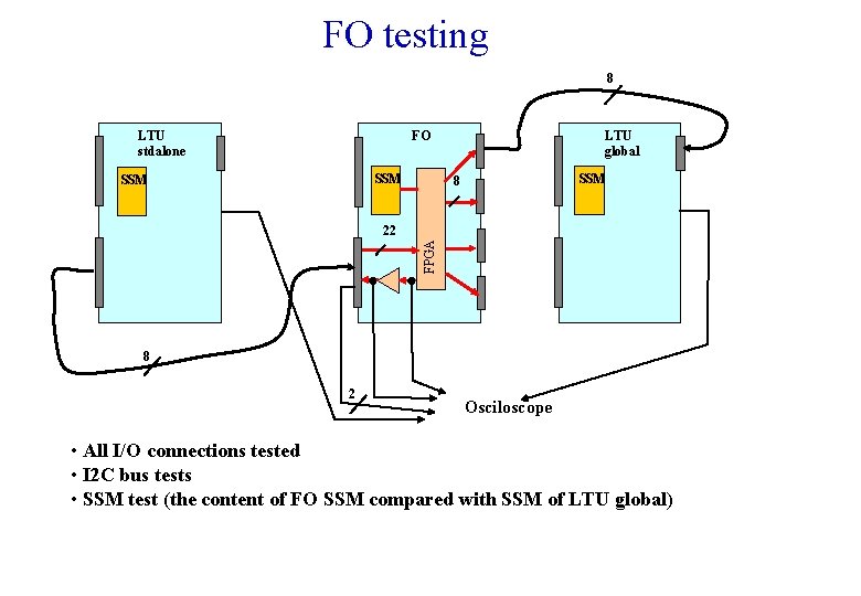
FO testing 8 LTU stdalone LTU global FO SSM SSM 8 FPGA 22 8 2 Osciloscope • All I/O connections tested • I 2 C bus tests • SSM test (the content of FO SSM compared with SSM of LTU global)

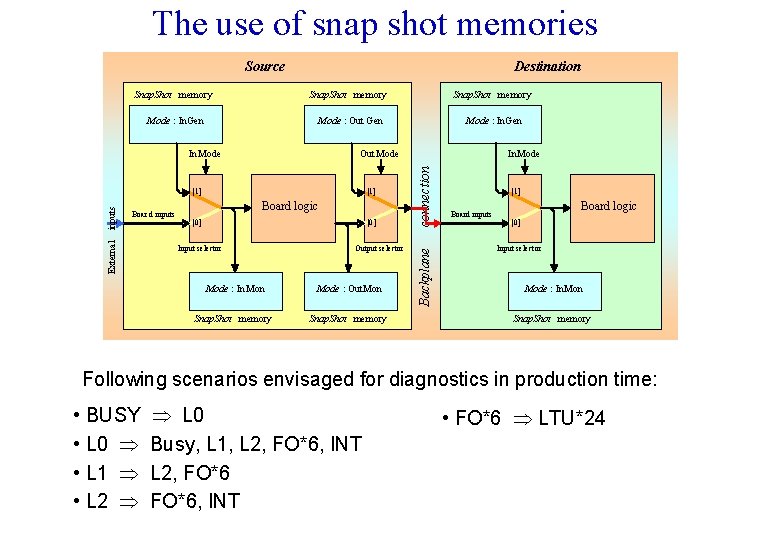
The use of snap shot memories Source Destination Snap. Shot memory Mode : In. Gen Mode : Out Gen Mode : In. Gen Boar d inputs External inputs [1] Board logic [0] Input selector Output selector Mode : In Mode : Out. Mon Snap. Shot memory In. Mode connection Out Mode Backplane In. Mode [1] Board inputs Board logic [0] Input selector Mode : In. Mon Snap. Shot memory Following scenarios envisaged for diagnostics in production time: • BUSY • L 0 • L 1 • L 2 L 0 Busy, L 1, L 2, FO*6, INT • FO*6 LTU*24

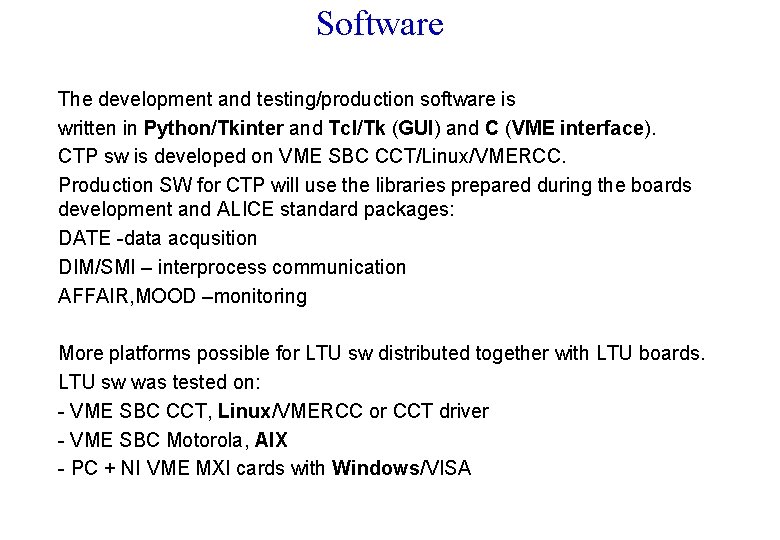
Software The development and testing/production software is written in Python/Tkinter and Tcl/Tk (GUI) and C (VME interface). CTP sw is developed on VME SBC CCT/Linux/VMERCC. Production SW for CTP will use the libraries prepared during the boards development and ALICE standard packages: DATE -data acqusition DIM/SMI – interprocess communication AFFAIR, MOOD –monitoring More platforms possible for LTU sw distributed together with LTU boards. LTU sw was tested on: - VME SBC CCT, Linux/VMERCC or CCT driver - VME SBC Motorola, AIX - PC + NI VME MXI cards with Windows/VISA

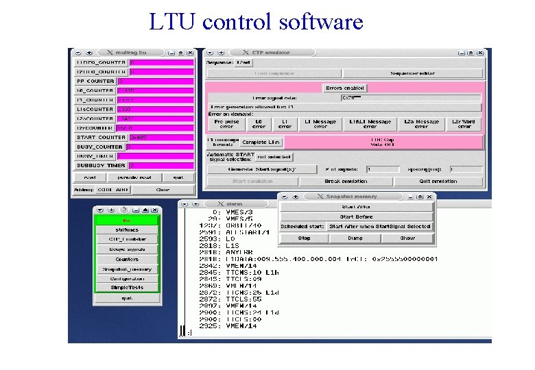
LTU control software

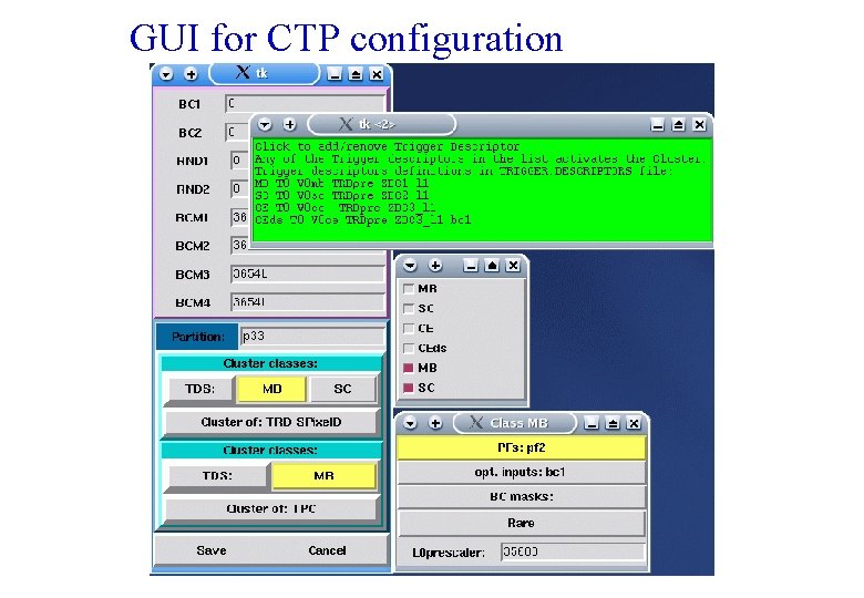
GUI for CTP configuration

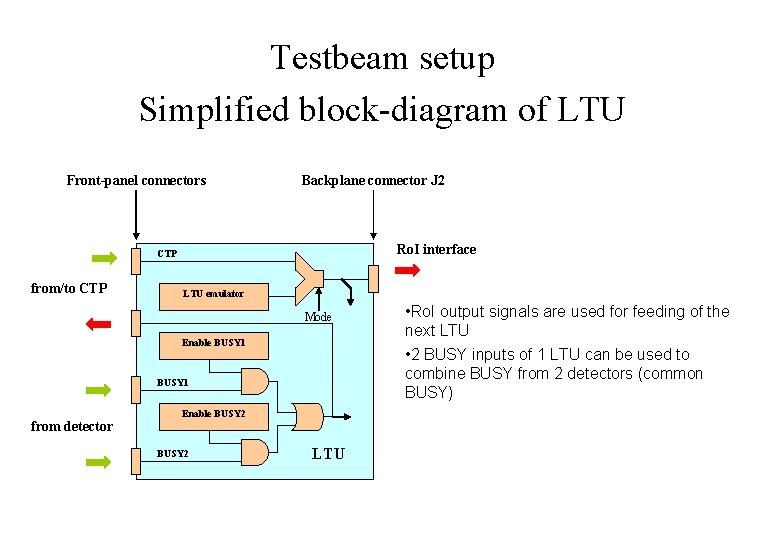
Testbeam setup Simplified block-diagram of LTU Front-panel connectors Backplane connector J 2 Ro. I interface CTP from/to CTP LTU emulator Mode Enable BUSY 1 from detector Enable BUSY 2 LTU • Ro. I output signals are used for feeding of the next LTU • 2 BUSY inputs of 1 LTU can be used to combine BUSY from 2 detectors (common BUSY)

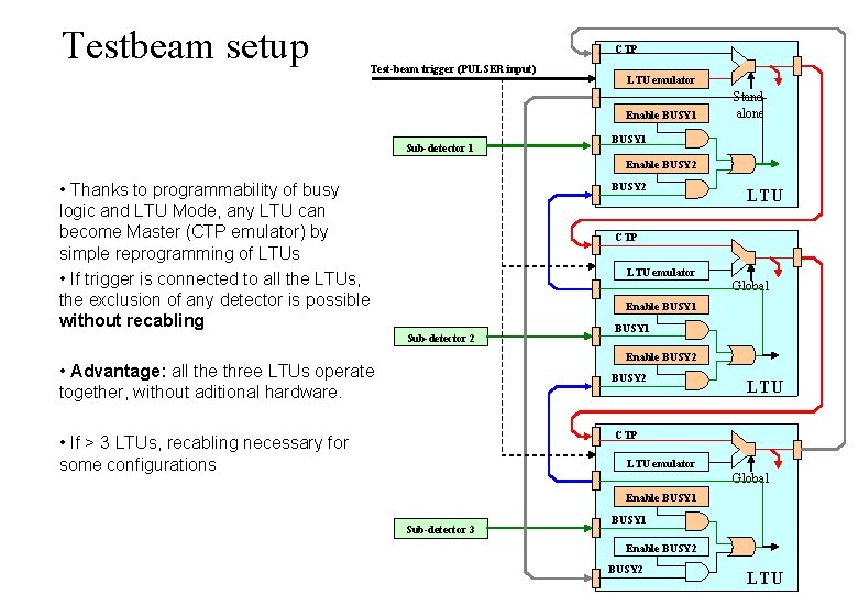
Testbeam setup CTP Test-beam trigger (PULSER input) LTU emulator Enable BUSY 1 Sub-detector 1 Standalone BUSY 1 Enable BUSY 2 • Thanks to programmability of busy logic and LTU Mode, any LTU can become Master (CTP emulator) by simple reprogramming of LTUs • If trigger is connected to all the LTUs, the exclusion of any detector is possible without recabling BUSY 2 LTU CTP LTU emulator Global Enable BUSY 1 Sub-detector 2 BUSY 1 Enable BUSY 2 • Advantage: all the three LTUs operate together, without aditional hardware. BUSY 2 LTU CTP • If > 3 LTUs, recabling necessary for some configurations LTU emulator Global Enable BUSY 1 Sub-detector 3 BUSY 1 Enable BUSY 2 LTU

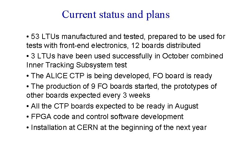
Current status and plans • 53 LTUs manufactured and tested, prepared to be used for tests with front-end electronics, 12 boards distributed • 3 LTUs have been used successfully in October combined Inner Tracking Subsystem test • The ALICE CTP is being developed, FO board is ready • The production of 9 FO boards started, the prototypes of other boards expected every 3 weeks • All the CTP boards expected to be ready in August • FPGA code and control software development • Installation at CERN at the beginning of the next year