ALICE ITS Readout Firmware Overview ITS Readout Electronic
- Slides: 22

ALICE ITS Readout Firmware Overview ITS Readout Electronic – Engineering Design Review – 27 Jan 2017 – CERN

Overview ALICE ITS UPGRADE 2

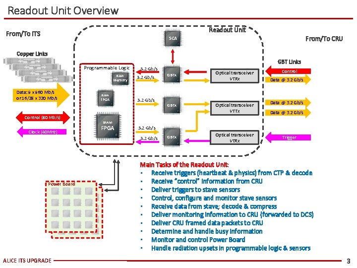
Readout Unit Overview Readout Unit From/To ITS From/To CRU SCA Copper Links Programmable Logic FLASH Memory FLASH GBT Links 3. 2 Gb/s GBTx Optical transceiver VTRx Control Data @ 3. 2 Gb/s Memory Data: 9 x 960 Mb/s or 16/28 x 320 Mb/s Control (80 Mb/s) Clock (40 MHz) FLASH FPGA 3. 2 Gb/s ALICE ITS UPGRADE Optical transceiver VTTx Data @ 3. 2 Gb/s SRAM FPGA 3. 2 Gb/s Power Board Power Unit (PU) GBTx Optical transceiver VTRx Trigger Main Tasks of the Readout Unit: • Receive triggers (heartbeat & physics) from CTP & decode • Receive “control” information from CRU • Deliver triggers to stave sensors • Control, configure and monitor stave sensors • Receive data from stave; decode & compress • Deliver monitoring information to CRU (forwarded to DCS) • Deliver CRU framed data packets to CRU • Determine and handle busy information • Monitor and control Power Board • Handle radiation upsets in programmable logic & sensors 3

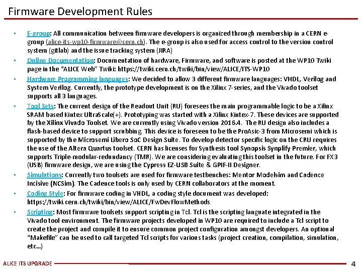
Firmware Development Rules • • E-group: All communication between firmware developers is organized through membership in a CERN egroup (alice-its-wp 10 -firmware@cern. ch). The e-group is also used for access control to the version control system (gitlab) and the issue tracking system (JIRA) Online Documentation: Documentation of hardware, Firmware, and software is posted at the WP 10 Twiki page in the “ALICE Web” Twiki: https: //twiki. cern. ch/twiki/bin/view/ALICE/ITS-WP 10 Hardware Programming languages: We decided to allow 3 different firmware languages: VHDL, Verilog and System Verilog. Currently, the prototype development is on the Xilinx 7 -series, and the Vivado toolset supports all 3 languages. Tool Sets: The current design of the Readout Unit (RU) foresees the main programmable logic to be a Xilinx SRAM based Kintex Ultra. Scale(+). Prototyping was started with a Xilinx Kintex-7. These devices are supported by the Xilinx Vivado Toolset. We are currently using Vivado version 2016. 4. The RU design also includes a flash-based device to support scrubbing. This device is foreseen to be the Pro. Asic-3 from Microsemi which is supported by the Microsemi Libero So. C Design Suite. To develop detector specific logic on the CRU requires the use of the Altera Quartus toolset. CERN has licenses for Synthesis tool Synopsis Synplify Premier, which supports Triple-modular-redundancy (TMR). We are considering evaluating this toolset in the future. For FX 3 (USB) firmware design, we are using the Cypress EZ-USB Suite & GPIF-II Designer. Simulations: Currently two toolsets are used for firmware testbenches: Mentor Modelsim and Cadence Incisive (NCSim). The Cadence tools is only used by CERN collaborators at the moment. Coding Style: For firmware coding in VHDL, a coding style document was developed: https: //twiki. cern. ch/twiki/bin/view/ALICE/Fw. Dev. Flow. Methods Scripting: Most firmware toolsets support scripting in Tcl is the scripting languate integrated in the Vivado tool environment. The firmware projects developed in WP 10 are required to include a Tcl script to create the project and compile it to ensure common project configuration amongst developers. An optional “Makefile” can be used to call targeted Tcl scripts for various tasks (project creation, compilation, simulation, etc…) ALICE ITS UPGRADE 4

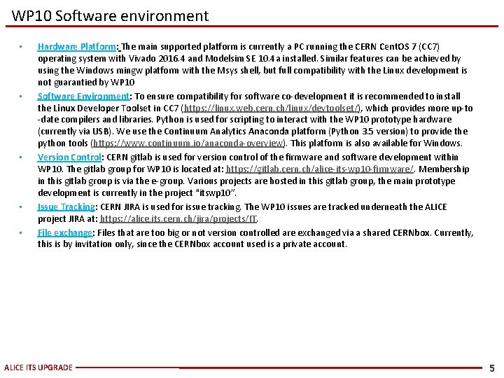
WP 10 Software environment • • • Hardware Platform: The main supported platform is currently a PC running the CERN Cent. OS 7 (CC 7) operating system with Vivado 2016. 4 and Modelsim SE 10. 4 a installed. Similar features can be achieved by using the Windows mingw platform with the Msys shell, but full compatibility with the Linux development is not guarantied by WP 10 Software Environment: To ensure compatibility for software co-development it is recommended to install the Linux Developer Toolset in CC 7 (https: //linux. web. cern. ch/linux/devtoolset/), which provides more up-to -date compilers and libraries. Python is used for scripting to interact with the WP 10 prototype hardware (currently via USB). We use the Continuum Analytics Anaconda platform (Python 3. 5 version) to provide the python tools (https: //www. continuum. io/anaconda-overview). This platform is also available for Windows. Version Control: CERN gitlab is used for version control of the firmware and software development within WP 10. The gitlab group for WP 10 is located at: https: //gitlab. cern. ch/alice-its-wp 10 -firmware/. Membership in this gitlab group is via the e-group. Various projects are hosted in this gitlab group, the main prototype development is currently in the project “itswp 10”. Issue Tracking: CERN JIRA is used for issue tracking. The WP 10 issues are tracked underneath the ALICE project JIRA at: https: //alice. its. cern. ch/jira/projects/IT. File exchange: Files that are too big or not version controlled are exchanged via a shared CERNbox. Currently, this is by invitation only, since the CERNbox account used is a private account. ALICE ITS UPGRADE 5

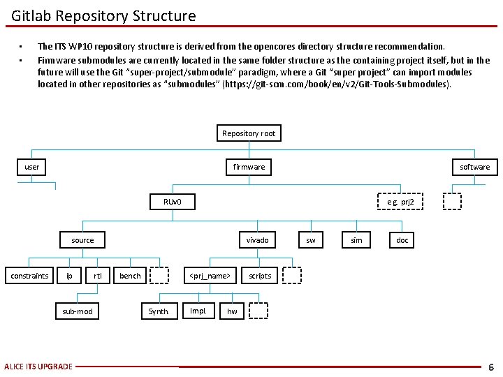
Gitlab Repository Structure • • The ITS WP 10 repository structure is derived from the opencores directory structure recommendation. Firmware submodules are currently located in the same folder structure as the containing project itself, but in the future will use the Git “super-project/submodule” paradigm, where a Git “super project” can import modules located in other repositories as “submodules” (https: //git-scm. com/book/en/v 2/Git-Tools-Submodules). Repository root user firmware software e. g. prj 2 RUv 0 source constraints ip sub-mod ALICE ITS UPGRADE rtl vivado bench <prj_name> Synth. Impl. sw sim doc scripts hw 6

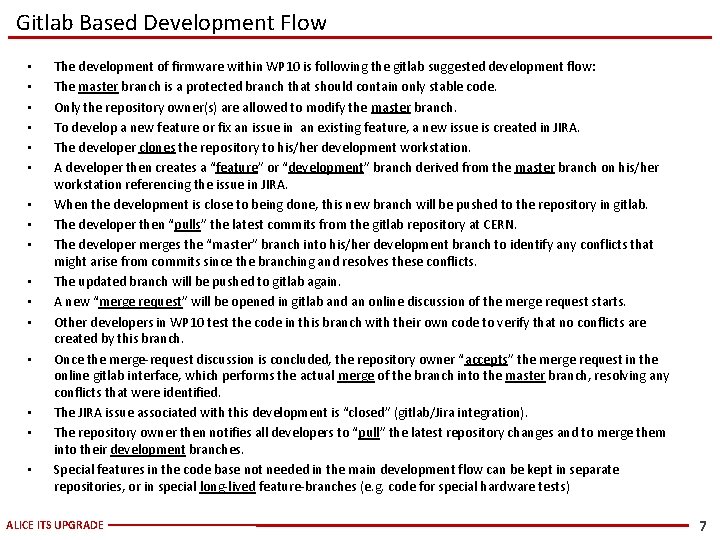
Gitlab Based Development Flow • • • • The development of firmware within WP 10 is following the gitlab suggested development flow: The master branch is a protected branch that should contain only stable code. Only the repository owner(s) are allowed to modify the master branch. To develop a new feature or fix an issue in an existing feature, a new issue is created in JIRA. The developer clones the repository to his/her development workstation. A developer then creates a “feature” or “development” branch derived from the master branch on his/her workstation referencing the issue in JIRA. When the development is close to being done, this new branch will be pushed to the repository in gitlab. The developer then “pulls” the latest commits from the gitlab repository at CERN. The developer merges the “master” branch into his/her development branch to identify any conflicts that might arise from commits since the branching and resolves these conflicts. The updated branch will be pushed to gitlab again. A new “merge request” will be opened in gitlab and an online discussion of the merge request starts. Other developers in WP 10 test the code in this branch with their own code to verify that no conflicts are created by this branch. Once the merge-request discussion is concluded, the repository owner “accepts” the merge request in the online gitlab interface, which performs the actual merge of the branch into the master branch, resolving any conflicts that were identified. The JIRA issue associated with this development is “closed” (gitlab/Jira integration). The repository owner then notifies all developers to “pull” the latest repository changes and to merge them into their development branches. Special features in the code base not needed in the main development flow can be kept in separate repositories, or in special long-lived feature-branches (e. g. code for special hardware tests) ALICE ITS UPGRADE 7

Firmware Structure ALICE ITS UPGRADE 8

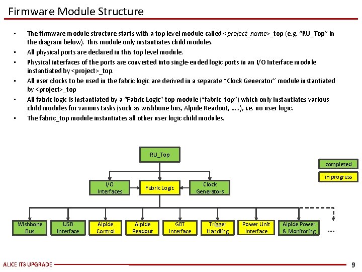
Firmware Module Structure • • • The firmware module structure starts with a top level module called <project_name>_top (e. g. “RU_Top” in the diagram below). This module only instantiates child modules. All physical ports are declared in this top level module. Physical interfaces of the ports are converted into single-ended logic ports in an I/O Interface module instantiated by <project>_top. All user clocks to be used in the fabric logic are derived in a separate “Clock Generator” module instantiated by <project>_top All fabric logic is instantiated by a “Fabric Logic” top module (“fabric_top”) which only instantiates various child modules for various tasks (such as wishbone bus, Alpide Readout, …. . ), i. e. no user logic. The fabric_top module instantiates all other user logic child modules. RU_Top completed I/O Interfaces Wishbone Bus ALICE ITS UPGRADE USB Interface Alpide Control Fabric Logic Alpide Readout GBT Interface in progress Clock Generators Trigger Handling Power Unit Interface Alpide Power & Monitoring … 9

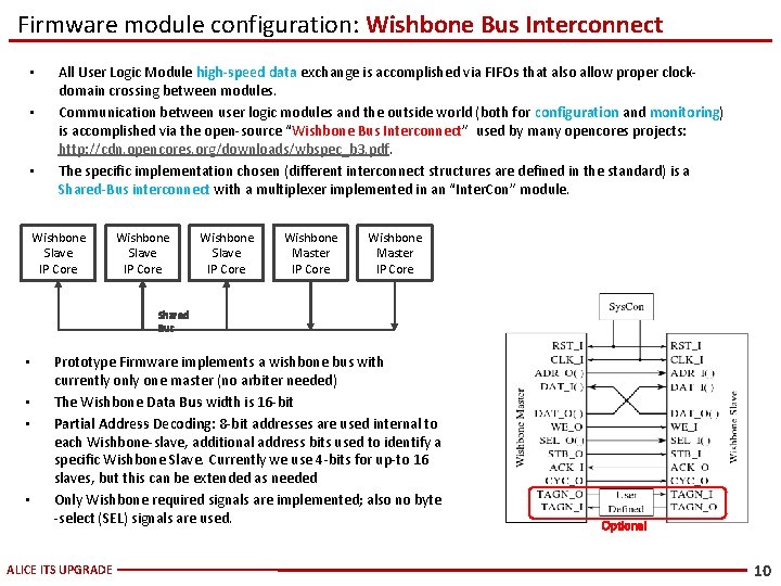
Firmware module configuration: Wishbone Bus Interconnect • • • All User Logic Module high-speed data exchange is accomplished via FIFOs that also allow proper clockdomain crossing between modules. Communication between user logic modules and the outside world (both for configuration and monitoring) is accomplished via the open-source “Wishbone Bus Interconnect” used by many opencores projects: http: //cdn. opencores. org/downloads/wbspec_b 3. pdf. The specific implementation chosen (different interconnect structures are defined in the standard) is a Shared-Bus interconnect with a multiplexer implemented in an “Inter. Con” module. Wishbone Slave IP Core Wishbone Master IP Core Shared Bus • • Prototype Firmware implements a wishbone bus with currently one master (no arbiter needed) The Wishbone Data Bus width is 16 -bit Partial Address Decoding: 8 -bit addresses are used internal to each Wishbone-slave, additional address bits used to identify a specific Wishbone Slave. Currently we use 4 -bits for up-to 16 slaves, but this can be extended as needed Only Wishbone required signals are implemented; also no byte -select (SEL) signals are used. ALICE ITS UPGRADE Optional 10

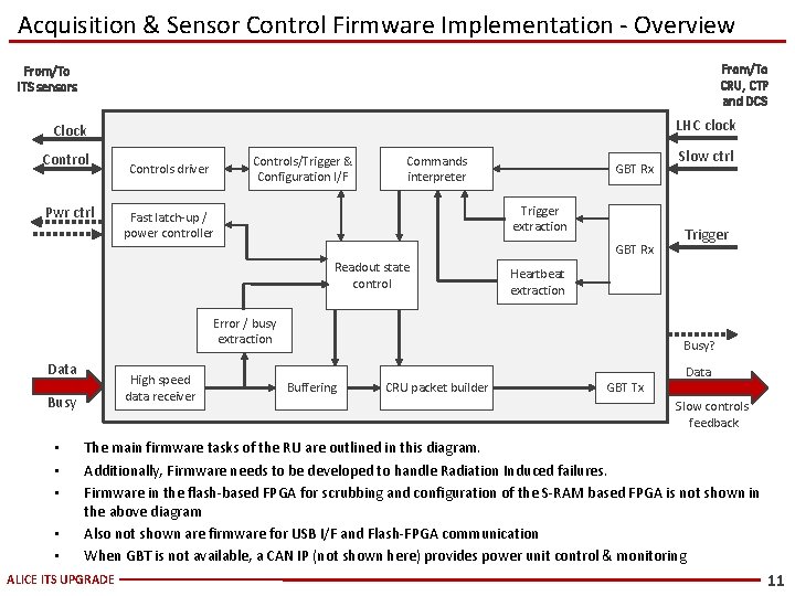
Acquisition & Sensor Control Firmware Implementation - Overview From/To CRU, CTP and DCS From/To ITS sensors LHC clock Control Pwr ctrl Controls/Trigger & Configuration I/F Controls driver Commands interpreter GBT Rx Trigger extraction Fast latch-up / power controller GBT Rx Readout state control High speed data receiver Busy • • • Trigger Heartbeat extraction Error / busy extraction Data Slow ctrl Busy? Buffering CRU packet builder GBT Tx Data Slow controls feedback The main firmware tasks of the RU are outlined in this diagram. Additionally, Firmware needs to be developed to handle Radiation Induced failures. Firmware in the flash-based FPGA for scrubbing and configuration of the S-RAM based FPGA is not shown in the above diagram Also not shown are firmware for USB I/F and Flash-FPGA communication When GBT is not available, a CAN IP (not shown here) provides power unit control & monitoring ALICE ITS UPGRADE 11

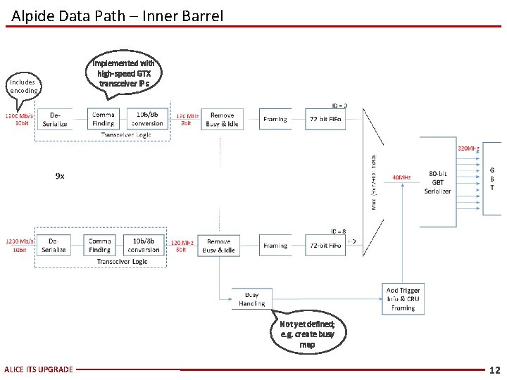
Alpide Data Path – Inner Barrel Includes encoding Implemented with high-speed GTX transceiver IPs Not yet defined; e. g. create busy map ALICE ITS UPGRADE 12

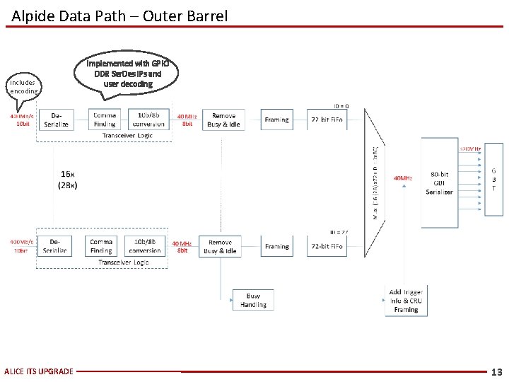
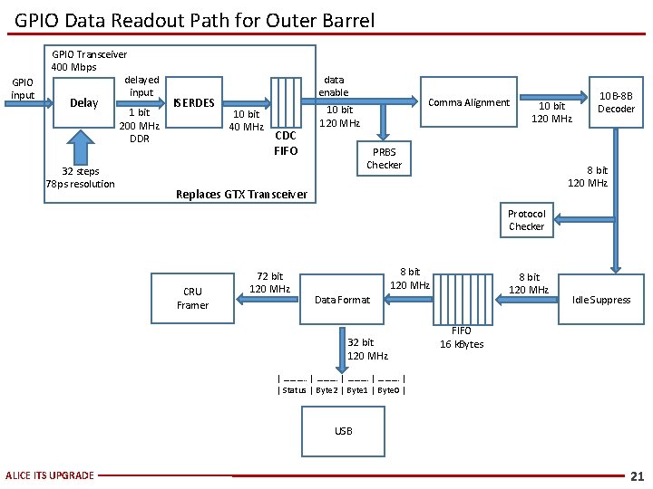
Alpide Data Path – Outer Barrel Includes encoding ALICE ITS UPGRADE Implemented with GPIO DDR Ser. Des IPs and user decoding 13

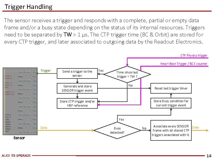
Trigger Handling The sensor receives a trigger and responds with a complete, partial or empty data frame and/or a busy state depending on the status of its internal resources. Triggers need to be separated by TW > 1 µs. The CTP trigger time (BC & Orbit) are stored for every CTP trigger, and later associated to outgoing data by the Readout Electronics. CTP Physics trigger Heart Beat Trigger / BCX counter Trigger Send a trigger to the sensor. Yes Time since last trigger > TW ? No Generate and store SENSOR trigger event Reset last trigger timer Store Busy condition for current trigger event Store CTP trigger and/or HBF reference Yes Data Sensor ALICE ITS UPGRADE Busy detected? No Associate every SENSOR Data frame with all stored CTP triggers associated with it. 14

Prototype Firmware Development ALICE ITS UPGRADE 15

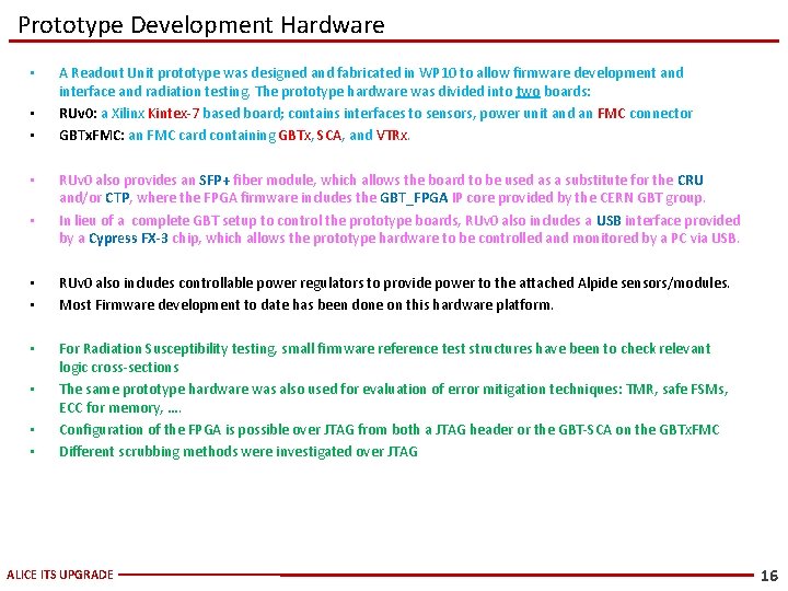
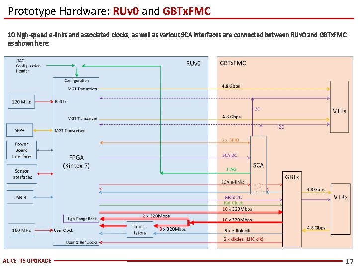
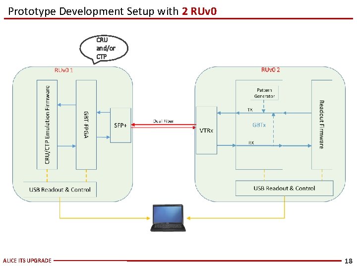
Prototype Development Hardware • • • A Readout Unit prototype was designed and fabricated in WP 10 to allow firmware development and interface and radiation testing. The prototype hardware was divided into two boards: RUv 0: a Xilinx Kintex-7 based board; contains interfaces to sensors, power unit and an FMC connector GBTx. FMC: an FMC card containing GBTx, SCA, and VTRx. RUv 0 also provides an SFP+ fiber module, which allows the board to be used as a substitute for the CRU and/or CTP, where the FPGA firmware includes the GBT_FPGA IP core provided by the CERN GBT group. In lieu of a complete GBT setup to control the prototype boards, RUv 0 also includes a USB interface provided by a Cypress FX-3 chip, which allows the prototype hardware to be controlled and monitored by a PC via USB. • • RUv 0 also includes controllable power regulators to provide power to the attached Alpide sensors/modules. Most Firmware development to date has been done on this hardware platform. • For Radiation Susceptibility testing, small firmware reference test structures have been to check relevant logic cross-sections The same prototype hardware was also used for evaluation of error mitigation techniques: TMR, safe FSMs, ECC for memory, …. Configuration of the FPGA is possible over JTAG from both a JTAG header or the GBT-SCA on the GBTx. FMC Different scrubbing methods were investigated over JTAG • • • ALICE ITS UPGRADE 16

Prototype Hardware: RUv 0 and GBTx. FMC 10 high-speed e-links and associated clocks, as well as various SCA interfaces are connected between RUv 0 and GBTx. FMC as shown here: ALICE ITS UPGRADE 17

Prototype Development Setup with 2 RUv 0 CRU and/or CTP ALICE ITS UPGRADE 18

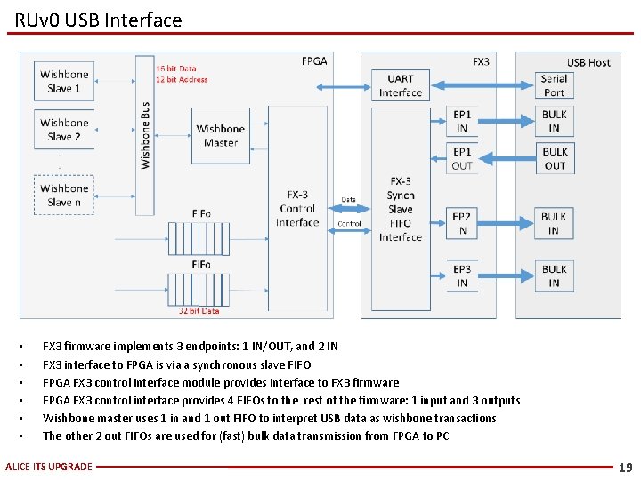
RUv 0 USB Interface • • • FX 3 firmware implements 3 endpoints: 1 IN/OUT, and 2 IN FX 3 interface to FPGA is via a synchronous slave FIFO FPGA FX 3 control interface module provides interface to FX 3 firmware FPGA FX 3 control interface provides 4 FIFOs to the rest of the firmware: 1 input and 3 outputs Wishbone master uses 1 in and 1 out FIFO to interpret USB data as wishbone transactions The other 2 out FIFOs are used for (fast) bulk data transmission from FPGA to PC ALICE ITS UPGRADE 19

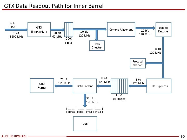
GTX Data Readout Path for Inner Barrel GTX Input 1 bit 1200 MHz GTX Transceiver 20 bit 60 MHz CDC FIFO Comma Alignment 10 bit 120 MHz PRBS Checker 10 B-8 B Decoder 8 bit 120 MHz Protocol Checker CRU Framer 72 bit 120 MHz 8 bit 120 MHz Data Format 32 bit 120 MHz Idle Suppress FIFO 16 k. Bytes | ………. | | Status | Byte 2 | Byte 1 | Byte 0 | USB ALICE ITS UPGRADE 20

GPIO Data Readout Path for Outer Barrel GPIO input GPIO Transceiver 400 Mbps delayed input Delay 32 steps 78 ps resolution 1 bit 200 MHz DDR ISERDES data enable 10 bit 40 MHz CDC FIFO Comma Alignment 10 bit 120 MHz PRBS Checker 10 B-8 B Decoder 8 bit 120 MHz Replaces GTX Transceiver Protocol Checker CRU Framer 72 bit 120 MHz 8 bit 120 MHz Data Format 32 bit 120 MHz Idle Suppress FIFO 16 k. Bytes | ………. | | Status | Byte 2 | Byte 1 | Byte 0 | USB ALICE ITS UPGRADE 21

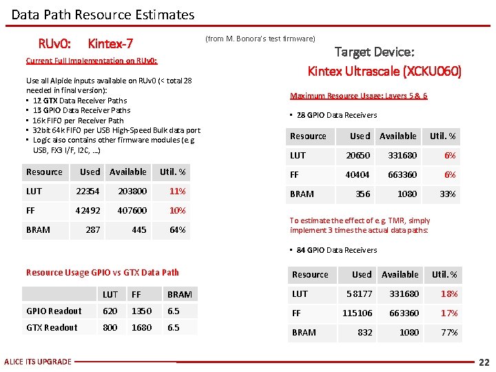
Data Path Resource Estimates RUv 0: (from M. Bonora’s test firmware) Kintex-7 Target Device: Kintex Ultrascale (XCKU 060) Current Full Implementation on RUv 0: Use all Alpide inputs available on RUv 0 (< total 28 needed in final version): • 12 GTX Data Receiver Paths • 13 GPIO Data Receiver Paths • 16 k FIFO per Receiver Path • 32 bit 64 k FIFO per USB High-Speed Bulk data port • Logic also contains other firmware modules (e. g. USB, FX 3 I/F, I 2 C, …) Resource Used Available Util. % LUT 22354 203800 11% FF 42492 407600 10% 287 445 64% BRAM Maximum Resource Usage: Layers 5 & 6 • 28 GPIO Data Receivers Resource Used Available Util. % LUT 20650 331680 6% FF 40404 663360 6% 356 1080 33% BRAM To estimate the effect of e. g. TMR, simply implement 3 times the actual data paths: • 84 GPIO Data Receivers Resource Usage GPIO vs GTX Data Path Resource LUT FF BRAM LUT GPIO Readout 620 1350 6. 5 FF GTX Readout 800 1680 6. 5 ALICE ITS UPGRADE BRAM Used Available Util. % 58177 331680 18% 115106 663360 17% 832 1080 77% 22