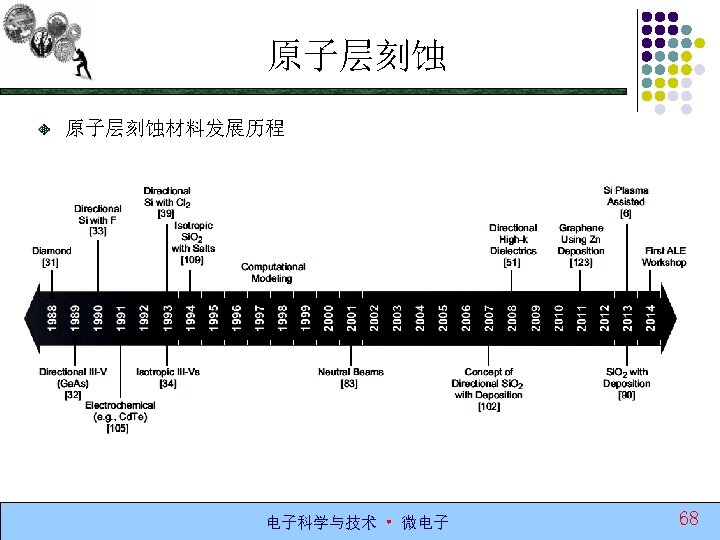
ALE Yoder in 1988 ALE of diamond films
 Yoder in 1988 ALE of diamond films; ALD -- reciprocity of the ALE.")

 hosted an inaugural ALE workshop; The second annual")
; 3. Digital")


 ;")


; 2. Saturation curve(饱和曲线) ;")


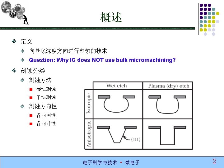
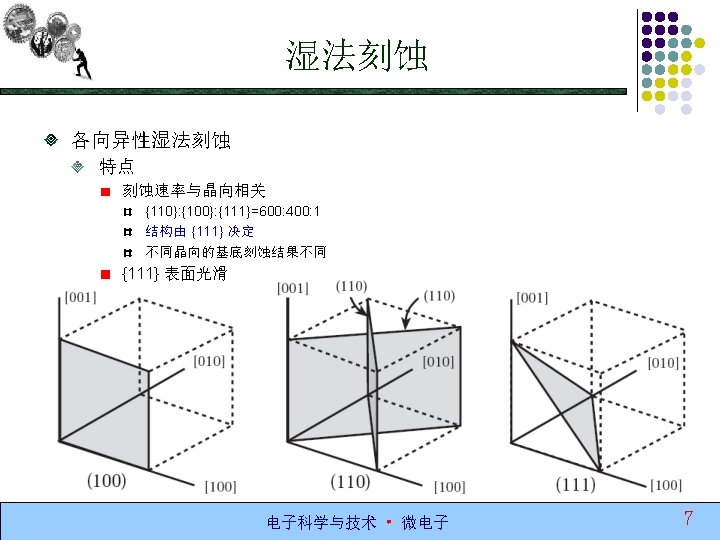
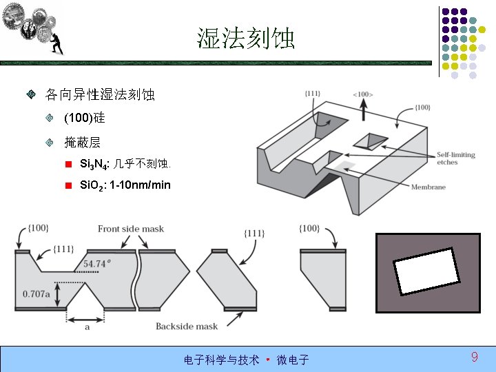
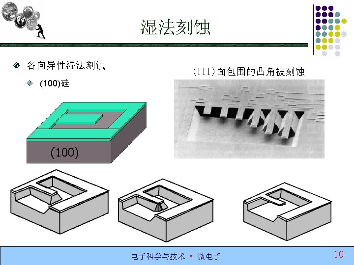
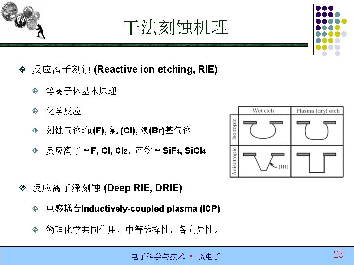
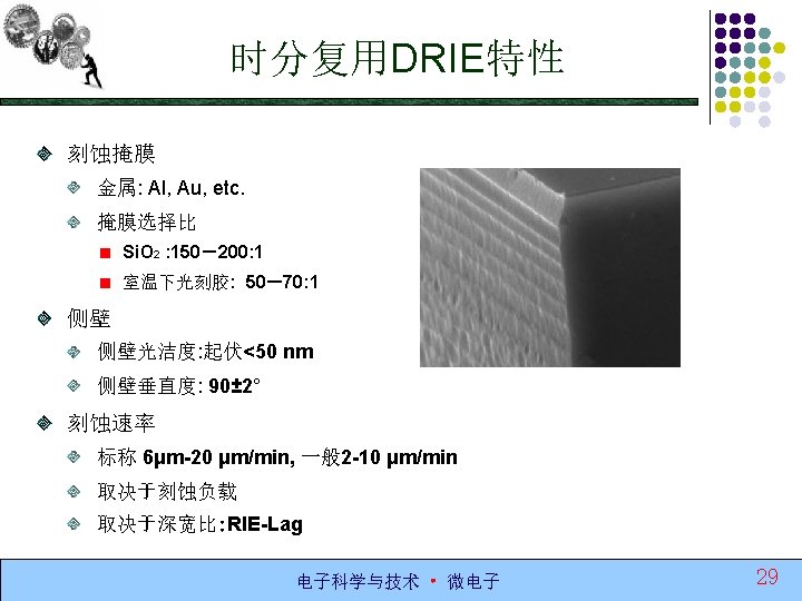
 Excellent depth uniformity across the wafer; (b) Flat silicon etch")


;")


; Plasma assistance;")


 High dielectric constant oxides ; Hafnium")


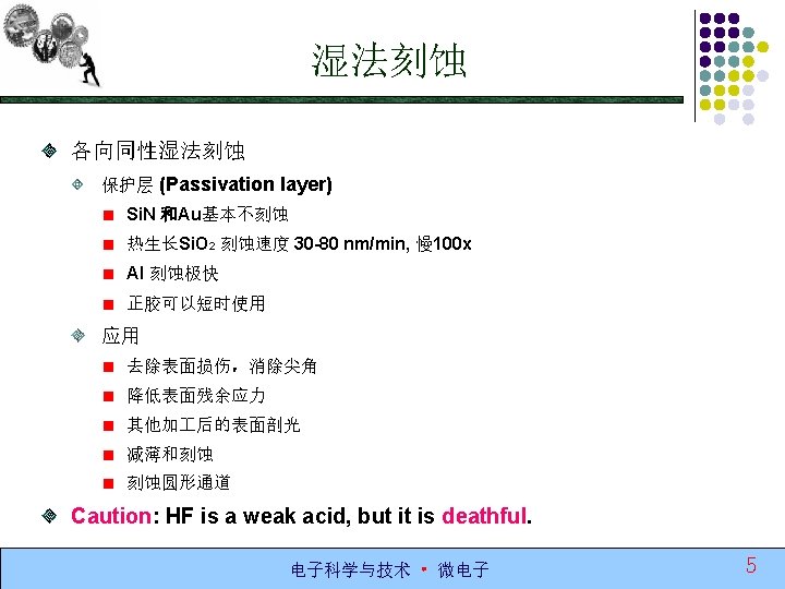
 Chlorinating the surface, immersion into dilute HCl bath to")


 1. Directional ALE approach Reaction A ,")
 “Extraction” category as the oxidation actually; Extracted")

- Slides: 83
原子层刻蚀(ALE) Yoder in 1988 ALE of diamond films; ALD -- reciprocity of the ALE. Maki and Ehrlich in 1989 Bilayer etching of Ga. As using chlorine chemisorptions. 电子科学与技术 • 微电子 34
History of原子层刻蚀 Silicon and Ga. As have been the most studied ALE materials in the 1990 s; Ga. As predominately ,Ga. As was the III–V material of focus for replacing silicon. ALE has been demonstrated on well over 20 materials: Elemental semiconductors; Compound semiconductors; Insulators; Metals, 电子科学与技术 • 微电子 35
History of原子层刻蚀 In April 2014, Sematech(美国半导体科技研发联盟) hosted an inaugural ALE workshop; The second annual ALE workshop is planned for 2015 in conjunction with the ALD conference in Portland. 电子科学与技术 • 微电子 36
History of原子层刻蚀 ALE的其他一些名字: 1. Atomic layer etching; 2. Plasma atomic layer etching(PALE); 3. Digital etching ; 4. Layer by layer etch ; 5. Molecular layer etching ; 6. Molecular bilayer etching; 7. Single layer etching; 8. Thin layer etching; 9. Monolayer chemical beam etching(ML-CBET); 10. Atomic layer removal. 电子科学与技术 • 微电子 37
原子层刻蚀 艺步骤 1. Starts with a modification step to form a reactive layer; 2. A removal step to take off only this modified layer; 3. Using ions allows for the directional etching required to form deep, narrow structures. 电子科学与技术 • 微电子 38
原子层刻蚀 Plasma etching has been represented by A+B: Reaction A, represents neutral reactions; Reaction B, represents energetic ions above an etching threshold. 电子科学与技术 • 微电子 39
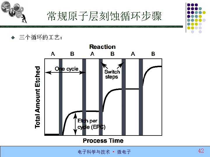
常规原子层刻蚀循环步骤 The simplest ALE consists of two sequential steps: Surface modification (reaction A) ; Removal (reaction B). Modification step Forms a thin reactive surface layer with a well-defined thickness ; More easily removed than the unmodified material; Characterized by a sharp gradient in chemical composition and/or physical structure of the outermost layer of a material. 电子科学与技术 • 微电子 40
常规原子层刻蚀循环步骤 The removal step Takes away the modified layer while keeping the underlying substrate intact; “Resetting” the surface to a pristine or near-pristine state for the next etching cycle; The total amount of material removed is determined by the repeated cycles。 电子科学与技术 • 微电子 41
原子层刻蚀 The general ALE concept applies to a wide variety of etching schemes: Directional or isotropic; Selective or nonselective; Reactants delivered by gases, plasma, wet (liquid) chemistry, or other sources. All schemes share the same defining ALE criteria: 1. Separation into a sequence (cycling) of independent unit process reactions; 2. At least one step is as Self-limiting as possible. 电子科学与技术 • 微电子 43
原子层刻蚀 Separation of reactions means: 1. The composite process runs as a repeated series of two or more independent unit steps; 2. With each step designed to be as simple as possible. In plasma etching Each step with distinct chemistry, speciation, and plasma energy composition. The separation is either temporal or spatial, Time domain is most common using a single chamber with sophisticated process control technology to modulate process parameters; Such as gas composition, gas flow, pressure, and plasma power. 电子科学与技术 • 微电子 44
原子层刻蚀 The advantage of separation : 1. decouples the generation and transport of ions, electrons, and neutrals, 2. increasing access to desirable species fluxes and their relative ratios; discontinuity avoids the unlimited reactivity It forms the thick mixed layer in continuous plasma etching; One of the primary advantages of separation it facilitates self-limiting reactions. 电子科学与技术 • 微电子 45
原子层刻蚀 Self-limiting reactions 1. Slow down or stop as a function of time ; 2. Slow down or stop as a function of species dosage. Replace transport-limited reactions of continuous processing; Avoids the associated limitations of continuous etching. 电子科学与技术 • 微电子 46
Self-limiting reactions Examples of self-limiting behavior; Etching takes place in an initial “burst” ; Followed by a removal rate that approaches zero; The etched amount per cycle is referred to as EPC. 电子科学与技术 • 微电子 47
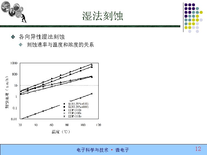
原子层刻蚀Tests Three complementary tests to characterize ALE: 1. Synergy test(协同测试); 2. Saturation curve(饱和曲线) ; Etched amount versus time for a fixed removal energy; 3. Energy scan (能量扫描); Etched amount as a function of energy for a fixed removal time. These tests can help indicate to what degree the ALE process approaches ideal behavior. 电子科学与技术 • 微电子 48
原子层刻蚀Tests ALE will be characterized by the benefits on the wafer: 1. Features with atomically smooth and flat surfaces; 2. Reproducibility of stoichiometry(化学计量); 3. Uniformity across the wafer; 4. Etching without loading (pattern-density independence); 5. Low-damage to remaining material; 6. Etch selectivity to other materials. 电子科学与技术 • 微电子 49
原子层刻蚀Tests The synergy test, Measures the amount of material etched per cycle compared to the amount from each individual step; There is no etching during the modification step ; reaction A. There should be no etching beyond the surface modified layer ; reaction B. Each step may result in removal of some material; But the conditions should be letter changed 电子科学与技术 • 微电子 50
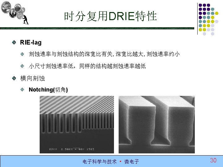
原子层刻蚀Tests The saturation curve test, They are used to determine the degree of self-limiting behavior for the chosen conditions. The Energy scan test Less frequently used ; For the removal step, plotting EPC as a function of energy. 电子科学与技术 • 微电子 51
原子层刻蚀Tests Energy scan test The scan is divided into three regions. 1. The ALE window in Regime II indicates the desirable operating range; 2. Region I represents incomplete etching for low removal energy; 3. Region III represents over-etching for high removal energy (e. g. , sputter). 电子科学与技术 • 微电子 52
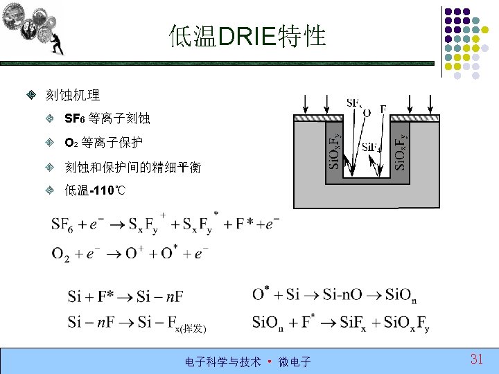
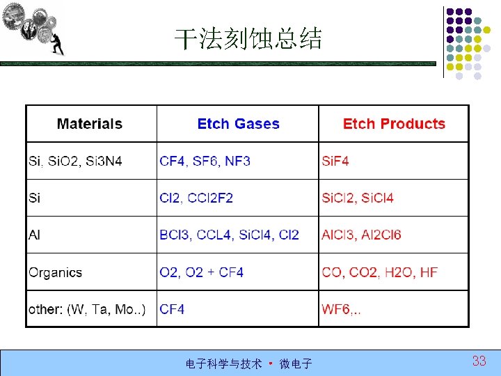
Si原子层刻蚀 采用Cl和Ar完成Si的ALE 艺 A step,Cl与Si形成Si. Clx,x=1, 2, 3, 4; B step,Ar plasma provides ion bombardment to activate removal of the silicon chloride reactive layer。 Cl基 艺还可以刻蚀: 锗; 金属氧化物; III–V 材料. 电子科学与技术 • 微电子 53
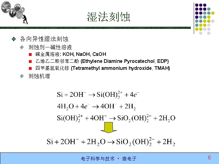
Si原子层刻蚀 Thermal chlorination : Chlorine modifies the silicon surface by chemisorptions; Chlorine gas spontaneously chemisorbs onto a clean silicon surface at room temperature to form a Si. Clx layer: Cl 2 (g) + Si (s) =Si. Clx (s). Each silicon surface atom bonds to one chlorine atom. 电子科学与技术 • 微电子 54
Si原子层刻蚀 Thermal chlorination : The role of chlorine is to weaken the underlying Si–Si bond to make it more easily removable from the pristine silicon lattice; The Si-Cl bonding energy of 4. 2 e. V is stronger than the pristine Si-Si bond of 3. 4 e. V; This lowers the threshold energy for removing the Si. Clx layer with respect to the pristine silicon; The underlying Si-Si bond strength is reduced from 3. 4 e. V down to an estimated 2. 3 e. V. 电子科学与技术 • 微电子 55
Si原子层刻蚀 Thermal chlorination 8– 40 s under typical laboratory conditions. Faster chlorination 1. increasing substrate temperatures ; 2. increasing partial pressure of the chlorine gas. The substrate temperature should be maintained below 650 ℃; 该温度下氯自发刻蚀Si. 电子科学与技术 • 微电子 56
Si原子层刻蚀 Plasma Chlorination Plasma can be used to Speed Up chlorination : Producing highly reactive Chlorine Radicals ; Producing highly Energetic Species。 Chlorinated the silicon surface with pure Cl 2 plasma。 电子科学与技术 • 微电子 57
Si原子层刻蚀 Plasma chlorination The chlorinated silicon surface is more complex with exposure to plasma than from using thermal methods. in processing plasmas, neutral densities typically are several orders of magnitude higher than ion densities; surface chemistry is thought to be dominated by interaction of the silicon wafer with chlorine radicals some influence from chlorine ions, Cl 2+and Cl+, photons, and electrons. 电子科学与技术 • 微电子 58
Si原子层刻蚀 Plasma chlorination (a) Excellent depth uniformity across the wafer; (b) Flat silicon etch front on the feature; (c) Smooth surface. 电子科学与技术 • 微电子 59
Si原子层刻蚀 Argon ion bombardment The removal step is to provide energy to break the Si-Si bonds underneath the surface Si-Cl. This energy can be supplied thermally by raising the wafer temperature to above 650℃for desorption of Si. Cl 2. This results in an isotropic process since both chlorination and thermal desorption are nominally isotropic. High wafer temperatures are detrimental to active devices. Lower processing temperatures are desirable. 电子科学与技术 • 微电子 60
Si原子层刻蚀 Argon ion bombardment Typically 50 e. V Ar+ are directed toward the wafer surface; 84% of the silicon is removed as Si. Cl,EPC is the distance between atomic layers, 0. 14 nm for the Si (100) surface; thermal desorption in silicon ALE involves surface diffusion and the product is expected to be Si. Cl 2 ; The reaction Si - Si. Clx(s) → Si (s) + Si. Cl 2 (g). The first-order estimated EPC would be half a monolayer, or 0. 07 nm. Steric hindrance(位阻现象) and initial surface roughness will also factor into the amount etched per cycle. 电子科学与技术 • 微电子 61
Si 原子层刻蚀 Argon ion bombardment Continuous etching,the removal step can have the effect of resetting the silicon surface after completion of each cycle. Continuous etching accumulate roughness and inhomogeneity. Continuous etching exposes the surface to energetic Ar+, Cl+ , Cl 2+. Energetic reactant ions break Si–Si surface bonds; damage the silicon ; allowing Cl atoms to diffuse and alter the lattice structure. Accumulated surface roughness occurs with the Si-Cl bonding ; high activation barrier for surface diffusion ; prevents flattening of the silicon surface. 电子科学与技术 • 微电子 62
Si原子层刻蚀 Argon ion bombardment ALE, the removal step does not involve reactive chlorine ions ; Chlorine is not intentionally present; Energetic Ar+ can break Si–Si bonds, at Ar+ energy values well below the sputtering threshold; These bonds can reform once the chlorine bonds are removed; This smoothing or resetting effect in silicon ALE is attributed to the higher surface atom mobility under Ar+ bombardment at suitable ion energies. 电子科学与技术 • 微电子 63
Si原子层刻蚀 Plasma sources used for generating the Ar+ in ALE. Electron cyclotron resonance plasma(电子回旋共振等离子源); Helicon source plasma(螺旋形等离子体源); Transformer coupled plasma (TCP) (变换偶合等离子源); Capacitively coupled plasma(电容耦合等离子源); Inductively coupled plasma(电感耦合等离子源). 电子科学与技术 • 微电子 64
Si原子层刻蚀 Other types of energetic species : Ion beams; Neutral beams; Laser beams。 电子科学与技术 • 微电子 65
Si原子层刻蚀 Nonideal reactions Silicon原子层刻蚀 1. Chlorination produces a well-defined reactive layer ; 2. Ar+ remove just this layer。 Nonideal behavior can occur in sub-saturation mode or secondary reactions are present. 1. Etching during chlorination ; 2. Pure sputtering during removal. 电子科学与技术 • 微电子 66
Si 原子层刻蚀用材料 More than 20 materials used in ALE studies; Elemental semiconductors; Compound semiconductors; Insulators; Metals. 电子科学与技术 • 微电子 67
原子层刻蚀 Different modification mechanisms : Chemisorption; Deposition; Conversion (e. g. , oxidation); Plasma assistance; Extraction. Removal methods Thermal desorption; Particle bombardment; Plasma assistance; Chemical reaction 电子科学与技术 • 微电子 69
原子层刻蚀 Different modification mechanisms : 电子科学与技术 • 微电子 70
原子层刻蚀 Silicon ALE Fluorine atoms from CF 4 -plasma at 60℃ in 1990; NF 3; Fluorocarbons; Chlorine has been the reactant of choice in reaction A of silicon ALE most typically by thermal chemisorption; Halogens(卤素) such as Bromine have been studied. 电子科学与技术 • 微电子 71
原子层刻蚀 Oxides ALE Silicon dioxide (Si. O 2) High dielectric constant oxides ; Hafnium oxide (Hf. O 2); Titanium dioxide (Ti. O 2), ; Aluminum oxide (Al 2 O 3); Beryllium oxide (Be. O). Cl 2 was substituted with BCl 3 gas; B-O bonding of 8. 39 e. V is much stronger than Cl- O bonding of 2. 82 e. V, Too weak to form the reactive layer with oxygen in metal oxides。 电子科学与技术 • 微电子 72
原子层刻蚀 Silicon dioxide ALE: 1. Fluorocarbon deposition approach ; 2. Si 3 N 4 approach ; Requires etching narrow (<15 nm) oxide spaces more than 100 nm deep without removing the nitride spacer surrounding the gate; Similar to a Bosch process in that both alternate between deposition and etching steps. 电子科学与技术 • 微电子 73
原子层刻蚀 Silicon dioxide ALE: 3. Silicate salt approach ; The salt is formed when F and N atoms react with Si. O 2 at room temperature to consume the top of the film to form a 5 -10 nm reactive layer; The salt formation is substantially self-limiting; It acts as a diffusion barrier to further reaction at the Si. O 2 interface. 电子科学与技术 • 微电子 74
原子层刻蚀 III–V materials high electron mobility materials ; under consideration as enablers in future devices to replace silicon. Ga. As; Ternary alloy III–Vs Arsenides(砷化物); Phosphides(磷化物); Nitrides(氮化物); Antimonides(锑化物). 电子科学与技术 • 微电子 75
原子层刻蚀 ALE has been studied on several III–V materials: Ga. As; In. P, Al. Ga. As; In. Al. As; Al. Ga. N; The majority are on directional ALE using alternating chlorination and particle bombardment. 电子科学与技术 • 微电子 76
原子层刻蚀 III–V materials Isotropic ALE, Originally referred to as “digital etching” and dating back to the 1990 s; The reactive layer is formed by oxidizing the substrate consuming the topmost surface (reaction A); Oxidized layer thickness 1. 5 nm in Ga. As , 0. 5 nm in Al. Ga. N Followed by removal of the oxidized layer by submerging the wafer into a wet acid bath (e. g. , HCl solution) (reaction B). 电子科学与技术 • 微电子 77
原子层刻蚀 Other materials Copper (Cu) Chlorinating the surface, immersion into dilute HCl bath to dissolve the Cu. Clx product; Chlorinating with plasma, H 2 -plasma to remove the Cu. Clx layer; Germanium (Ge) Chlorination to form the reactive layer, thermal (i. e. , isotropic) removal, or ion-assisted (i. e. , directional) removal; Selectivity to Si or Si. Ge , by controlling temperature of removal: Critical temperature was 260℃ for Ge , 650 ℃ for Si. 电子科学与技术 • 微电子 78
原子层刻蚀 Other materials Graphene Zinc deposited, removed by an acid treatment Caused damage to the top layer of carbon atoms and partially embedded it into the zinc. Oxygen atoms from plasma to form the reactive layer, an Ar neutral beam, removing one monolayer ; Other 2 D structure materials Mo. S 2 电子科学与技术 • 微电子 79
原子层刻蚀 Other materials Polymer Oxygen adsorbed to the surface, low power Ar plasma for removel. Silicon nitride (Si 3 N 4) Used for gate spacers and other parts of devices; Chlorine is not a suitable precursor because Si-N bonding is stronger than Cl-N bonds; Two different ALE approaches for removal of Si 3 N 4. 电子科学与技术 • 微电子 80
原子层刻蚀 Silicon nitride (Si 3 N 4) 1. Directional ALE approach Reaction A , consisted of removing nitrogen on the surface by excited hydrogen gas exposure to form ammonia (NH 3) gas by product; Reaction B, irradiation with low energy ion bombardment. 2. Thin layer etching light ion implantation (H 2 -plasma) ; Implant hydrogen into 10– 20 nm of the surface; Wet etching in aqueous HF solution ; The modified layer an order of magnitude faster than the nonmodified material. 电子科学与技术 • 微电子 81
原子层刻蚀 Other materials Cadmium telluride (Cd. Te) “Extraction” category as the oxidation actually; Extracted specific elements in the compound (e. g. , Cd in Cd. Te) in the top material layer. Au. Sn Extracted in only the topmost layer; Wet etchants removed an atomic layer. Ga. As, Au. Sn, Cd. Te…… 电子科学与技术 • 微电子 82
原子层刻蚀 Conclusion ALE is a technique that removes thin layers of material using sequential selflimiting reactions ; One of the most promising techniques for achieving the low process variability necessary in the atomic-scale era; well-aligned with the needs formation of devices and interconnects below the 10 nm technology node. 电子科学与技术 • 微电子 83