AIDA ASIC review Davide Braga Steve Thomas ASIC
AIDA ASIC review Davide Braga Steve Thomas ASIC Design Group 11 February 2009
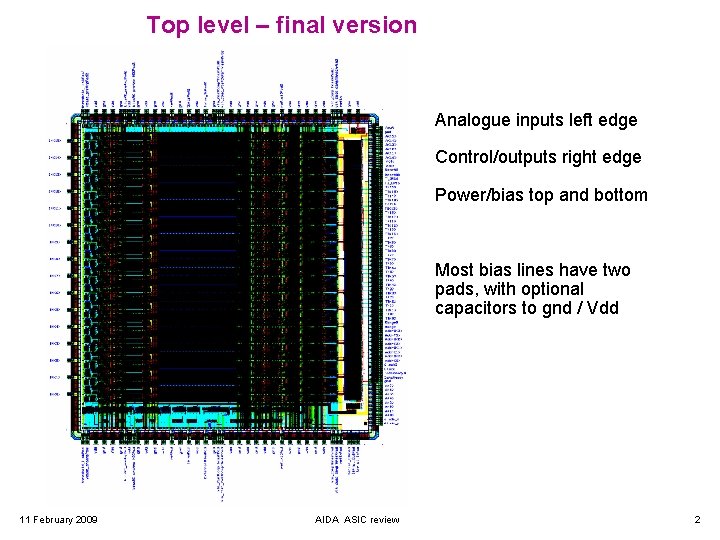
Top level – final version Analogue inputs left edge Control/outputs right edge Power/bias top and bottom Most bias lines have two pads, with optional capacitors to gnd / Vdd 11 February 2009 AIDA ASIC review 2
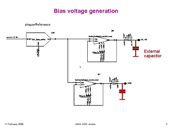
Bias voltage generation External capacitor 11 February 2009 AIDA ASIC review 3

Module wire bonding examples Single-line, parallel bonding Staggered, two-row bonding Tracks with vertical orientation Tracks mostly with vertical orientation Multiple bond wire lengths Power/bias lines horizontally Control signals/outputs vertically 11 February 2009 AIDA ASIC review 4
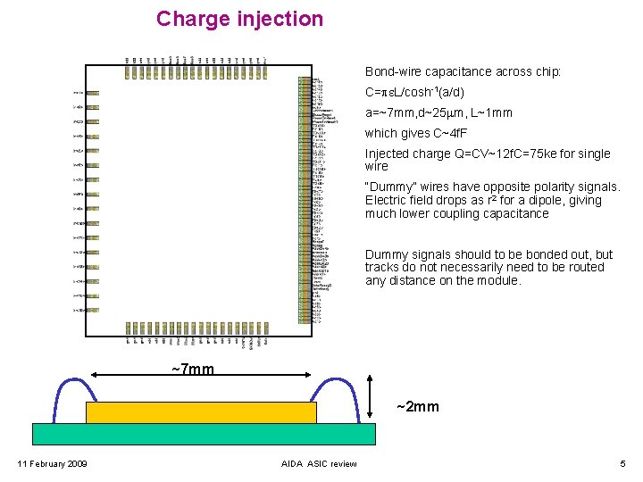
Charge injection Bond-wire parasitics: Bond-wire capacitance across chip: C=pe. L/cosh-1(a/d) a=~7 mm, d~25 mm, L~1 mm which gives C~4 f. F Injected charge Q=CV~12 f. C=75 ke for single wire “Dummy” wires have opposite polarity signals. Electric field drops as r 2 for a dipole, giving much lower coupling capacitance Dummy signals should to be bonded out, but tracks do not necessarily need to be routed any distance on the module. ~7 mm ~2 mm 11 February 2009 AIDA ASIC review 5
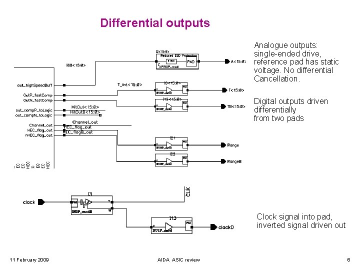
Differential outputs Analogue outputs: single-ended drive, reference pad has static voltage. No differential Cancellation. Digital outputs driven differentially from two pads Clock signal into pad, inverted signal driven out 11 February 2009 AIDA ASIC review 6
Future work: • • Updates of documentation (pad definitions, functions, waveforms). Preparation for testing – adapter board, waveform definitions, IMS chip tester interfacing. Test report, including defining the optimal waveforms and analogue bias point. Module floor-planning, capacitor selection, track resistance analysis. Time-scales: • • • Delivery of 100 ASICs : 20 th April Bonding into 40 -pin dual-in-line packages: 1 week Bonding onto modules: 1 week Preliminary testing: 2 weeks Waveform optimisation: 2 weeks Bias optimisation: 2 weeks 11 February 2009 AIDA ASIC review 7
- Slides: 7