Agilent Technologies Inc EEsof User Group Meeting 2010
- Slides: 43

Agilent Technologies Inc EEsof User Group Meeting 2010 India Phase Locked Loop Nat. Tel Microsystems Pvt. Ltd. Anurag Bhargava Anurag Nigam Application Consultant EEsof EDA Agilent Technologies (India) Private Limited Senior Engineer Nat. Tel Microsystems Private Limited Contact HP: +919845611163 anurag_bhargava@agilent. com www. agilent. com Contact HP: +919765844016 anurag_nigam@nattelmicro. com www. nattelmicro. com

EEsof 2010 User Group Meeting Abstract For very first time, Fractional-N Phase Locked Loop (PLL) Circuit in CMOS Technology is created and simulated in ADS. Unique features of Fractional-N PLL are- • Fully Programmable Dual Band PLL for Wi. Fi & Wi. MAX Bands (2. 3 -2. 7 GHz & 3. 3 -3. 7 GHz) • Fully Differential Loop to minimize digital & substrate noise pickup • Very High Output Impedance Charge Pump for low leakage • Matched Source & Sink Currents • Oscillator based feedback dithering to minimize fractional spurs • Wide range of choice for Crystal (Large Divide Ratio Range 32 -127) • 130 m. W Power Consumption from 3 V DC supply Nat. Tel Microsystems Pvt. Ltd. Engraving the beginning of a New Era in Technologies

EEsof 2010 User Group Meeting Contents of Presentation is divided into following sections a) PLL Applications b) PLL Functionalities c) PLL Overview d) Operation Principle- Fixed-N Vs Fractional-N e) Fractional-N PLL Block Diagram f) PLL Sub-Circuits & Performance g) PLL Integration h) PLL Locking i) Future Scope for Work Nat. Tel Microsystems Pvt. Ltd. Engraving the beginning of a New Era in Technologies

EEsof 2010 User Group Meeting PLL Sub-Circuits List of PLL Sub-circuits 1. 2. 3. 4. 5. 6. 7. 8. 9. 10. 11. 12. 13. 14. 15. 16. 17. 18. 19. 20. 21. 22. High Speed Full Adder Half Adder Multi-bit Adder CML D Latches AND Gated CML D Latches High Impedance Regulated Current Mirrors Charge Pump PPCL NAND Gate PPCL NOT Gate Transmission Gate XOR NOT Gate CML Buffer Level Shifter Level Splitter CML MUX CML to CMOS Converters CMOS to CML Converters Transmission Gate Master Slave D Latch with Reset 2/3 Pre-scalar 5/6 bit Pre-scalar OP Amp 23. 24. 25. 26. 27. 28. 29. 30. Differential Zero-Dead Zone PDF Up Conversion Mixers Divide by Two Accumulator Differencing Compensation Circuit MASH 1 -1 -1 Sigma Delta Modulator Voltage Controlled Oscillators Third Order Loop Filters All the sub-circuits will not be discussed at transistor level in this presentation. Operation and Simulation of these sub-circuits will be demonstrated. Nat. Tel Microsystems Pvt. Ltd. Engraving the beginning of a New Era in Technologies

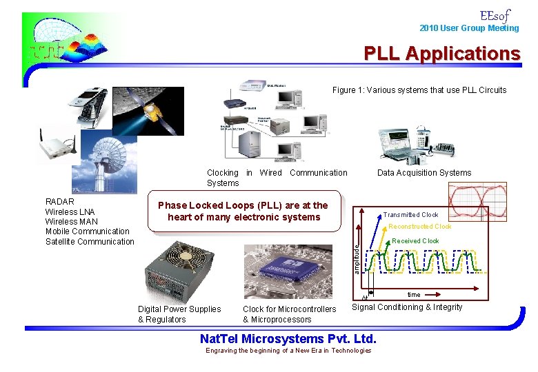
EEsof 2010 User Group Meeting PLL Applications Figure 1: Various systems that use PLL Circuits Clocking in Wired Communication Systems Phase Locked Loops (PLL) are at the heart of many electronic systems Transmitted Clock Reconstructed Clock Received Clock amplitude RADAR Wireless LNA Wireless MAN Mobile Communication Satellite Communication Data Acquisition Systems Δt Digital Power Supplies & Regulators Clock for Microcontrollers & Microprocessors time Signal Conditioning & Integrity Nat. Tel Microsystems Pvt. Ltd. Engraving the beginning of a New Era in Technologies

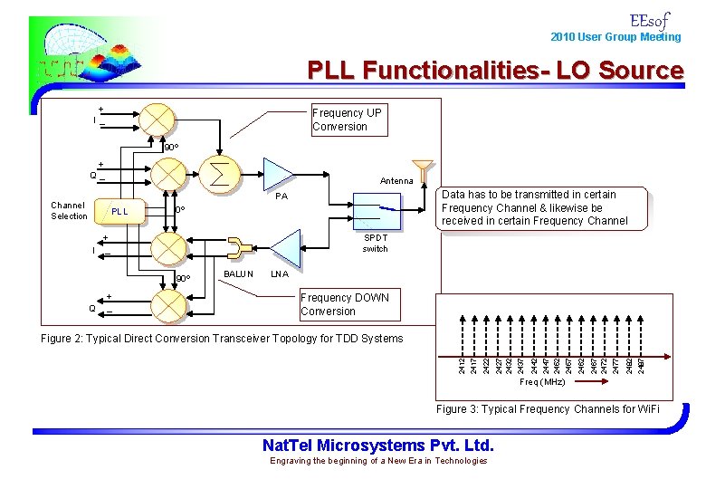
EEsof 2010 User Group Meeting PLL Functionalities- LO Source + I _ Frequency UP Conversion 90º + Q_ Antenna Data has to be transmitted in certain Frequency Channel & likewise be received in certain Frequency Channel PA Channel Selection PLL 0º + I _ SPDT switch 90º Q + _ BALUN LNA Frequency DOWN Conversion 2487 2482 2477 2462 2467 2472 2457 2442 2447 2452 2437 2422 2427 2432 2417 Figure 2: Typical Direct Conversion Transceiver Topology for TDD Systems Freq (MHz) Figure 3: Typical Frequency Channels for Wi. Fi Nat. Tel Microsystems Pvt. Ltd. Engraving the beginning of a New Era in Technologies

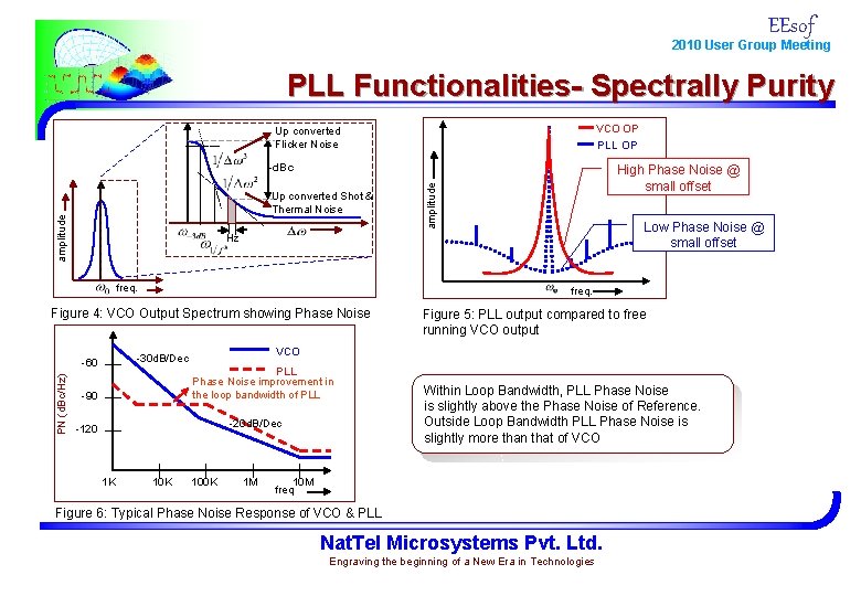
EEsof 2010 User Group Meeting PLL Functionalities- Spectrally Purity VCO OP Up converted Flicker Noise PLL OP -d. Bc Low Phase Noise @ small offset Hz freq. Figure 4: VCO Output Spectrum showing Phase Noise PLL Phase Noise improvement in the loop bandwidth of PLL -90 -20 d. B/Dec -120 1 K 10 K Figure 5: PLL output compared to free running VCO output VCO -30 d. B/Dec -60 PN (d. Bc/Hz) amplitude Up converted Shot & Thermal Noise High Phase Noise @ small offset 100 K 1 M Within Loop Bandwidth, PLL Phase Noise is slightly above the Phase Noise of Reference. Outside Loop Bandwidth PLL Phase Noise is slightly more than that of VCO 10 M freq Figure 6: Typical Phase Noise Response of VCO & PLL Nat. Tel Microsystems Pvt. Ltd. Engraving the beginning of a New Era in Technologies

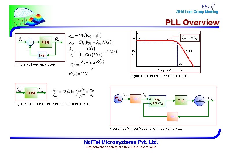
EEsof 2010 User Group Meeting PLL Overview N G(s) CL(s) _ + H(s) G(s) Figure 7 : Feedback Loop Freq (or s) Figure 8: Frequency Response of PLL CL(s) 1/R Figure 9 : Closed Loop Transfer Function of PLL PFD CP ( ) Z (s) 1/N Figure 10 : Analog Model of Charge Pump PLL Nat. Tel Microsystems Pvt. Ltd. Engraving the beginning of a New Era in Technologies

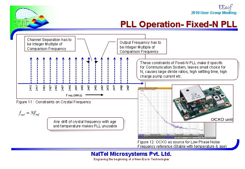
EEsof 2010 User Group Meeting PLL Operation- Fixed-N PLL Channel Separation has to be Integer Multiple of Comparison Frequency Output Frequency has to be Integer Multiple of Comparison Frequency 2487 2482 2477 2472 2467 2462 2457 2452 2447 2442 2437 2432 2427 2422 2417 2412 These constraints of Fixed-N PLL make it specific for Communication System, leaves small choice for N, causes large divide ratios, high settling time, high charge pump current etc. Freq (MHz) Figure 11 : Constraints on Crystal Frequency Any drift of crystal frequency with age and temperature makes PLL unusable Figure 12: OCXO as source for Low Phase Noise Frequency reference (Stable with temperature & age) Nat. Tel Microsystems Pvt. Ltd. Engraving the beginning of a New Era in Technologies

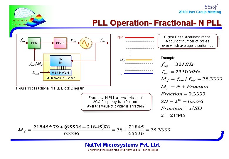
EEsof 2010 User Group Meeting PLL Operation- Fractional- N PLL N+1 PFD CP/LF Example % Mf 6 -bit D Word Sigma Delta Modulator keeps account of number of cycles over which average is performed N Multi-modulus Divider Figure 13 : Fractional N PLL Block Diagram Fractional N PLL allows division of VCO frequency by a fraction. Average value of divider is a fraction Nat. Tel Microsystems Pvt. Ltd. Engraving the beginning of a New Era in Technologies

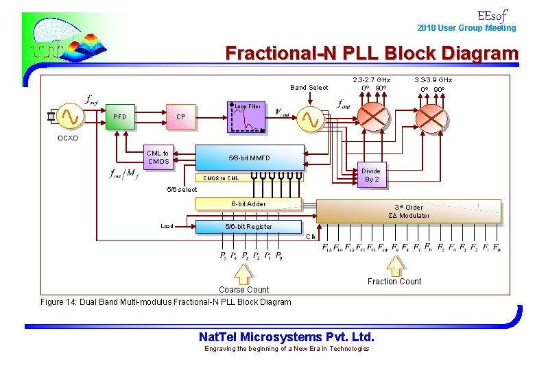
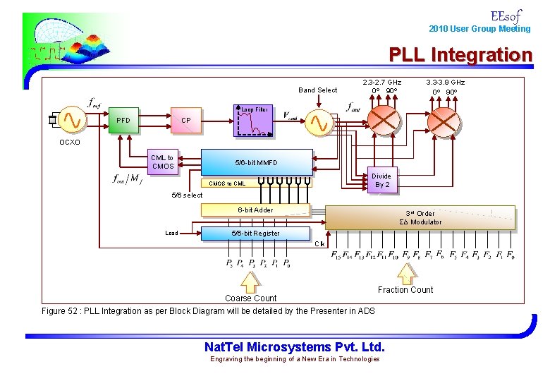
EEsof 2010 User Group Meeting Fractional-N PLL Block Diagram Band Select 2. 3 -2. 7 GHz 0º 90º 3. 3 -3. 9 GHz 0º 90º Loop Filter PFD CP OCXO CML to CMOS 5/6 -bit MMFD Divide By 2 CMOS to CML 5/6 select 6 -bit Adder Load 3 rd Order ƩΔ Modulator 5/6 -bit Register Clk Coarse Count Figure 14: Dual Band Multi-modulus Fractional-N PLL Block Diagram Fraction Count Nat. Tel Microsystems Pvt. Ltd. Engraving the beginning of a New Era in Technologies

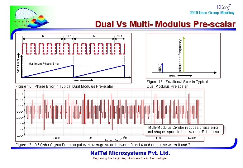
EEsof 2010 User Group Meeting Dual Vs Multi- Modulus Pre-scalar N Maximum Phase Error N+1 reference frequency N+1 spur Phase Error N freq. time Figure 15 : Phase Error in Typical Dual Modulus Pre-scalar Figure 16 : Fractional Spur in Typical Dual Modulus Pre-scalar Multi-Modulus Divider reduces phase error and shapes spurs to be low near PLL output Figure 17 : 3 rd Order Sigma Delta output with average value between 3 and 4 and output between 0 and 7 Nat. Tel Microsystems Pvt. Ltd. Engraving the beginning of a New Era in Technologies

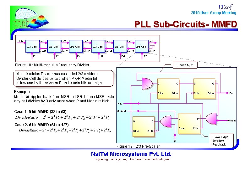
EEsof 2010 User Group Meeting PLL Sub-Circuits- MMFD Fo 1 Fin 2/3 Cell Fo 2 2/3 Cell Mod 1 P 0 Fo 4 2/3 Cell Mod 2 P 1 Fo 5 2/3 Cell Mod 3 P 2 Fo 5 Fo 6 2/3 Cell Mod 4 P 3 2/3 Cell Mod 5 P 4 Mod 6 P 5 Figure 18 : Multi-modulus Frequency Divider Divide by 2 Multi-Modulus Divider has cascaded 2/3 dividers Divider Cell divides by two when P OR Modin bit is low and by three when P and Modin bits are high Example Modin bit ripples back from MSB to LSB. In one MSB cycle any cell divides by 3 only once when P and Modin is high. Case 1 - 5 bit MMFD (32 to 63) Case 2 - 6 bit MMFD (64 to 127) D CLK D Q Qbar Q CLK Fo Qbar Fin Modout Q Qbar Q D Qbar CLK P Figure 19 : 2/3 Pre-Scalar Nat. Tel Microsystems Pvt. Ltd. Engraving the beginning of a New Era in Technologies D Modin CLK Clock Edge Swallow Feedback

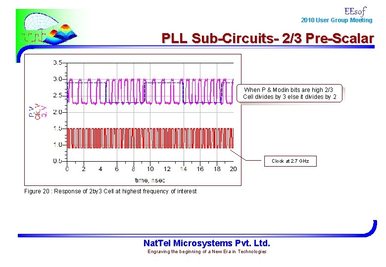
EEsof 2010 User Group Meeting PLL Sub-Circuits- 2/3 Pre-Scalar When P & Modin bits are high 2/3 Cell divides by 3 else it divides by 2 Clock at 2. 7 GHz Figure 20 : Response of 2 by 3 Cell at highest frequency of interest Nat. Tel Microsystems Pvt. Ltd. Engraving the beginning of a New Era in Technologies

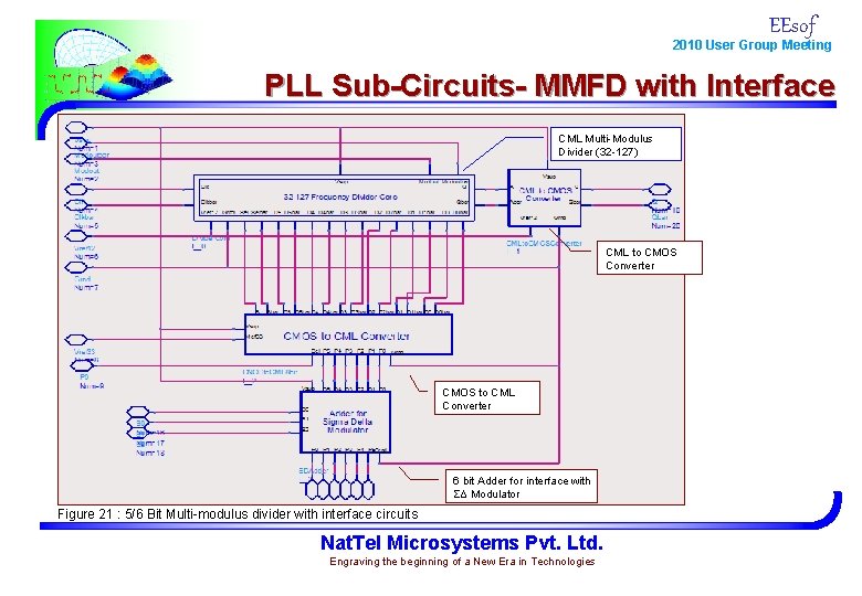
EEsof 2010 User Group Meeting PLL Sub-Circuits- MMFD with Interface CML Multi-Modulus Divider (32 -127) CML to CMOS Converter CMOS to CML Converter 6 bit Adder for interface with ƩΔ Modulator Figure 21 : 5/6 Bit Multi-modulus divider with interface circuits Nat. Tel Microsystems Pvt. Ltd. Engraving the beginning of a New Era in Technologies

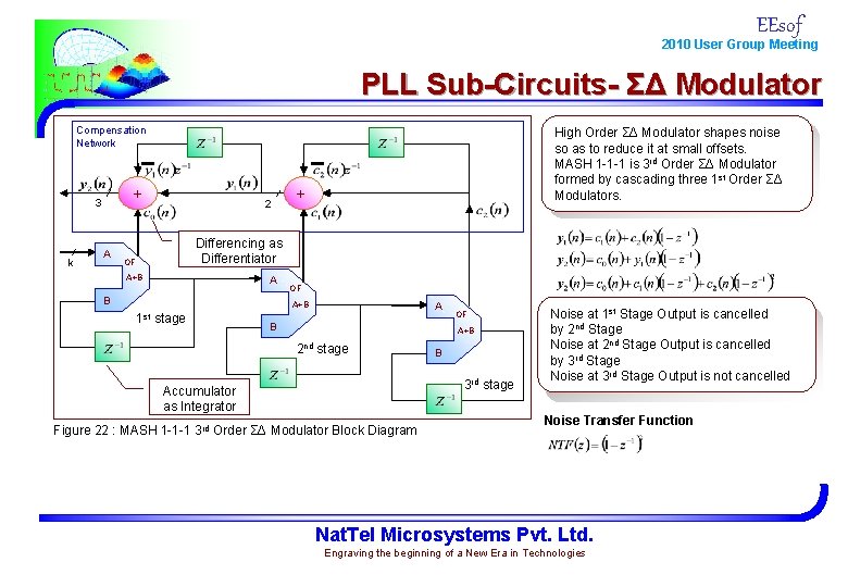
EEsof 2010 User Group Meeting PLL Sub-Circuits- ƩΔ Modulator Compensation Network + 3 k A 2 High Order ƩΔ Modulator shapes noise so as to reduce it at small offsets. MASH 1 -1 -1 is 3 rd Order ƩΔ Modulator formed by cascading three 1 st Order ƩΔ Modulators. + Differencing as Differentiator OF A+B A B OF A+B 1 st stage A B OF A+B 2 nd stage B 3 rd stage Accumulator as Integrator Figure 22 : MASH 1 -1 -1 3 rd Order ƩΔ Modulator Block Diagram Noise at 1 st Stage Output is cancelled by 2 nd Stage Noise at 2 nd Stage Output is cancelled by 3 rd Stage Noise at 3 rd Stage Output is not cancelled Noise Transfer Function Nat. Tel Microsystems Pvt. Ltd. Engraving the beginning of a New Era in Technologies

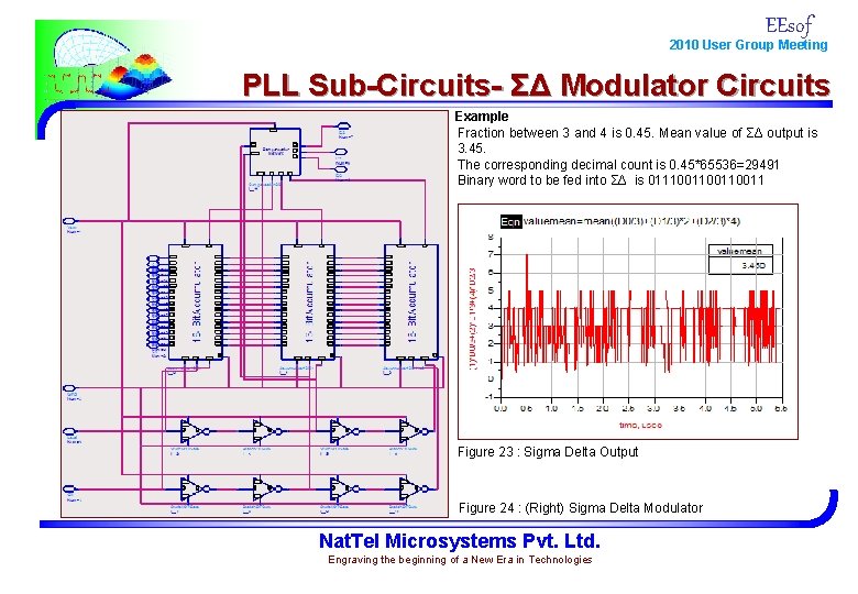
EEsof 2010 User Group Meeting PLL Sub-Circuits- ƩΔ Modulator Circuits Example Fraction between 3 and 4 is 0. 45. Mean value of ƩΔ output is 3. 45. The corresponding decimal count is 0. 45*65536=29491 Binary word to be fed into ƩΔ is 011100110011 Figure 23 : Sigma Delta Output Figure 24 : (Right) Sigma Delta Modulator Nat. Tel Microsystems Pvt. Ltd. Engraving the beginning of a New Era in Technologies

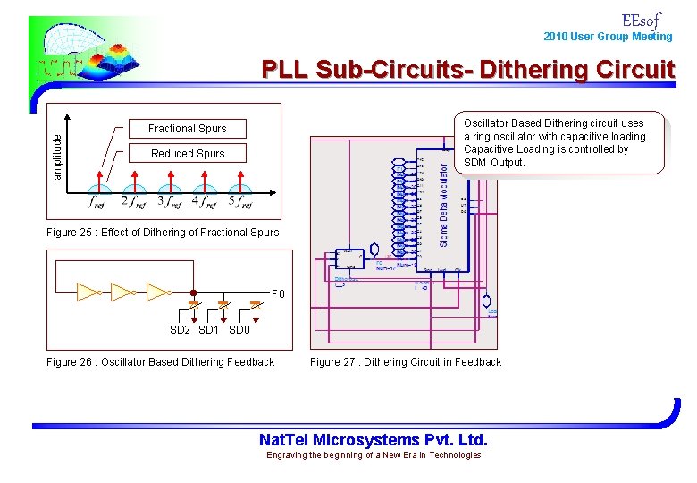
EEsof 2010 User Group Meeting amplitude PLL Sub-Circuits- Dithering Circuit Oscillator Based Dithering circuit uses a ring oscillator with capacitive loading. Capacitive Loading is controlled by SDM Output. Fractional Spurs Reduced Spurs Figure 25 : Effect of Dithering of Fractional Spurs F 0 SD 2 SD 1 SD 0 Figure 26 : Oscillator Based Dithering Feedback Figure 27 : Dithering Circuit in Feedback Nat. Tel Microsystems Pvt. Ltd. Engraving the beginning of a New Era in Technologies

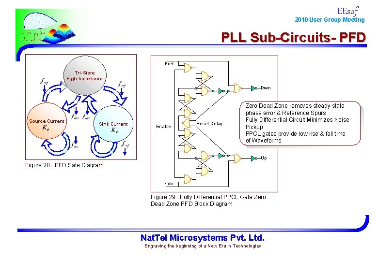
EEsof 2010 User Group Meeting PLL Sub-Circuits- PFD Fref Tri-State High Impedance Dwn Source Current Sink Current Enable Reset Delay Zero Dead Zone removes steady state phase error & Reference Spurs Fully Differential Circuit Minimizes Noise Pickup PPCL gates provide low rise & fall time of Waveforms Up Figure 28 : PFD Sate Diagram Fdiv Figure 29 : Fully Differential PPCL Gate Zero Dead Zone PFD Block Diagram Nat. Tel Microsystems Pvt. Ltd. Engraving the beginning of a New Era in Technologies

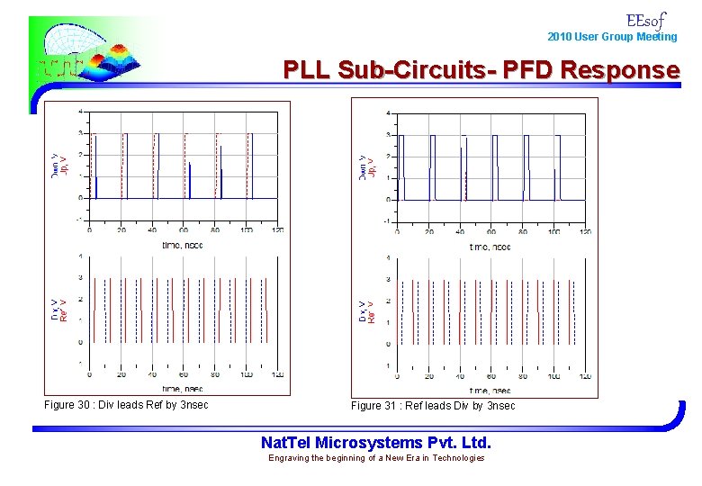
EEsof 2010 User Group Meeting PLL Sub-Circuits- PFD Response Figure 30 : Div leads Ref by 3 nsec Figure 31 : Ref leads Div by 3 nsec Nat. Tel Microsystems Pvt. Ltd. Engraving the beginning of a New Era in Technologies

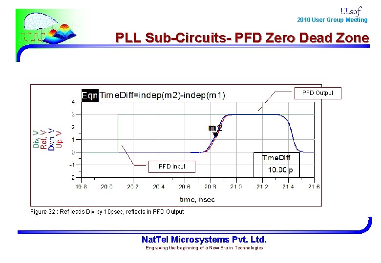
EEsof 2010 User Group Meeting PLL Sub-Circuits- PFD Zero Dead Zone PFD Output PFD Input Figure 32 : Ref leads Div by 10 psec, reflects in PFD Output Nat. Tel Microsystems Pvt. Ltd. Engraving the beginning of a New Era in Technologies

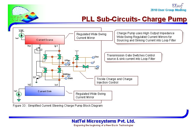
EEsof 2010 User Group Meeting PLL Sub-Circuits- Charge Pump Vdd Iref Regulated Wide Swing Current Mirror Current Source Inp Charge Pump uses High Output Impedance Wide Swing Regulated Current Mirrors for Sourcing and Sinking Current into Loop Filter Ip 1 Q 2 Cbar UPbar Transmission Gate Switches Control source & sink current into Loop Filter C UP To. LF DWNbar Q 1 DWN In 2 Iref In 1 Current Sink Trickle Charge and Charge Injection Control Regulated Wide Swing Current Mirror Figure 33 : Simplified Current Steering Charge Pump Block Diagram Nat. Tel Microsystems Pvt. Ltd. Engraving the beginning of a New Era in Technologies

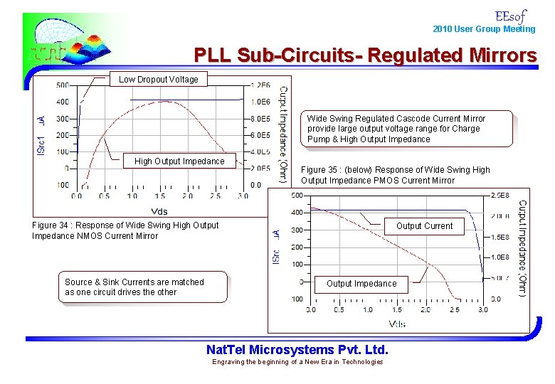
EEsof 2010 User Group Meeting PLL Sub-Circuits- Regulated Mirrors Low Dropout Voltage Wide Swing Regulated Cascode Current Mirror provide large output voltage range for Charge Pump & High Output Impedance Figure 35 : (below) Response of Wide Swing High Output Impedance PMOS Current Mirror Figure 34 : Response of Wide Swing High Output Impedance NMOS Current Mirror Source & Sink Currents are matched as one circuit drives the other Output Current Output Impedance Nat. Tel Microsystems Pvt. Ltd. Engraving the beginning of a New Era in Technologies

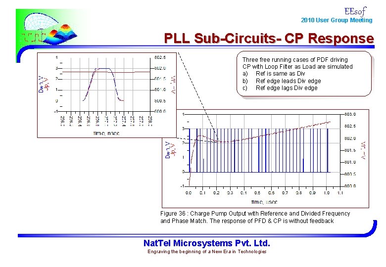
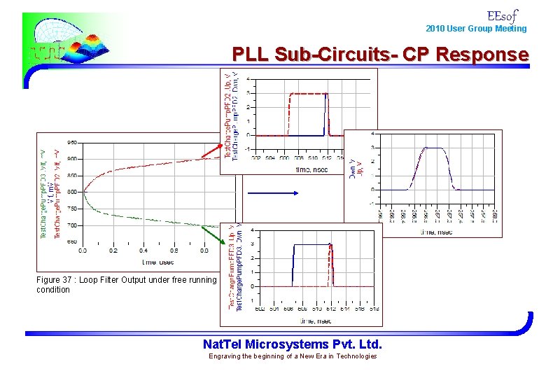
EEsof 2010 User Group Meeting PLL Sub-Circuits- CP Response Three free running cases of PDF driving CP with Loop Filter as Load are simulated a) Ref is same as Div b) Ref edge leads Div edge c) Ref edge lags Div edge Figure 36 : Charge Pump Output with Reference and Divided Frequency and Phase Match. The response of PFD & CP is without feedback Nat. Tel Microsystems Pvt. Ltd. Engraving the beginning of a New Era in Technologies

EEsof 2010 User Group Meeting PLL Sub-Circuits- CP Response Figure 37 : Loop Filter Output under free running condition Nat. Tel Microsystems Pvt. Ltd. Engraving the beginning of a New Era in Technologies

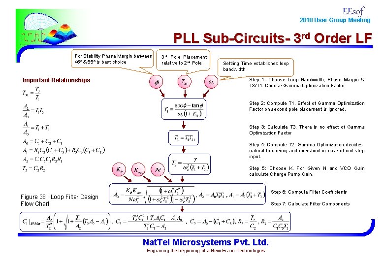
EEsof 2010 User Group Meeting PLL Sub-Circuits- 3 rd Order LF For Stability Phase Margin between 45º & 55º is best choice Important Relationships 3 rd Pole Placement relative to 2 nd Pole Settling Time establishes loop bandwidth Step 1: Choose Loop Bandwidth, Phase Margin & T 3/T 1. Choose Gamma Optimization Factor Step 2: Compute T 1. Effect of Gamma Optimization Factor on second pole placement is ignored. Step 3: Calculate T 3. There is no effect of Gamma Optimization Factor Step 4: Compute T 2. Gamma Optimization decides natural frequency and overshoot in case of unit step input. Step 5: Choose K. For Given N and VCO Gain calculate Charge Pump Gain. Step 6: Compute Filter Coefficients Figure 38 : Loop Filter Design Flow Chart Step 7: Calculate Filter Components Nat. Tel Microsystems Pvt. Ltd. Engraving the beginning of a New Era in Technologies

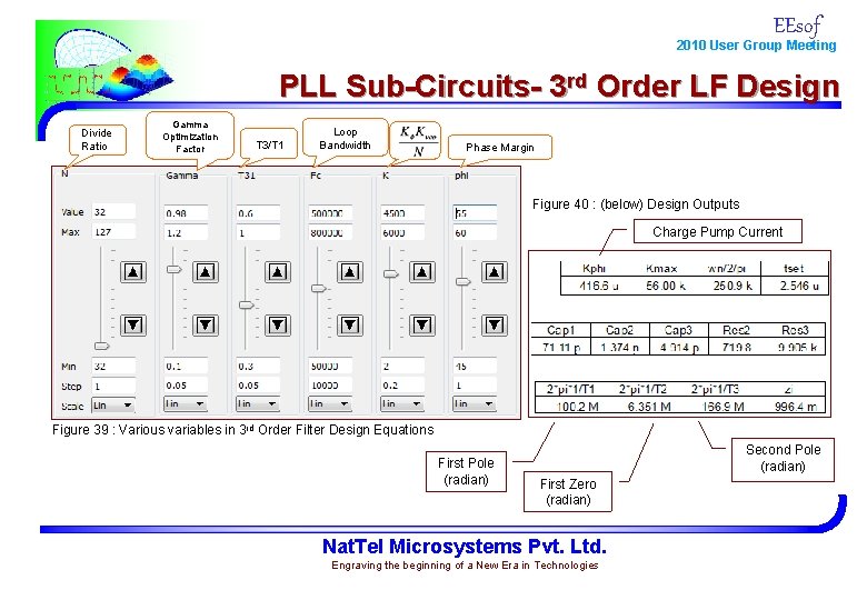
EEsof 2010 User Group Meeting PLL Sub-Circuits- 3 rd Order LF Design Divide Ratio Gamma Optimization Factor T 3/T 1 Loop Bandwidth Phase Margin Figure 40 : (below) Design Outputs Charge Pump Current Figure 39 : Various variables in 3 rd Order Filter Design Equations First Pole (radian) Second Pole (radian) First Zero (radian) Nat. Tel Microsystems Pvt. Ltd. Engraving the beginning of a New Era in Technologies

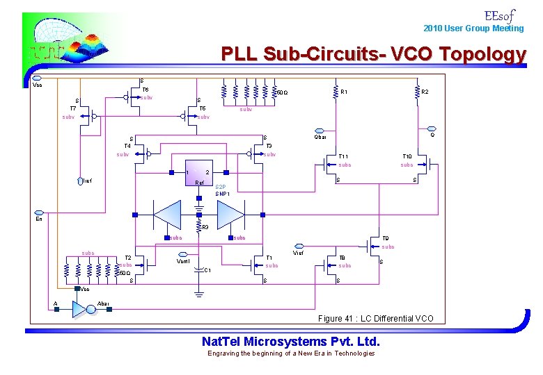
EEsof 2010 User Group Meeting PLL Sub-Circuits- VCO Topology S Vcc T 6 subv S T 7 subv R 2 R 1 50Ω S T 5 subv T 3 subv 1 Iref Q Qbar S S T 4 subv T 11 subc T 10 subc 2 S Ref S S 2 P SNP 1 En R 3 subc T 2 subc 50Ω S subc Vcntl C 1 T 9 subc T 1 subc S Vref T 8 subc S S Vcc A Abar Figure 41 : LC Differential VCO Nat. Tel Microsystems Pvt. Ltd. Engraving the beginning of a New Era in Technologies

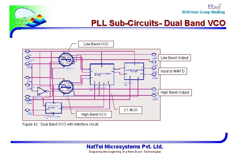
EEsof 2010 User Group Meeting PLL Sub-Circuits- Dual Band VCO Low Band Output Input to MMFD High Band Output 2: 1 MUX High Band VCO Figure 42 : Dual Band VCO with interface circuit Nat. Tel Microsystems Pvt. Ltd. Engraving the beginning of a New Era in Technologies

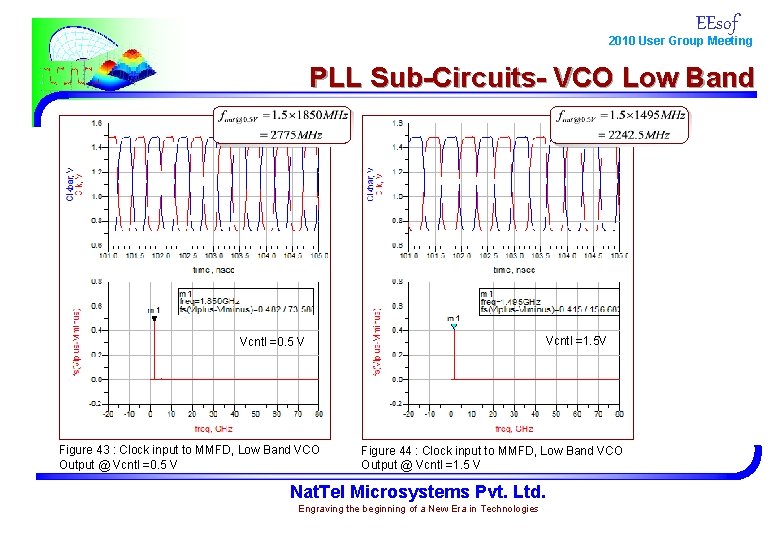
EEsof 2010 User Group Meeting PLL Sub-Circuits- VCO Low Band Vcntl =1. 5 V Vcntl =0. 5 V Figure 43 : Clock input to MMFD, Low Band VCO Output @ Vcntl =0. 5 V Figure 44 : Clock input to MMFD, Low Band VCO Output @ Vcntl =1. 5 V Nat. Tel Microsystems Pvt. Ltd. Engraving the beginning of a New Era in Technologies

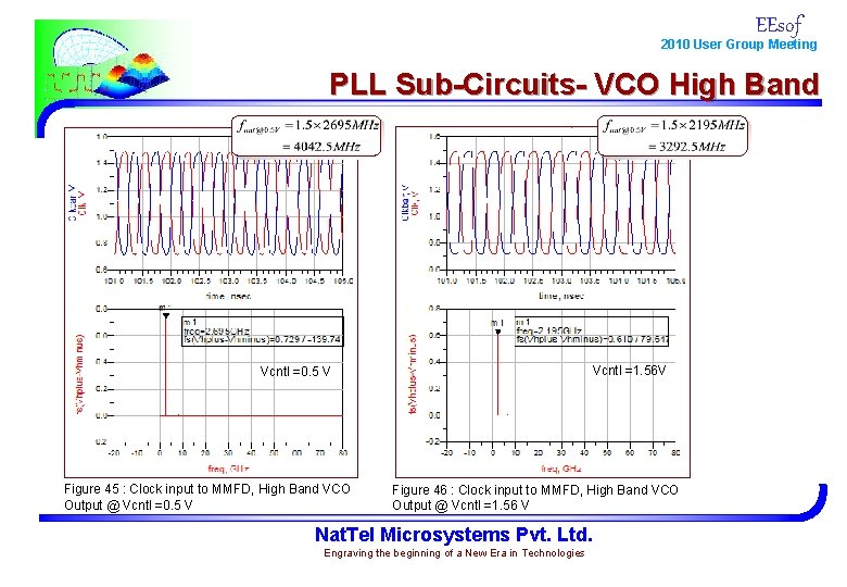
EEsof 2010 User Group Meeting PLL Sub-Circuits- VCO High Band Vcntl =1. 56 V Vcntl =0. 5 V Figure 45 : Clock input to MMFD, High Band VCO Output @ Vcntl =0. 5 V Figure 46 : Clock input to MMFD, High Band VCO Output @ Vcntl =1. 56 V Nat. Tel Microsystems Pvt. Ltd. Engraving the beginning of a New Era in Technologies

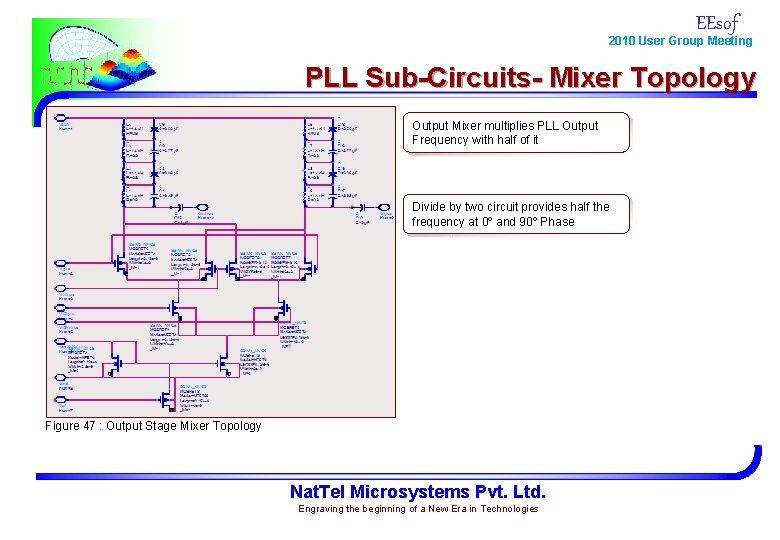
EEsof 2010 User Group Meeting PLL Sub-Circuits- Mixer Topology Output Mixer multiplies PLL Output Frequency with half of it Divide by two circuit provides half the frequency at 0º and 90º Phase Figure 47 : Output Stage Mixer Topology Nat. Tel Microsystems Pvt. Ltd. Engraving the beginning of a New Era in Technologies

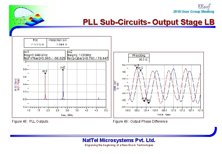
EEsof 2010 User Group Meeting PLL Sub-Circuits- Output Stage LB Figure 48 : PLL Outputs Figure 49 : Output Phase Difference Nat. Tel Microsystems Pvt. Ltd. Engraving the beginning of a New Era in Technologies

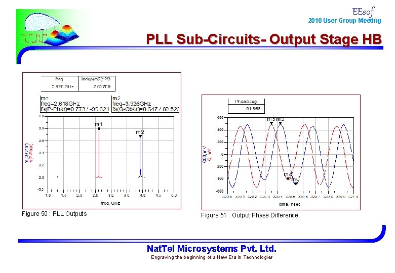
EEsof 2010 User Group Meeting PLL Sub-Circuits- Output Stage HB Figure 50 : PLL Outputs Figure 51 : Output Phase Difference Nat. Tel Microsystems Pvt. Ltd. Engraving the beginning of a New Era in Technologies

EEsof 2010 User Group Meeting PLL Integration Band Select 2. 3 -2. 7 GHz 0º 90º 3. 3 -3. 9 GHz 0º 90º Loop Filter PFD CP OCXO CML to CMOS 5/6 -bit MMFD Divide By 2 CMOS to CML 5/6 select 6 -bit Adder Load 3 rd Order ƩΔ Modulator 5/6 -bit Register Clk Coarse Count Figure 52 : PLL Integration as per Block Diagram will be detailed by the Presenter in ADS Fraction Count Nat. Tel Microsystems Pvt. Ltd. Engraving the beginning of a New Era in Technologies

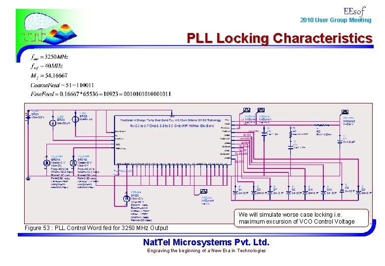
EEsof 2010 User Group Meeting PLL Locking Characteristics Figure 53 : PLL Control Word fed for 3250 MHz Output We will simulate worse case locking i. e. maximum excursion of VCO Control Voltage Nat. Tel Microsystems Pvt. Ltd. Engraving the beginning of a New Era in Technologies

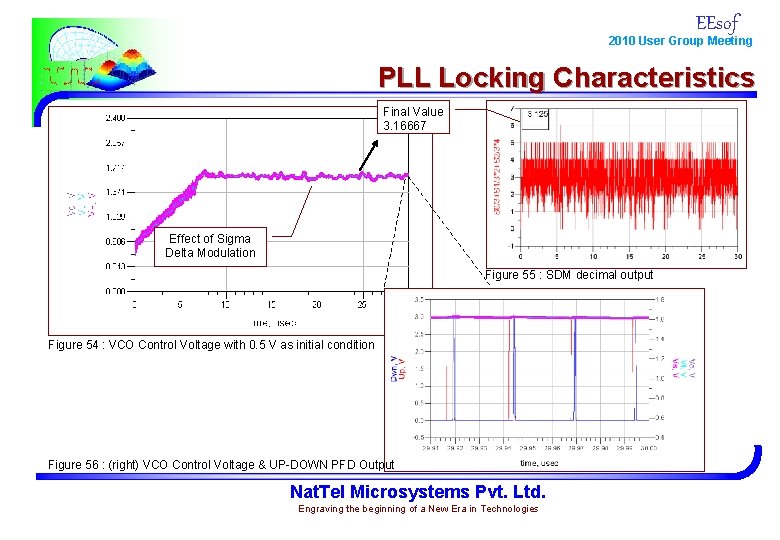
EEsof 2010 User Group Meeting PLL Locking Characteristics Final Value 3. 16667 Effect of Sigma Delta Modulation Figure 55 : SDM decimal output Figure 54 : VCO Control Voltage with 0. 5 V as initial condition Figure 56 : (right) VCO Control Voltage & UP-DOWN PFD Output Nat. Tel Microsystems Pvt. Ltd. Engraving the beginning of a New Era in Technologies

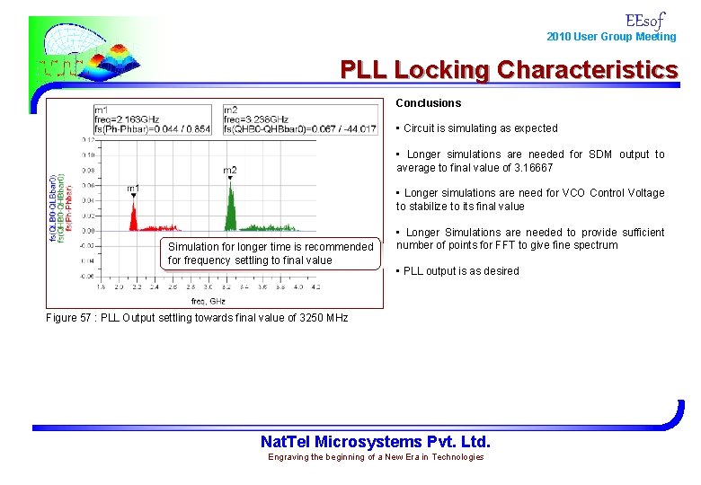
EEsof 2010 User Group Meeting PLL Locking Characteristics Conclusions • Circuit is simulating as expected • Longer simulations are needed for SDM output to average to final value of 3. 16667 • Longer simulations are need for VCO Control Voltage to stabilize to its final value Simulation for longer time is recommended for frequency settling to final value • Longer Simulations are needed to provide sufficient number of points for FFT to give fine spectrum • PLL output is as desired Figure 57 : PLL Output settling towards final value of 3250 MHz Nat. Tel Microsystems Pvt. Ltd. Engraving the beginning of a New Era in Technologies

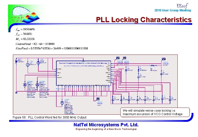
EEsof 2010 User Group Meeting PLL Locking Characteristics Figure 58 : PLL Control Word fed for 3850 MHz Output We will simulate worse case locking i. e. maximum excursion of VCO Control Voltage Nat. Tel Microsystems Pvt. Ltd. Engraving the beginning of a New Era in Technologies

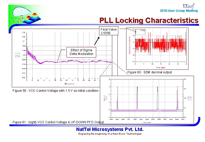
EEsof 2010 User Group Meeting PLL Locking Characteristics Final Value 3. 5556 Effect of Sigma Delta Modulation Figure 60 : SDM decimal output Figure 59 : VCO Control Voltage with 1. 5 V as initial condition Figure 61 : (right) VCO Control Voltage & UP-DOWN PFD Output Nat. Tel Microsystems Pvt. Ltd. Engraving the beginning of a New Era in Technologies

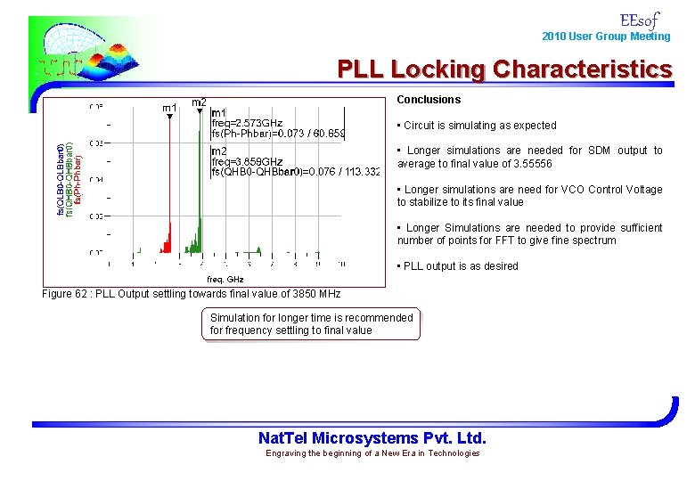
EEsof 2010 User Group Meeting PLL Locking Characteristics Conclusions • Circuit is simulating as expected • Longer simulations are needed for SDM output to average to final value of 3. 55556 • Longer simulations are need for VCO Control Voltage to stabilize to its final value • Longer Simulations are needed to provide sufficient number of points for FFT to give fine spectrum • PLL output is as desired Figure 62 : PLL Output settling towards final value of 3850 MHz Simulation for longer time is recommended for frequency settling to final value Nat. Tel Microsystems Pvt. Ltd. Engraving the beginning of a New Era in Technologies

EEsof 2010 User Group Meeting Future Scope Current Effort is still in progress. The circuit is created and layout is performed in Cadence. Various activities in progress are • Phase Noise Simulations are performed using Envelope Simulations with time duration of few milliseconds • Dither Oscillator Frequency and load are fine tuned for best fractional spur performance • Dual Edge Triggered SDM is expected to further reduce reference spurs • Source & Sink Currents are fine tuned based on leakage • Efficient Layout is underway in 0. 13 um Silterra CMOS Process Nat. Tel Microsystems Pvt. Ltd. Engraving the beginning of a New Era in Technologies

Agilent Technologies Inc EEsof User Group Meeting 2010 India Thank You Nat. Tel Microsystems Pvt. Ltd. Anurag Nigam