Advanced Semiconductor Fundamentals Chapter 5 RecombinationGeneration Processes Chapter
Advanced Semiconductor Fundamentals Chapter 5. Recombination-Generation Processes Chapter 5 Recombination-Generation Process Jung-Hee Lee @ Nitride Semiconductor Device Lab.
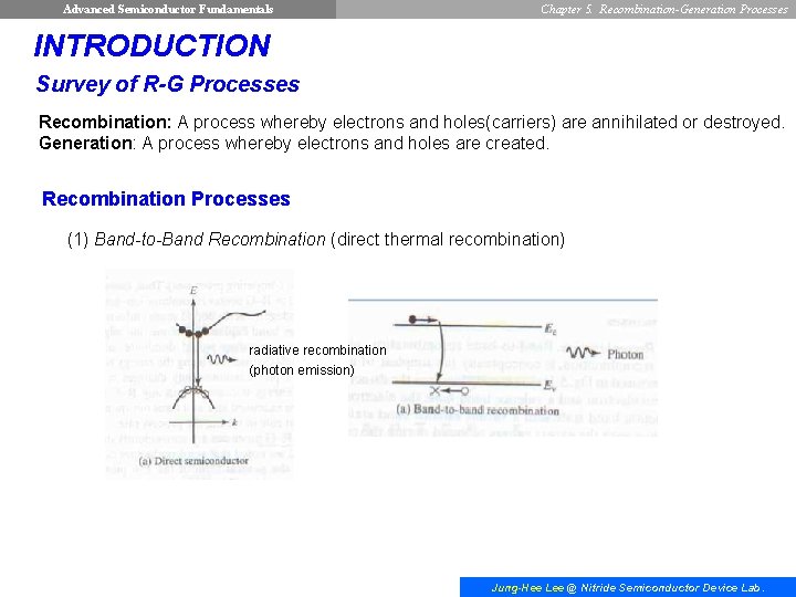
Advanced Semiconductor Fundamentals Chapter 5. Recombination-Generation Processes INTRODUCTION Survey of R-G Processes Recombination: A process whereby electrons and holes(carriers) are annihilated or destroyed. Generation: A process whereby electrons and holes are created. Recombination Processes (1) Band-to-Band Recombination (direct thermal recombination) radiative recombination (photon emission) Jung-Hee Lee @ Nitride Semiconductor Device Lab.
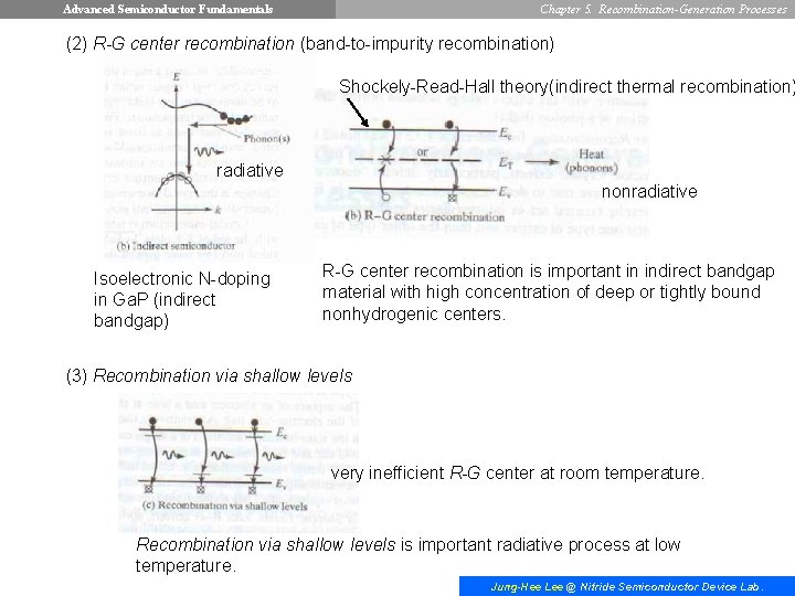
Advanced Semiconductor Fundamentals Chapter 5. Recombination-Generation Processes (2) R-G center recombination (band-to-impurity recombination) Shockely-Read-Hall theory(indirect thermal recombination) radiative nonradiative Isoelectronic N-doping in Ga. P (indirect bandgap) R-G center recombination is important in indirect bandgap material with high concentration of deep or tightly bound nonhydrogenic centers. (3) Recombination via shallow levels very inefficient R-G center at room temperature. Recombination via shallow levels is important radiative process at low temperature. Jung-Hee Lee @ Nitride Semiconductor Device Lab.
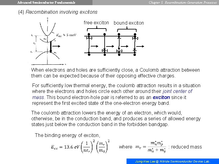
Advanced Semiconductor Fundamentals Chapter 5. Recombination-Generation Processes (4) Recombination involving excitons free exciton bound exciton When electrons and holes are sufficiently close, a Coulomb attraction between them can be expected because of their opposing effective charges. For sufficiently low thermal energy, the coulomb attraction results in a situation where the electrons and holes circle each other around their joint center of mass. This bound electron-hole pair is referred to as an exciton since it represent the first excited state of the one-electron energy band. The coulomb attraction lowers the energy of an electron, which would, otherwise, be in the conduction band, and produces a series of allowed energy states just below the conduction band in the forbidden bandgap. The binding energy of exciton, where : reduced mass Jung-Hee Lee @ Nitride Semiconductor Device Lab.
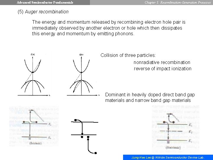
Advanced Semiconductor Fundamentals Chapter 5. Recombination-Generation Processes (5) Auger recombination The energy and momentum released by recombining electron hole pair is immediately observed by another electron or hole which then dissipates this energy and momentum by emitting phonons. Collision of three particles: nonradiative recombination reverse of impact ionization Dominant in heavily doped direct band gap materials and narrow band gap materials Jung-Hee Lee @ Nitride Semiconductor Device Lab.
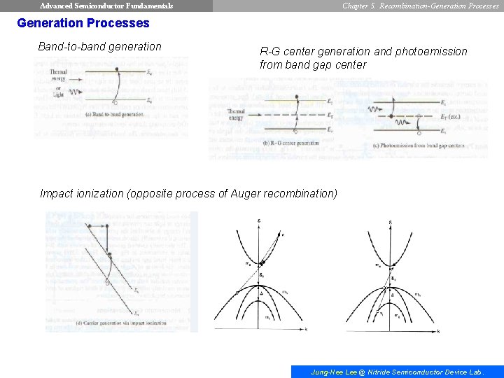
Advanced Semiconductor Fundamentals Chapter 5. Recombination-Generation Processes Band-to-band generation R-G center generation and photoemission from band gap center Impact ionization (opposite process of Auger recombination) Jung-Hee Lee @ Nitride Semiconductor Device Lab.
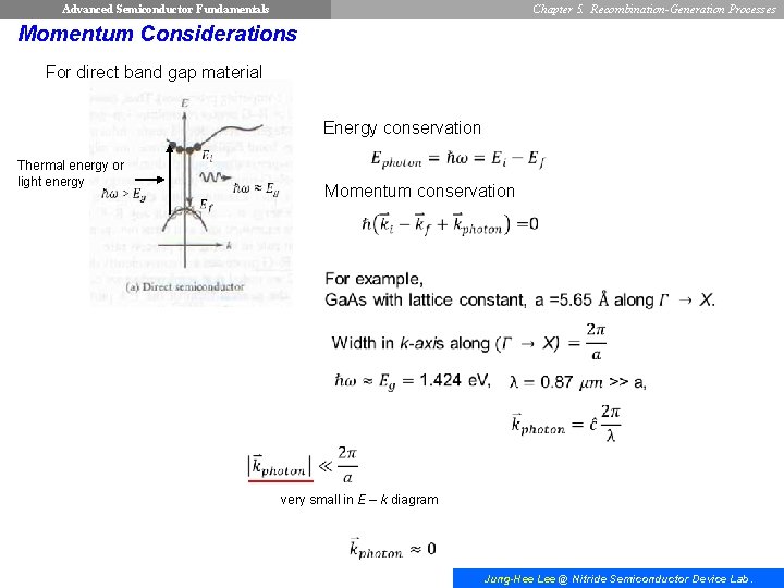
Advanced Semiconductor Fundamentals Chapter 5. Recombination-Generation Processes Momentum Considerations For direct band gap material Energy conservation Thermal energy or light energy Momentum conservation very small in E – k diagram Jung-Hee Lee @ Nitride Semiconductor Device Lab.
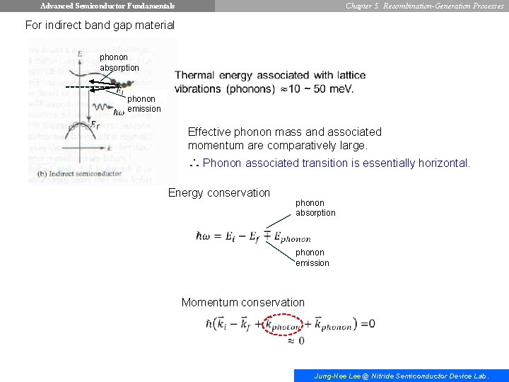
Advanced Semiconductor Fundamentals Chapter 5. Recombination-Generation Processes For indirect band gap material phonon absorption phonon emission Effective phonon mass and associated momentum are comparatively large. ∴ Phonon associated transition is essentially horizontal. Energy conservation phonon absorption phonon emission Momentum conservation Jung-Hee Lee @ Nitride Semiconductor Device Lab.
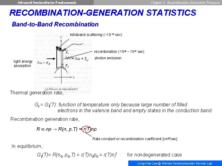
Advanced Semiconductor Fundamentals Chapter 5. Recombination-Generation Processes RECOMBINATION-GENERATION STATISTICS Band-to-Band Recombination intraband scattering (~10 -13 sec) recombination ( 10 -9 ~ 10 -6 sec) photon emission light energy absorption Thermal generation rate, Gt = Gt(T): function of temperature only because large number of filled electrons in the valence band empty states in the conduction band. Recombination generation rate, Rate constant or recombination coefficient [cm 3/sec] In equilibrium, Gt(T)= R(n 0, p 0, T) = r(T)n 0 p 0 = r(T)ni 2 for nondegenerated case Jung-Hee Lee @ Nitride Semiconductor Device Lab.
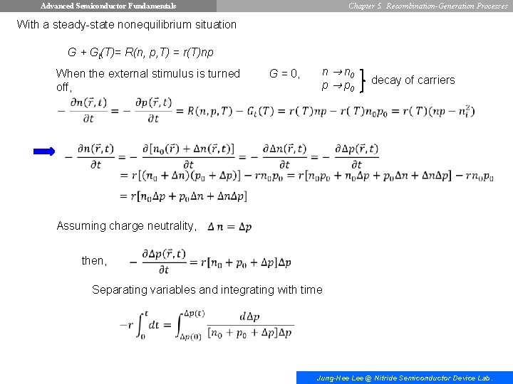
Advanced Semiconductor Fundamentals Chapter 5. Recombination-Generation Processes With a steady-state nonequilibrium situation G + Gt(T)= R(n, p, T) = r(T)np When the external stimulus is turned off, G = 0, n → n 0 p → p 0 decay of carriers Assuming charge neutrality, then, Separating variables and integrating with time Jung-Hee Lee @ Nitride Semiconductor Device Lab.
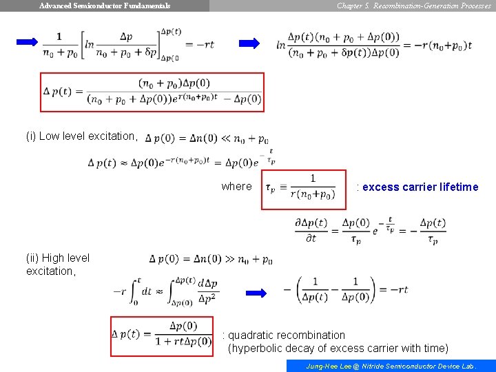
Advanced Semiconductor Fundamentals Chapter 5. Recombination-Generation Processes (i) Low level excitation, where : excess carrier lifetime (ii) High level excitation, : quadratic recombination (hyperbolic decay of excess carrier with time) Jung-Hee Lee @ Nitride Semiconductor Device Lab.
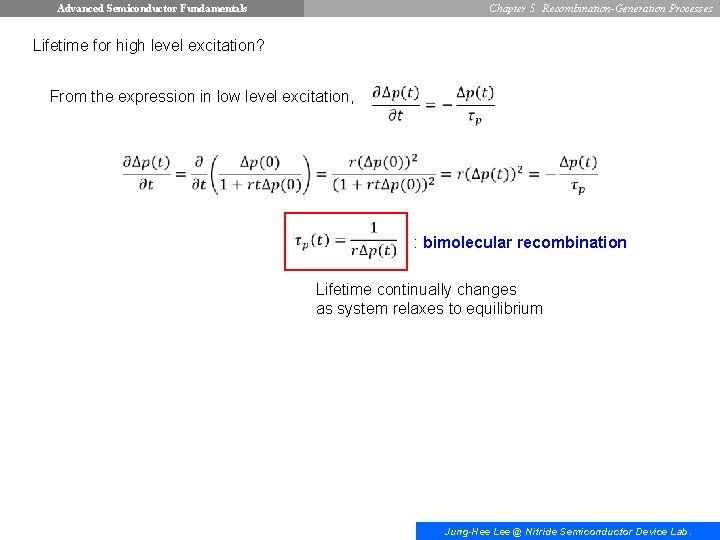
Advanced Semiconductor Fundamentals Chapter 5. Recombination-Generation Processes Lifetime for high level excitation? From the expression in low level excitation, : bimolecular recombination Lifetime continually changes as system relaxes to equilibrium Jung-Hee Lee @ Nitride Semiconductor Device Lab.
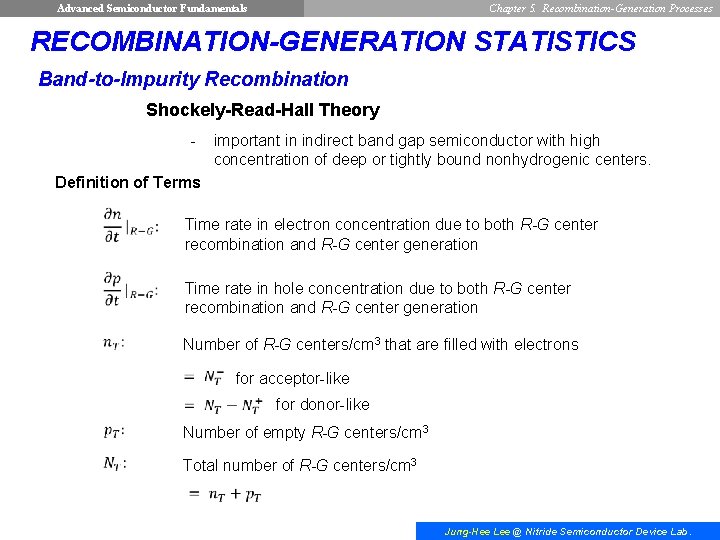
Advanced Semiconductor Fundamentals Chapter 5. Recombination-Generation Processes RECOMBINATION-GENERATION STATISTICS Band-to-Impurity Recombination Shockely-Read-Hall Theory - important in indirect band gap semiconductor with high concentration of deep or tightly bound nonhydrogenic centers. Definition of Terms Time rate in electron concentration due to both R-G center recombination and R-G center generation Time rate in hole concentration due to both R-G center recombination and R-G center generation Number of R-G centers/cm 3 that are filled with electrons for acceptor-like for donor-like Number of empty R-G centers/cm 3 Total number of R-G centers/cm 3 Jung-Hee Lee @ Nitride Semiconductor Device Lab.
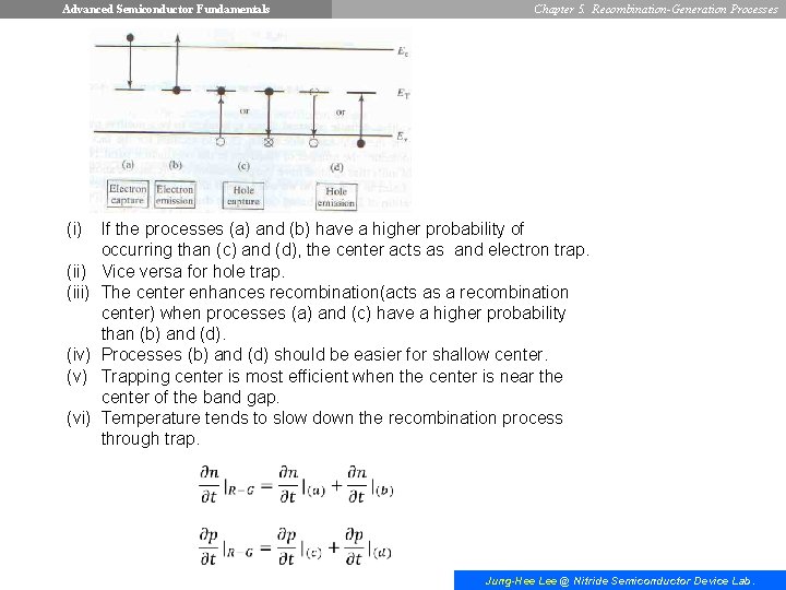
Advanced Semiconductor Fundamentals (i) (iii) (iv) (vi) Chapter 5. Recombination-Generation Processes If the processes (a) and (b) have a higher probability of occurring than (c) and (d), the center acts as and electron trap. Vice versa for hole trap. The center enhances recombination(acts as a recombination center) when processes (a) and (c) have a higher probability than (b) and (d). Processes (b) and (d) should be easier for shallow center. Trapping center is most efficient when the center is near the center of the band gap. Temperature tends to slow down the recombination process through trap. Jung-Hee Lee @ Nitride Semiconductor Device Lab.
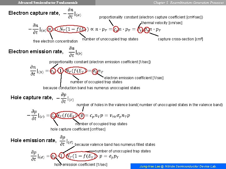
Advanced Semiconductor Fundamentals Electron capture rate, Chapter 5. Recombination-Generation Processes proportionality constant (electron capture coefficient [cm 3/sec]) thermal velocity [cm/sec] free electron concentration capture cross-section [cm 2] number of unoccupied trap states Electron emission rate, proportionality constant (electron emission coefficient [1/sec]) electron emission coefficient [1/sec] number of occupied trap states because conduction band has numerus unoccupied states Hole capture rate, number of holes in the valence band( number of unoccupied states in the valence band) number of occupied trap states hole capture coefficient [cm 3/sec] Hole emission rate, because valence band has numerus filled states number of unoccupied trap states hole emission coefficient [1/sec] Jung-Hee Lee @ Nitride Semiconductor Device Lab.
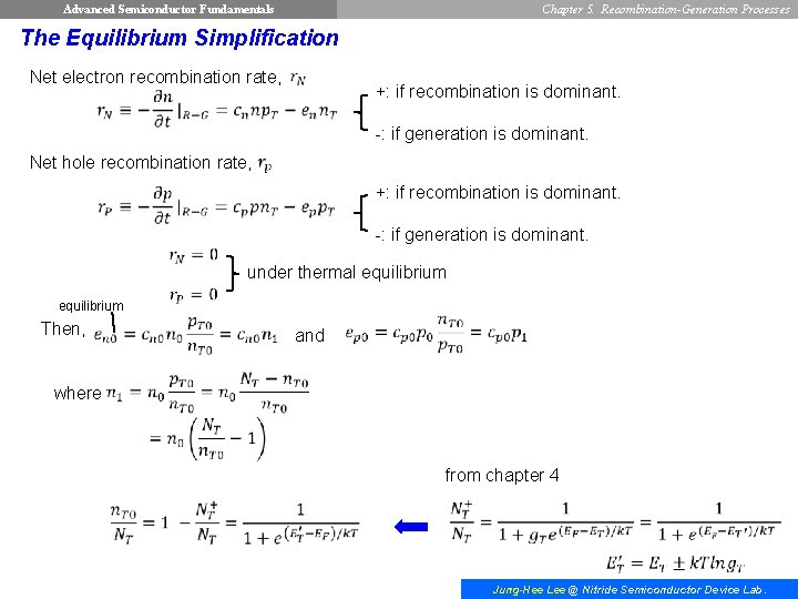
Advanced Semiconductor Fundamentals Chapter 5. Recombination-Generation Processes The Equilibrium Simplification Net electron recombination rate, +: if recombination is dominant. -: if generation is dominant. Net hole recombination rate, +: if recombination is dominant. -: if generation is dominant. under thermal equilibrium Then, and where from chapter 4 Jung-Hee Lee @ Nitride Semiconductor Device Lab.
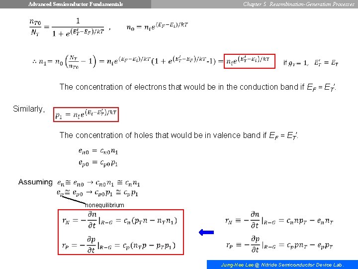
Advanced Semiconductor Fundamentals Chapter 5. Recombination-Generation Processes The concentration of electrons that would be in the conduction band if EF = ET’. Similarly, The concentration of holes that would be in valence band if EF = ET’. nonequilibrium Jung-Hee Lee @ Nitride Semiconductor Device Lab.
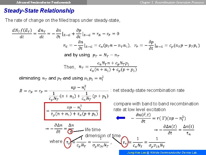
Advanced Semiconductor Fundamentals Chapter 5. Recombination-Generation Processes Steady-State Relationship The rate of change on the filled traps under steady-state, Then, : net steady-state recombination rate compare with band to band recombination rate at low level excitation life time dimension of time where Jung-Hee Lee @ Nitride Semiconductor Device Lab.
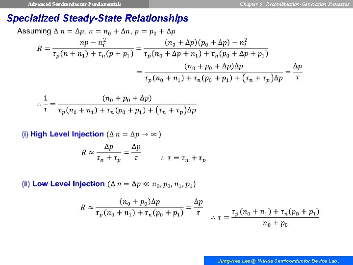
Advanced Semiconductor Fundamentals Chapter 5. Recombination-Generation Processes Specialized Steady-State Relationships Jung-Hee Lee @ Nitride Semiconductor Device Lab.
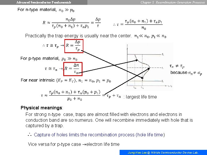
Advanced Semiconductor Fundamentals Chapter 5. Recombination-Generation Processes Practically the trap energy is usually near the center. : largest life time Physical meanings: For strong n-type case, traps are almost filled with electrons and electrons in conduction band are so numerus. One will recombine immediately with hole that is captured by a trap. ∴ Capture of holes limits the recombination process (hole life time) Vice versa for p-type case →electron life time Jung-Hee Lee @ Nitride Semiconductor Device Lab.
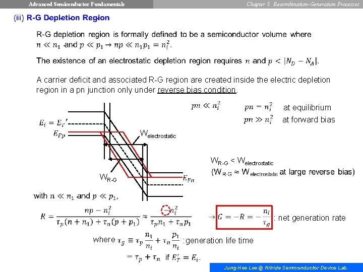
Advanced Semiconductor Fundamentals Chapter 5. Recombination-Generation Processes A carrier deficit and associated R-G region are created inside the electric depletion region in a pn junction only under reverse bias condition. at equilibrium at forward bias Welectrostatic WR-G < Welectrostatic WR-G : net generation rate where : generation life time Jung-Hee Lee @ Nitride Semiconductor Device Lab.
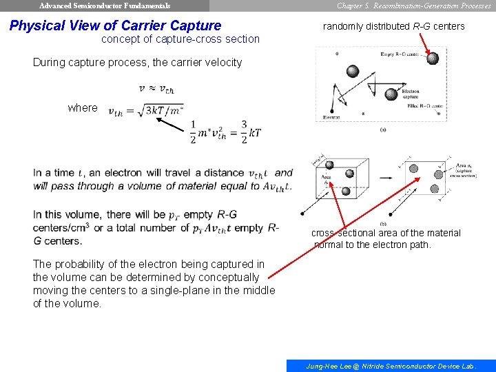
Advanced Semiconductor Fundamentals Physical View of Carrier Capture Chapter 5. Recombination-Generation Processes randomly distributed R-G centers concept of capture-cross section During capture process, the carrier velocity where cross-sectional area of the material normal to the electron path. The probability of the electron being captured in the volume can be determined by conceptually moving the centers to a single-plane in the middle of the volume. Jung-Hee Lee @ Nitride Semiconductor Device Lab.
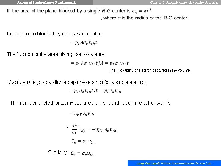
Advanced Semiconductor Fundamentals Chapter 5. Recombination-Generation Processes the total area blocked by empty R-G centers The fraction of the area giving rise to capture The probability of electron captured in the volume Capture rate (probability of capture/second) for a single electron The number of electrons/cm 3 captured per second, given n electrons/cm 3. ∴ Similarly, Jung-Hee Lee @ Nitride Semiconductor Device Lab.
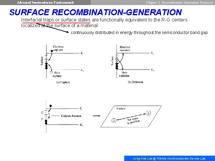
Advanced Semiconductor Fundamentals Chapter 5. Recombination-Generation Processes SURFACE RECOMBINATION-GENERATION Interfacial traps or surface states are functionally equivalent to the R-G centers localized at the surface of a material. continuously distributed in energy throughout the semiconductor band gap Jung-Hee Lee @ Nitride Semiconductor Device Lab.
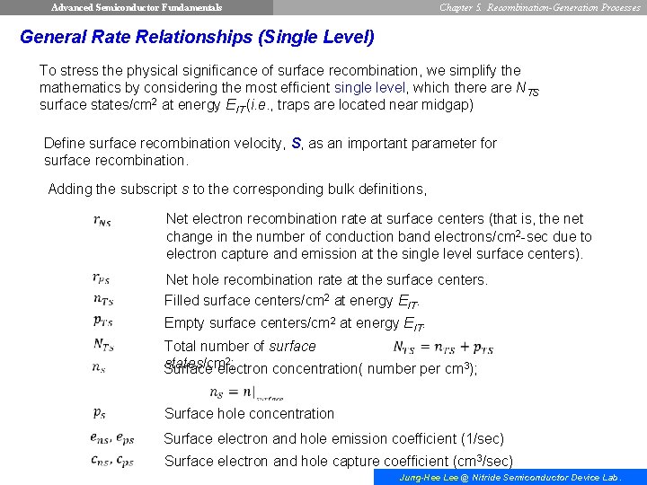
Advanced Semiconductor Fundamentals Chapter 5. Recombination-Generation Processes General Rate Relationships (Single Level) To stress the physical significance of surface recombination, we simplify the mathematics by considering the most efficient single level, which there are NTS surface states/cm 2 at energy EIT (i. e. , traps are located near midgap) Define surface recombination velocity, S, as an important parameter for surface recombination. Adding the subscript s to the corresponding bulk definitions, Net electron recombination rate at surface centers (that is, the net change in the number of conduction band electrons/cm 2 -sec due to electron capture and emission at the single level surface centers). Net hole recombination rate at the surface centers. Filled surface centers/cm 2 at energy EIT. Empty surface centers/cm 2 at energy EIT. Total number of surface 2; states/cm Surface electron concentration( number per cm 3); Surface hole concentration Surface electron and hole emission coefficient (1/sec) Surface electron and hole capture coefficient (cm 3/sec) Jung-Hee Lee @ Nitride Semiconductor Device Lab.
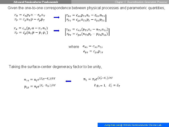
Advanced Semiconductor Fundamentals Chapter 5. Recombination-Generation Processes Given the one-to-one correspondence between physical processes and parameteric quantities, where Taking the surface-center degeneracy factor to be unity, Jung-Hee Lee @ Nitride Semiconductor Device Lab.
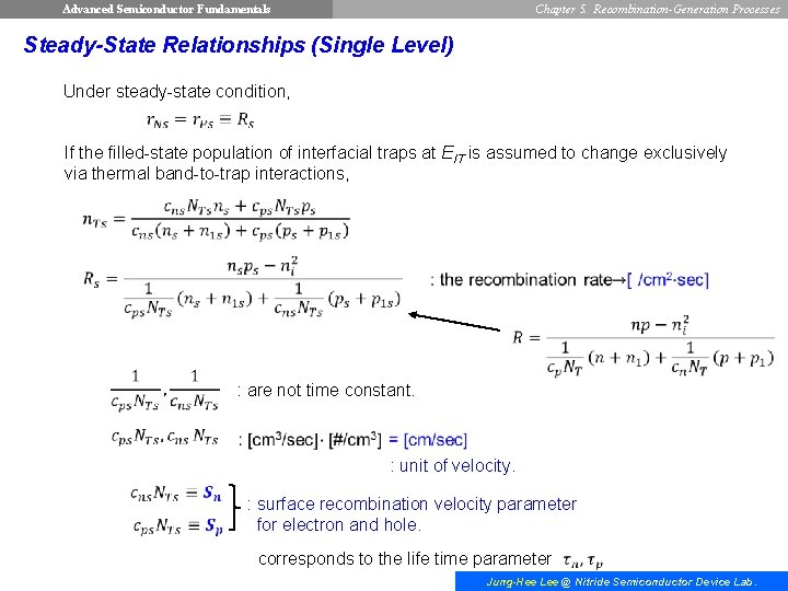
Advanced Semiconductor Fundamentals Chapter 5. Recombination-Generation Processes Steady-State Relationships (Single Level) Under steady-state condition, If the filled-state population of interfacial traps at EIT is assumed to change exclusively via thermal band-to-trap interactions, : are not time constant. : unit of velocity. : surface recombination velocity parameter for electron and hole. corresponds to the life time parameter Jung-Hee Lee @ Nitride Semiconductor Device Lab.
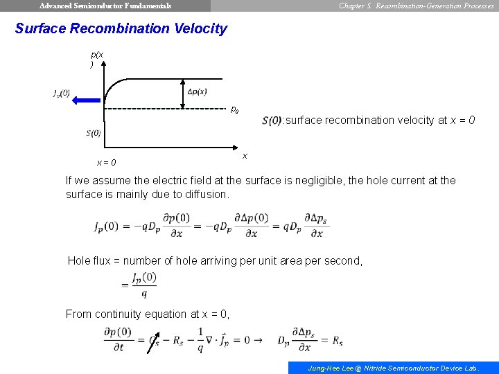
Advanced Semiconductor Fundamentals Chapter 5. Recombination-Generation Processes Surface Recombination Velocity p(x ) p 0 x=0 : surface recombination velocity at x = 0 x If we assume the electric field at the surface is negligible, the hole current at the surface is mainly due to diffusion. Hole flux = number of hole arriving per unit area per second, From continuity equation at x = 0, Jung-Hee Lee @ Nitride Semiconductor Device Lab.
![Advanced Semiconductor Fundamentals Chapter 5. Recombination-Generation Processes [cm 2/sec] (compare with unit of [cm/sec] Advanced Semiconductor Fundamentals Chapter 5. Recombination-Generation Processes [cm 2/sec] (compare with unit of [cm/sec]](http://slidetodoc.com/presentation_image_h2/1b52e7d62dc9810a95f4111ba842d948/image-29.jpg)
Advanced Semiconductor Fundamentals Chapter 5. Recombination-Generation Processes [cm 2/sec] (compare with unit of [cm/sec] In bulk) referred to as the surface recombination velocity, S. For low level excitation for n-type material, For low level excitation for p-type material, S = ~ 102 cm/sec for Si, Ge 1 ~ 10 cm/sec for oxidized Si surface 104 ~ 105 cm/sec for Ga. As To reduce surface recombination velocity in Ga. As LED, use Al. Ga. As heterostructure barrier at surface. Jung-Hee Lee @ Nitride Semiconductor Device Lab.
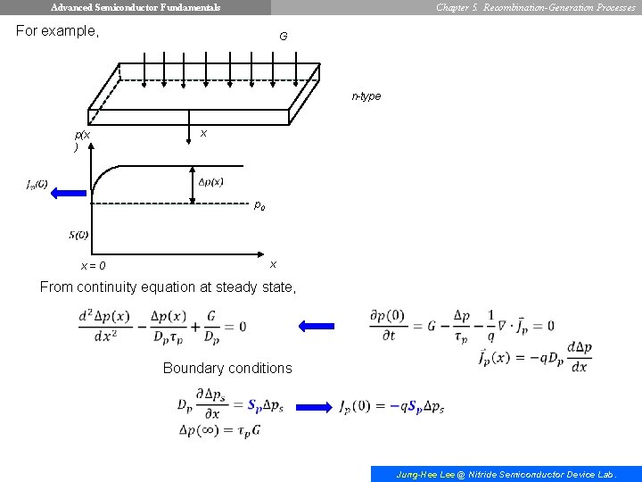
Advanced Semiconductor Fundamentals Chapter 5. Recombination-Generation Processes For example, G n-type p(x ) x p 0 x=0 x From continuity equation at steady state, Boundary conditions Jung-Hee Lee @ Nitride Semiconductor Device Lab.
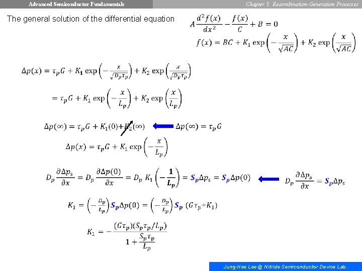
Advanced Semiconductor Fundamentals Chapter 5. Recombination-Generation Processes The general solution of the differential equation Jung-Hee Lee @ Nitride Semiconductor Device Lab.
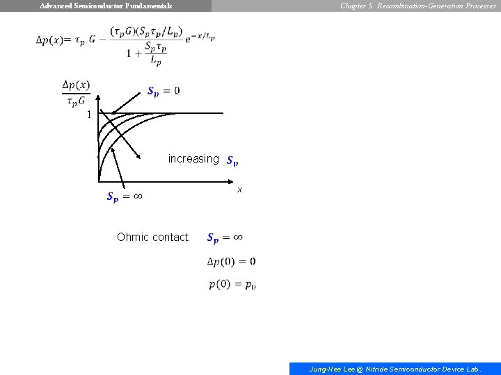
Advanced Semiconductor Fundamentals Chapter 5. Recombination-Generation Processes 1 increasing x Ohmic contact: Jung-Hee Lee @ Nitride Semiconductor Device Lab.
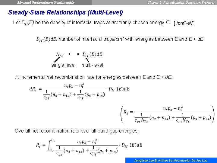
Advanced Semiconductor Fundamentals Chapter 5. Recombination-Generation Processes Steady-State Relationships (Multi-Level) Let DIT(E) be the density of interfacial traps at arbitrarily chosen energy E. : number of interfacial traps/cm 2 with energies between E and E + d. E. single level multi-level ∴ incremental net recombination rate for energies between E and E + d. E. Overall net recombination rate over all band gap energies, Jung-Hee Lee @ Nitride Semiconductor Device Lab.
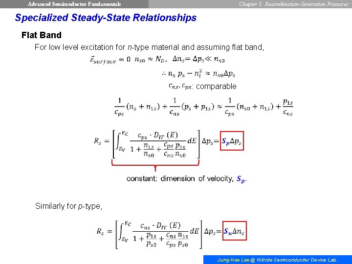
Advanced Semiconductor Fundamentals Chapter 5. Recombination-Generation Processes Specialized Steady-State Relationships Flat Band For low level excitation for n-type material and assuming flat band, : comparable Similarly for p-type, Jung-Hee Lee @ Nitride Semiconductor Device Lab.
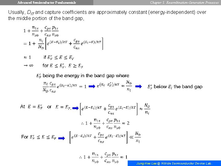
Advanced Semiconductor Fundamentals Chapter 5. Recombination-Generation Processes Usually, DIT and capture coefficients are approximately constant (energy-independent) over the middle portion of the band gap, Jung-Hee Lee @ Nitride Semiconductor Device Lab.
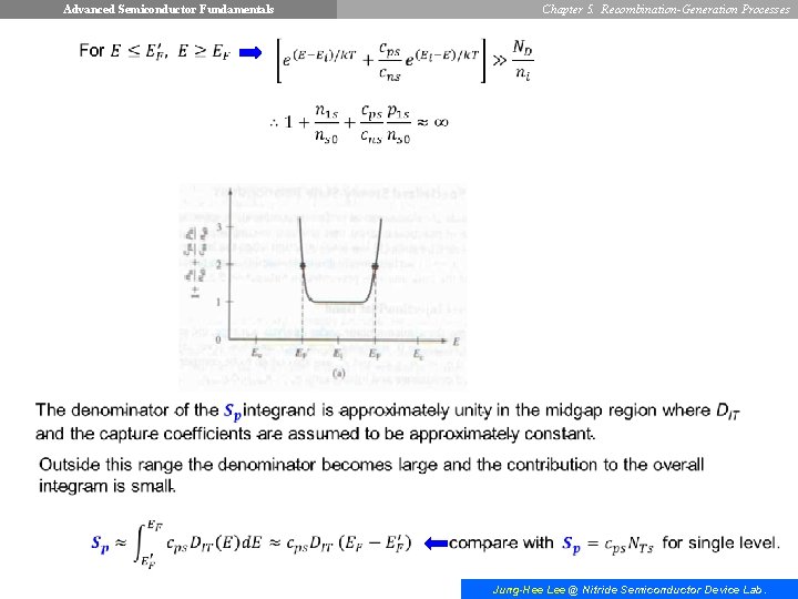
Advanced Semiconductor Fundamentals Chapter 5. Recombination-Generation Processes Jung-Hee Lee @ Nitride Semiconductor Device Lab.
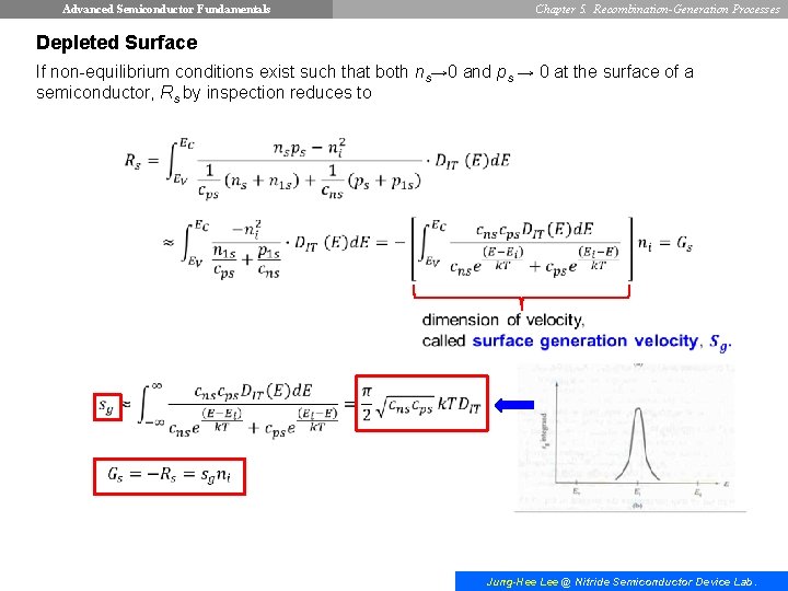
Advanced Semiconductor Fundamentals Chapter 5. Recombination-Generation Processes Depleted Surface If non-equilibrium conditions exist such that both ns→ 0 and ps → 0 at the surface of a semiconductor, Rs by inspection reduces to Jung-Hee Lee @ Nitride Semiconductor Device Lab.
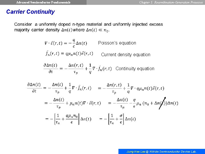
Advanced Semiconductor Fundamentals Chapter 5. Recombination-Generation Processes Carrier Continuity Poisson’s equation Current density equation Continuity equation Jung-Hee Lee @ Nitride Semiconductor Device Lab.
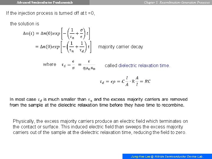
Advanced Semiconductor Fundamentals Chapter 5. Recombination-Generation Processes If the injection process is turned off at t =0, the solution is majority carrier decay where called dielectric relaxation time. Physically, the excess majority carriers produce an electric field which terminates on the contact or surface. This induced electric field than sweeps the excess majority carriers out of the sample at the dielectric relaxation time, reducing the field to zero. Jung-Hee Lee @ Nitride Semiconductor Device Lab.
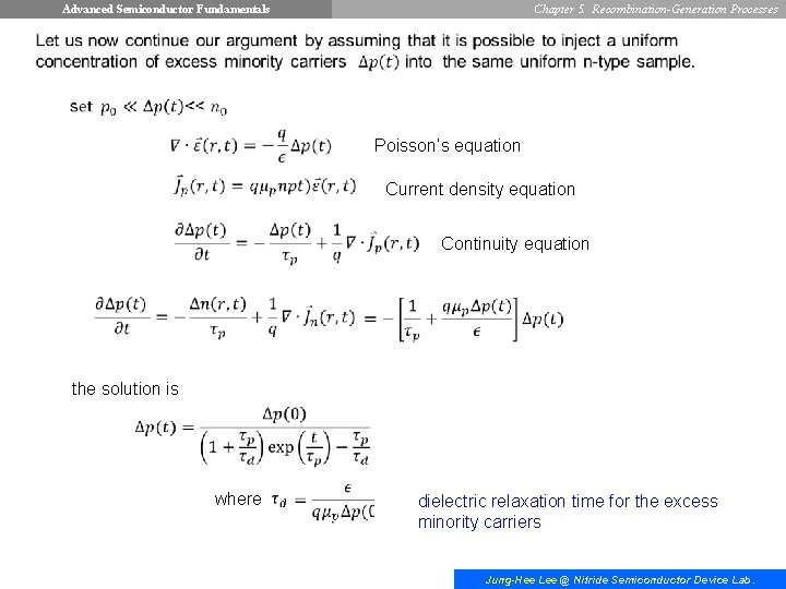
Advanced Semiconductor Fundamentals Chapter 5. Recombination-Generation Processes Poisson’s equation Current density equation Continuity equation the solution is where dielectric relaxation time for the excess minority carriers Jung-Hee Lee @ Nitride Semiconductor Device Lab.
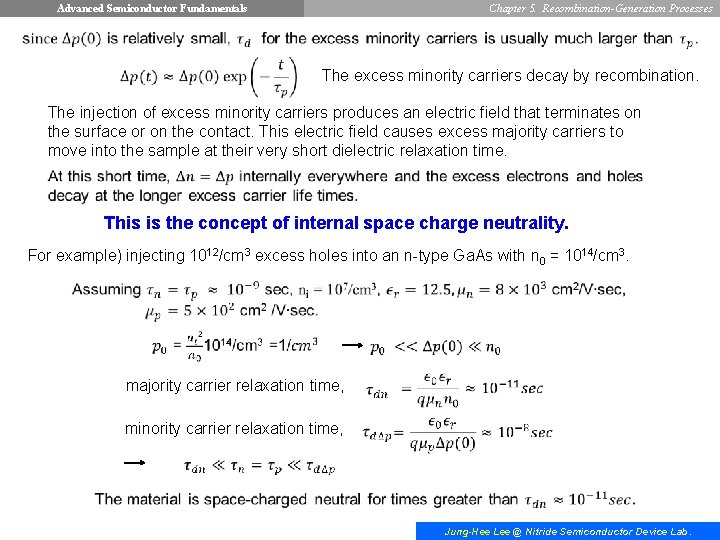
Advanced Semiconductor Fundamentals Chapter 5. Recombination-Generation Processes The excess minority carriers decay by recombination. The injection of excess minority carriers produces an electric field that terminates on the surface or on the contact. This electric field causes excess majority carriers to move into the sample at their very short dielectric relaxation time. This is the concept of internal space charge neutrality. For example) injecting 1012/cm 3 excess holes into an n-type Ga. As with n 0 = 1014/cm 3. majority carrier relaxation time, minority carrier relaxation time, Jung-Hee Lee @ Nitride Semiconductor Device Lab.
- Slides: 41