Advanced microfabrication 2017 Serial writing pattern generation sami

Advanced microfabrication 2017 Serial writing & pattern generation sami. franssila@aalto. fi

Generation vs. replication • Generation: how to achieve the very first image (in old time photography: how to create the image and fix it on film) • Replication of mask pattern on another substrate (in photography, making prints of the original negatives)
 • electron beams • ion beams • SPM-type systems nano, top")
Pattern generation (PG) • electron beams • ion beams • SPM-type systems nano, top down • laser beams • lamps & mirror • ink jets & sprayers micro, top down • colloidal litho • block co-polymer patterns bottom up • direct writing structure of final material directly

Lamp & stage PG illumination from Hg-lamp exposed resist aperture blade stage movement

Laser PG laser beam piezo translator lens piezotranslator mask plate vacuum chuck x-stage y-stage feedback circuitry interferometer mirror

Raster scan vs. vector scan Raster scan: exposure / no exposure decision at each pixel Vector scan: intelligent skipping of empty spaces

Electron beam lithography • • serial writing of each pixel high resolution slow speed thin resist for good resolution

Electron beam spot size • Beam spots in the 5 nm range are available. ( = 8 pm for 25 k. V electrons !! ) • Limited by electron source size and electron optics aberrations and diffraction for highly collimated beams. • Interactions in solid further limit minimum size: effective beam diameter is given by • deff (nm) = 0. 9 (t/V)1. 5 resist thickness t is in nm and voltage in k. V. • deff = 28 nm for 200 nm thick resist at 20 k. V

Electron scattering in resist 50 k. V 10 k. V a b 50 k. V 10 k. V c d Minimize scattering effects by using: • higher energy ( heating, charging) • thinner resist ( etch resistance limited)

Larger areas by EBL Mechanical stage scan to pattern larger areas Beam stepping to cover main field Beam deflection over subfield
 • beam spot size in")
Limitations in EBL • electron beam diameter (Coulomb; aberrations) • beam spot size in resist (thickness, forward scattering) • proximity effect (backscattering; substrate dependent) • sensitivity-resolution trade-off (low sensitivity high resolution) • dose vs. feature size relation (not a flat function) • resist thickness (etch resistance; lift-off) • substrate heating (quartz vs. silicon; pattern density)

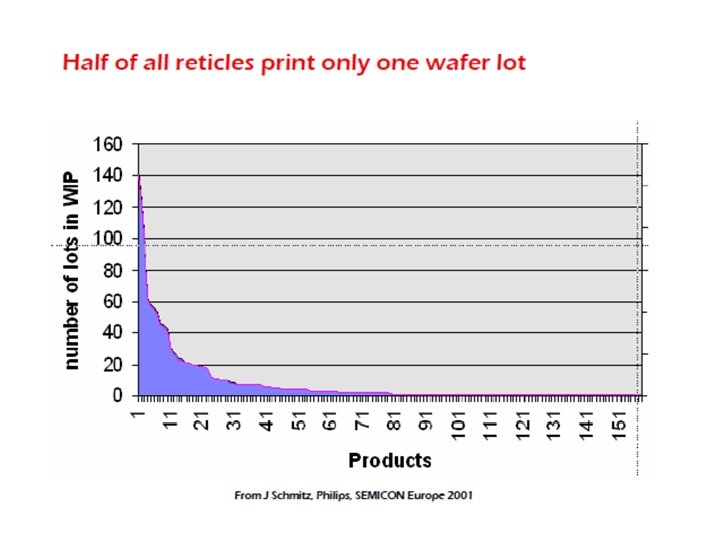
Mask making • The most voluminous application of general purpose pattern generation is to make masks for optical lithography • (electron) beam writing slow (1 000 pixels/second requires 10 M€ tools) • optical replication fast (1 000 000 pixels exposed in a second with 100 000€ tool) (10 hours vs. 1 second per wafer !)

Mask making process flow Mask blank preparation deposition of chrome on quartz resist application Pattern writing e-beam or laser Pattern processing resist development chrome etching resist stripping Metrology CD (critical dimension) control Inspection for pattern integrity defects (in chrome) pattern fidelity (shape and position) Cleaning particle removal Repair focussed ion beam etching and/or deposition Final defect inspection

Mask defects bridging necking protrusion pinhole intrusion pinspot
 Where do the particles land ? Mask designs have different sensitivity")
Mask defects (2) Where do the particles land ? Mask designs have different sensitivity to particle defects.
 Soft defects: can be cleaned away (e. g. resist residue) Hard")
Mask defects (3) Soft defects: can be cleaned away (e. g. resist residue) Hard defects: permanent (e. g. scratch in chrome) Aesthetic defects: non-critical to device performance (e. g. chrome color or spots/holes in non-device area) Optical defects not related to written patterns include: -transmission variability in glass (LF areas) -transmission variability in chrome (DF areas)

Micromirror pattern generation
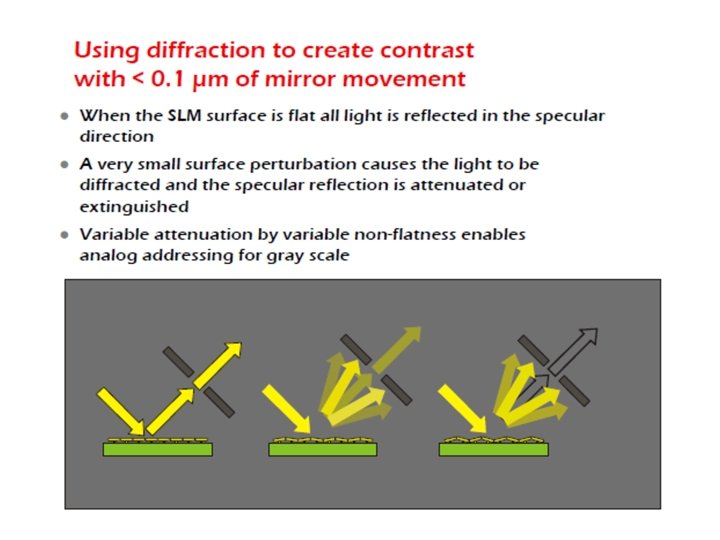

Micro mirror devices
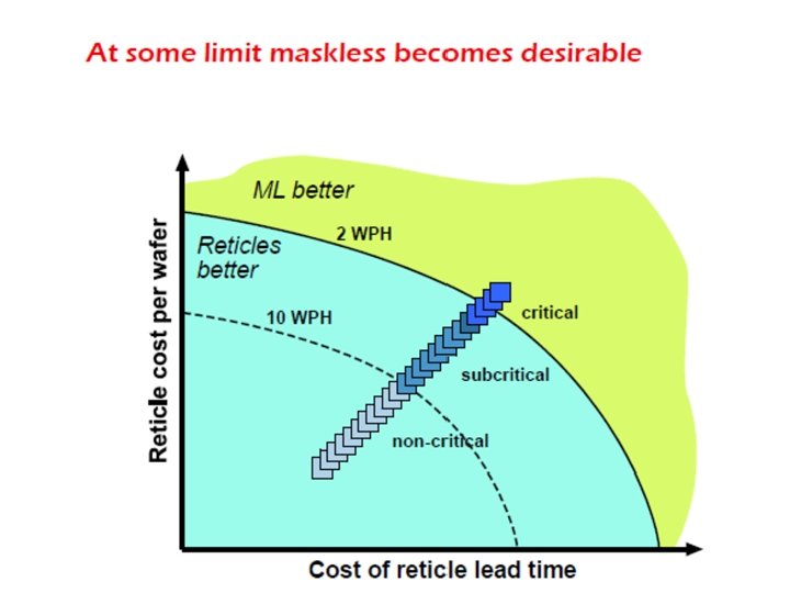

Optical lithography vs. beam writing • optical lithography with masks is the main method both in production and R&D • fixed costs rise exponentially as linewidths are scaled down: mask sets cost 1 -2 M$ for 22 nm CMOS • beam writing methods have quick turnaround time (design-to-first-chip) • beam writing eliminates mask cost • beam writing is too slow for production

Ion beam lithography Basic ideas similar to e-beam Differences: Ions heavier than electrons less scattering Resist sensitivity to ions different smaller doses suffice Ion optics bulkier more expensive systems

Half-time

Scanning probe litho
")
Scanning probe litho (2)

Colloidal lithography ≈ nanobead lithography

Block co-polymer litho
")
Block co-polymer litho (2)
")
Direct writing ≈ Maskless lithography 1: direct writing as a synonym for pixel-bypixel (beam) writing, as opposed to optical lithography and imprinting which use a photomask or mould as an intermediate step 2: direct writing as a method which skips the intermediate resist step and produces the final structure of desired material
 etching Gallium ions sputter erode the substrate (ion beam etching/milling);")
Focussed Ion Beam (FIB) etching Gallium ions sputter erode the substrate (ion beam etching/milling); Secondary electrons emitted enable (electron) microscopy to be carried out in-situ. Utke, I. , P. Hoffmann & J. Melngailis: Gas-assisted focused electron beam and ion beam processing and fabrication, J. Vac. Sci. Technol. B 26 (2008) pp. 1197 -1276

FIB systems Price tag: 1 - 5 M€

FIB machining Antti Peltonen, Aalto

FIB & DRIE plasma etching FIB surface modification Si: Ga surface resistant to etching DRIE of underlying silicon N Chekurov, K Grigoras, A Peltonen, S Franssila and I Tittonen, Nanotechnology 20 (2009) 065307 (5 pp)
; or supply energy")
FIB deposition Gallium ions sputter erode the substrate (ion beam etching/milling); or supply energy to (CVD) film deposition W(CO)6 (g) ==> W (s) + 6 CO (g) Secondary electrons emitted enable (electron) microscopy to be carried out in-situ.
 p.")
3 D deposition/etching possible T. Fujii et al: J. Micromech. Microeng. 15 (2005) p. S 286

FEB=Focussed Electron Beam Electron-beam induced chemical reactions lead to deposition Utke, I. , P. Hoffmann & J. Melngailis: Gas-assisted focused electron beam and ion beam processing and fabrication, J. Vac. Sci. Technol. B 26 (2008) pp. 1197 -1276

E-beam induced deposition Rangelow, I. W. Utke, I. , P. Hoffmann & J. Melngailis: Gas-assisted focused electron beam and ion beam processing and fabrication, J. Vac. Sci. Technol. B 26 (2008) pp. 1197 -1276

Nanofrazor: Local evaporation of resist using a heated tip

2 photon photopolymerization

2 PP

Processing after colloidal litho Colloidal Lithography By Ye Yu and Gang Zhang
")
Processing after colloidal litho (2)

Processing after BCP litho
")
Processing after BCP litho (2)
- Slides: 45