Advanced Materials and Structures for Nanoscale CMOS Prof
- Slides: 43

Advanced Materials and Structures for Nanoscale CMOS Prof. Tsu-Jae King Department of Electrical Engineering and Computer Sciences University of California, Berkeley, CA 94720 -1770 USA March 29, 2004 FLCC Seminar

Outline • Introduction – MOSFET scaling • Advanced Gate-Stack Materials • Thin-Body MOSFETs • Summary T. -J. King -2 - March 29, 2004

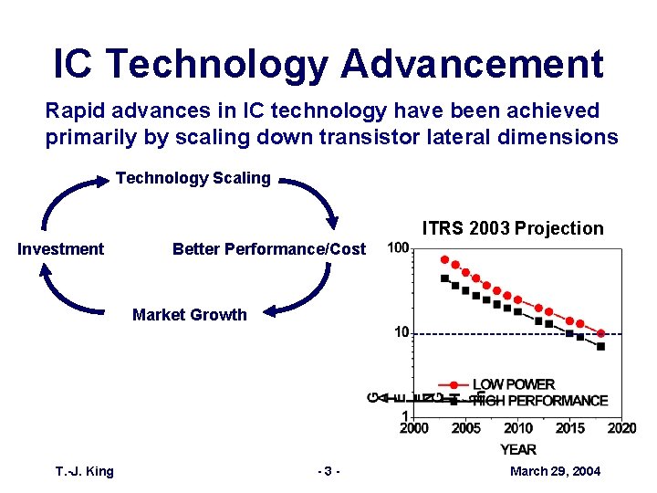
IC Technology Advancement Rapid advances in IC technology have been achieved primarily by scaling down transistor lateral dimensions Technology Scaling ITRS 2003 Projection Investment Better Performance/Cost Market Growth T. -J. King -3 - March 29, 2004

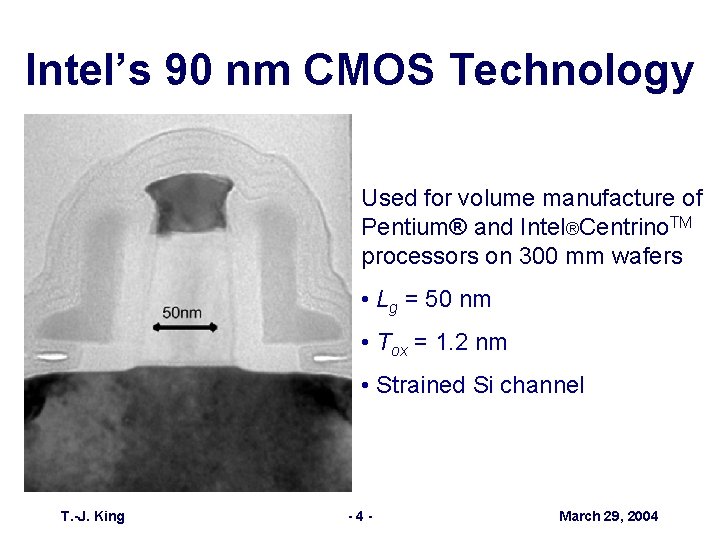
Intel’s 90 nm CMOS Technology Used for volume manufacture of Pentium® and Intel®Centrino. TM processors on 300 mm wafers • Lg = 50 nm • Tox = 1. 2 nm • Strained Si channel T. -J. King -4 - March 29, 2004

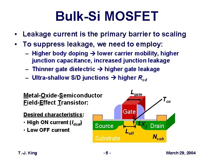
Bulk-Si MOSFET • Leakage current is the primary barrier to scaling • To suppress leakage, we need to employ: – Higher body doping lower carrier mobility, higher junction capacitance, increased junction leakage – Thinner gate dielectric higher gate leakage – Ultra-shallow S/D junctions higher Rsd Lgate Metal-Oxide-Semiconductor Field-Effect Transistor: Desired characteristics: • High ON current (Idsat) • Low OFF current Gate Source Substrate T. -J. King Tox -5 - Leff Xj Drain Nsub March 29, 2004

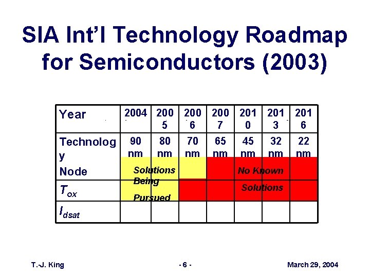
SIA Int’l Technology Roadmap for Semiconductors (2003) Year Technolog y Node Tox 2004 200 5 90 nm 80 nm 200 6 200 7 201 0 201 3 201 6 70 nm 65 nm 45 nm 32 nm 22 nm Solutions Being No Known Solutions Pursued Idsat T. -J. King -6 - March 29, 2004

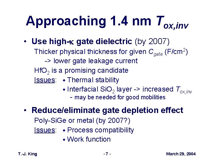
Approaching 1. 4 nm Tox, inv • Use high-k gate dielectric (by 2007) Thicker physical thickness for given Cgate (F/cm 2) -> lower gate leakage current Hf. O 2 is a promising candidate Issues: Thermal stability Interfacial Si. O 2 layer -> increased Tox, inv - may be needed for good mobilities • Reduce/eliminate gate depletion effect Poly-Si. Ge or metal (by 2007? ) Issues: Process compatibility Work function T. -J. King -7 - March 29, 2004

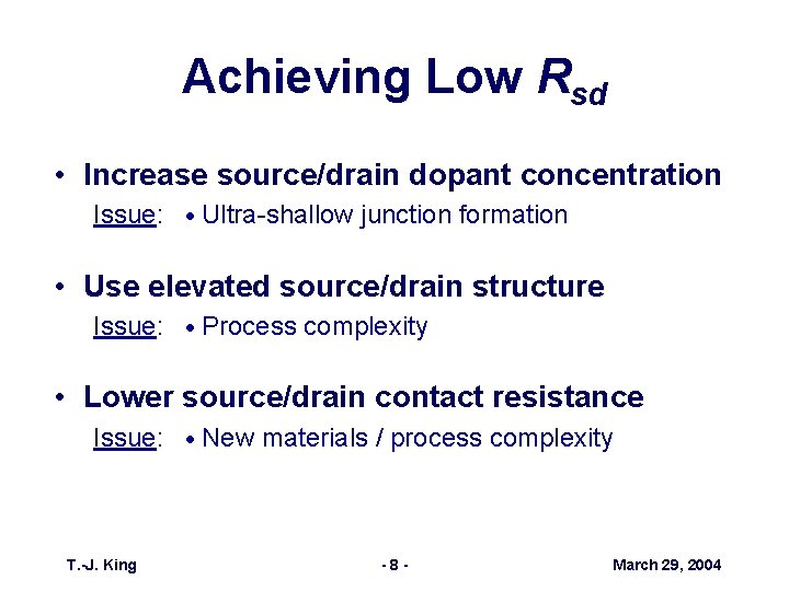
Achieving Low Rsd • Increase source/drain dopant concentration Issue: Ultra-shallow junction formation • Use elevated source/drain structure Issue: Process complexity • Lower source/drain contact resistance Issue: New materials / process complexity T. -J. King -8 - March 29, 2004

Outline • Introduction • Advanced Gate-Stack Materials – Poly-Si. Ge gate electrode – Mo gate electrode • Thin-Body MOSFETs • Summary T. -J. King -9 - March 29, 2004

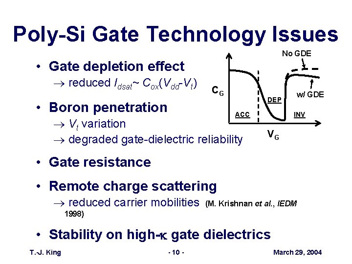
Poly-Si Gate Technology Issues No GDE • Gate depletion effect ® reduced Idsat~ Cox(Vdd-Vt) CG • Boron penetration w/ GDE DEP ACC ® Vt variation ® degraded gate-dielectric reliability INV VG • Gate resistance • Remote charge scattering ® reduced carrier mobilities (M. Krishnan et al. , IEDM 1998) • Stability on high-k gate dielectrics T. -J. King - 10 - March 29, 2004

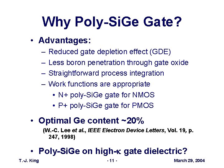
Why Poly-Si. Ge Gate? • Advantages: – – Reduced gate depletion effect (GDE) Less boron penetration through gate oxide Straightforward process integration Work functions are appropriate • N+ poly-Si. Ge gate for NMOS • P+ poly-Si. Ge gate for PMOS • Optimal Ge content ~20% (W. -C. Lee et al. , IEEE Electron Device Letters, Vol. 19, p. 247, 1998) • Poly-Si. Ge on high-k gate dielectric? T. -J. King - 11 - March 29, 2004

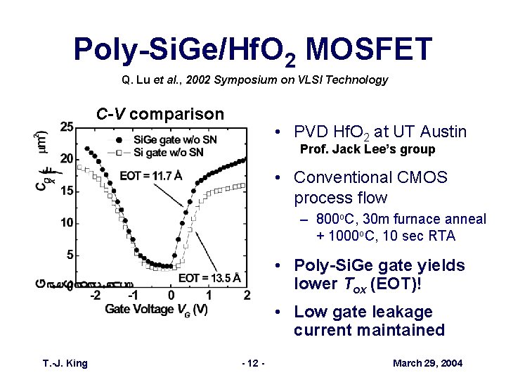
Poly-Si. Ge/Hf. O 2 MOSFET Q. Lu et al. , 2002 Symposium on VLSI Technology C-V comparison • PVD Hf. O 2 at UT Austin Prof. Jack Lee’s group • Conventional CMOS process flow – 800 o. C, 30 m furnace anneal + 1000 o. C, 10 sec RTA • Poly-Si. Ge gate yields lower Tox (EOT)! • Low gate leakage current maintained T. -J. King - 12 - March 29, 2004

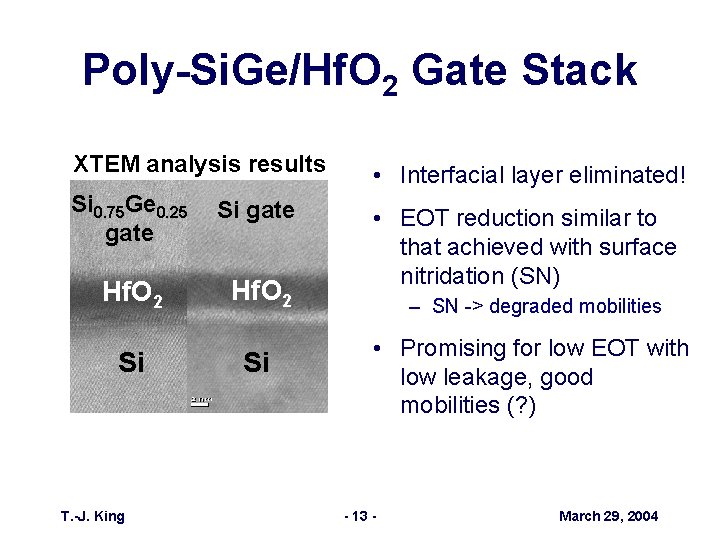
Poly-Si. Ge/Hf. O 2 Gate Stack XTEM analysis results Si 0. 75 Ge 0. 25 gate Si gate Hf. O 2 Si T. -J. King Si • Interfacial layer eliminated! • EOT reduction similar to that achieved with surface nitridation (SN) – SN -> degraded mobilities • Promising for low EOT with low leakage, good mobilities (? ) - 13 - March 29, 2004

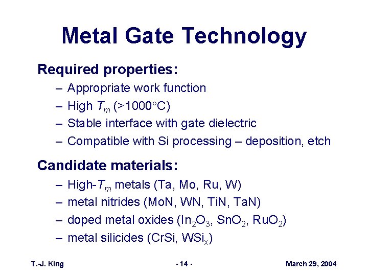
Metal Gate Technology Required properties: – – Appropriate work function High Tm (>1000 C) Stable interface with gate dielectric Compatible with Si processing – deposition, etch Candidate materials: – – T. -J. King High-Tm metals (Ta, Mo, Ru, W) metal nitrides (Mo. N, WN, Ti. N, Ta. N) doped metal oxides (In 2 O 3, Sn. O 2, Ru. O 2) metal silicides (Cr. Si, WSix) - 14 - March 29, 2004

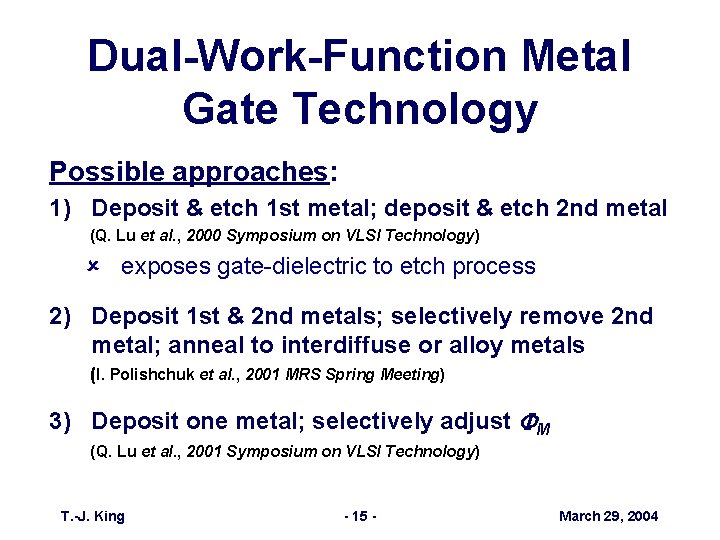
Dual-Work-Function Metal Gate Technology Possible approaches: 1) Deposit & etch 1 st metal; deposit & etch 2 nd metal (Q. Lu et al. , 2000 Symposium on VLSI Technology) û exposes gate-dielectric to etch process 2) Deposit 1 st & 2 nd metals; selectively remove 2 nd metal; anneal to interdiffuse or alloy metals (I. Polishchuk et al. , 2001 MRS Spring Meeting) 3) Deposit one metal; selectively adjust FM (Q. Lu et al. , 2001 Symposium on VLSI Technology) T. -J. King - 15 - March 29, 2004

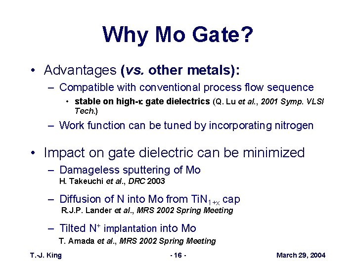
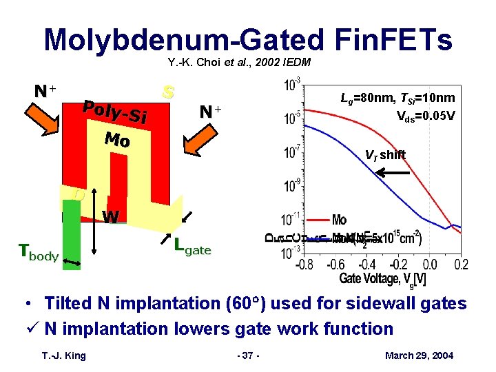
Why Mo Gate? • Advantages (vs. other metals): – Compatible with conventional process flow sequence • stable on high-k gate dielectrics (Q. Lu et al. , 2001 Symp. VLSI Tech. ) – Work function can be tuned by incorporating nitrogen • Impact on gate dielectric can be minimized – Damageless sputtering of Mo H. Takeuchi et al. , DRC 2003 – Diffusion of N into Mo from Ti. N 1+x cap R. J. P. Lander et al. , MRS 2002 Spring Meeting – Tilted N+ implantation into Mo T. Amada et al. , MRS 2002 Spring Meeting T. -J. King - 16 - March 29, 2004

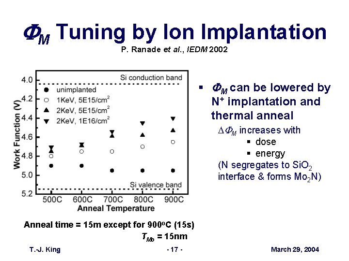
FM Tuning by Ion Implantation P. Ranade et al. , IEDM 2002 § FM can be lowered by N+ implantation and thermal anneal DFM increases with § dose § energy (N segregates to Si. O 2 interface & forms Mo 2 N) Anneal time = 15 m except for 900 o. C (15 s) TMo = 15 nm T. -J. King - 17 - March 29, 2004

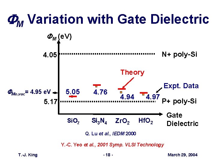
FM Variation with Gate Dielectric FM (e. V) N+ poly-Si 4. 05 Theory FMo, vac= 4. 95 e. V 5. 05 4. 76 5. 17 Si. O 2 Si 3 N 4 Expt. Data 4. 94 Zr. O 2 4. 97 P+ poly-Si Hf. O 2 Gate Dielectric Q. Lu et al. , IEDM 2000 Y. -C. Yeo et al. , 2001 Symp. VLSI Technology T. -J. King - 18 - March 29, 2004

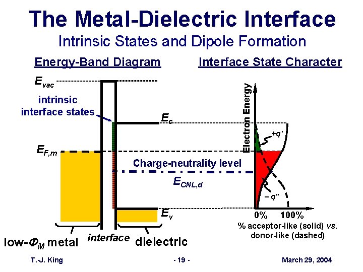
The Metal-Dielectric Interface Intrinsic States and Dipole Formation Interface State Character Energy-Band Diagram intrinsic interface states Electron Energy Evac Ec EF, m Charge-neutrality level +q’ _ ECNL, d – q” Ev 0% low-FM metal interface dielectric T. -J. King - 19 - 100% % acceptor-like (solid) vs. donor-like (dashed) March 29, 2004

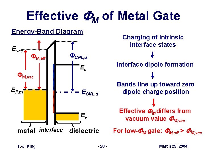
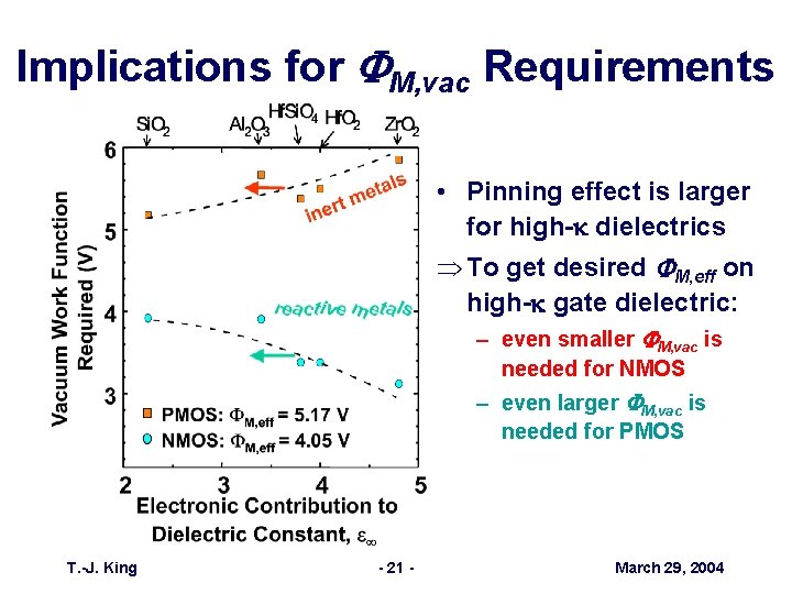
Effective FM of Metal Gate Energy-Band Diagram Evac FM, eff FM, vac EF, m Charging of intrinsic interface states FCNL, d Interface dipole formation Ec ECNL, d Effective FM differs from vacuum value FM, vac Ev metal interface dielectric T. -J. King Bands line up toward zero dipole charge position - 20 - For low-FM gate: FM, eff > FM, vac March 29, 2004

Implications for FM, vac Requirements • Pinning effect is larger for high-k dielectrics Þ To get desired FM, eff on high-k gate dielectric: – even smaller FM, vac is needed for NMOS – even larger FM, vac is needed for PMOS T. -J. King - 21 - March 29, 2004

Outline • Introduction • Advanced Gate-Stack Materials • Thin-Body MOSFETs – Ultra-thin body – Double-gate • Summary T. -J. King - 22 - March 29, 2004

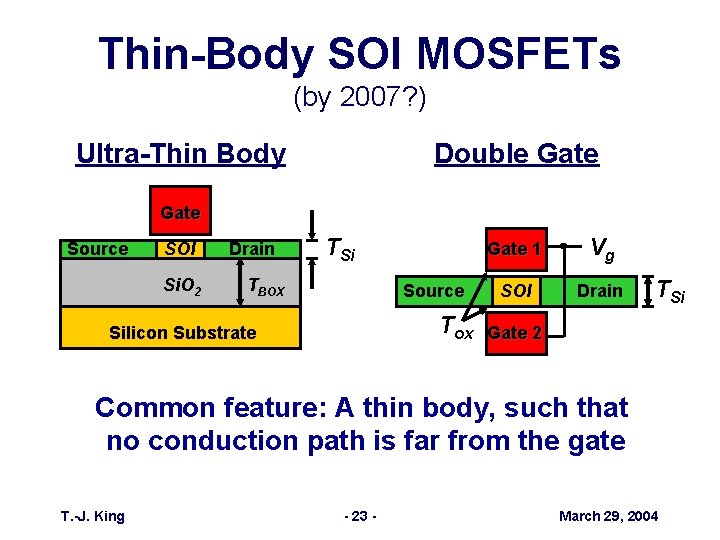
Thin-Body SOI MOSFETs (by 2007? ) Ultra-Thin Body Double Gate Source SOI Si. O 2 Drain TSi TBOX Source Tox Silicon Substrate Gate 1 Vg SOI Drain TSi Gate 2 Common feature: A thin body, such that no conduction path is far from the gate T. -J. King - 23 - March 29, 2004

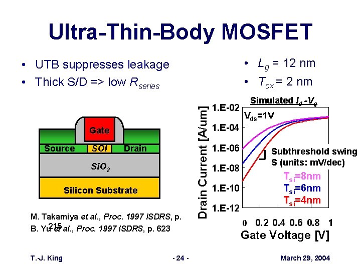
Ultra-Thin-Body MOSFET • Lg = 12 nm • UTB suppresses leakage • Thick S/D => low Rseries Gate Source SOI Drain Si. O 2 Silicon Substrate M. Takamiya et al. , Proc. 1997 ISDRS, p. B. Yu 215 et al. , Proc. 1997 ISDRS, p. 623 T. -J. King - 24 - Drain Current [A/um] • Tox = 2 nm 1. E-02 Simulated Id -Vg Vds=1 V 1. E-04 1. E-06 1. E-08 1. E-10 1. E-12 Subthreshold swing S (units: m. V/dec) Tsi=8 nm Tsi=6 nm Tsi=4 nm 0 0. 2 0. 4 0. 6 0. 8 1 Gate Voltage [V] March 29, 2004

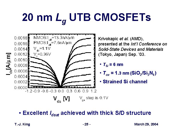
20 nm Lg UTB CMOSFETs Krivokapic et al. (AMD), presented at the Int’l Conference on Solid-State Devices and Materials (Tokyo, Japan) Sep. ’ 03. • TSi = 6 nm • Tox = 1. 3 nm (Si. O 2/Si 3 N 4) • Strained Si channel • Excellent Idsat achieved with thick S/D structure T. -J. King - 25 - March 29, 2004

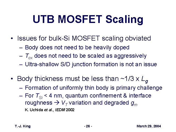
UTB MOSFET Scaling • Issues for bulk-Si MOSFET scaling obviated – Body does not need to be heavily doped – Tox does not need to be scaled as aggressively – Ultra-shallow S/D junction formation is not an issue • Body thickness must be less than ~1/3 x Lg – Formation of uniformly thin body is primary challenge – For TSi < 4 nm, quantum confinement & interface roughness VT variation and degraded gm K. Uchida et al. , IEDM 2002 T. -J. King - 26 - March 29, 2004

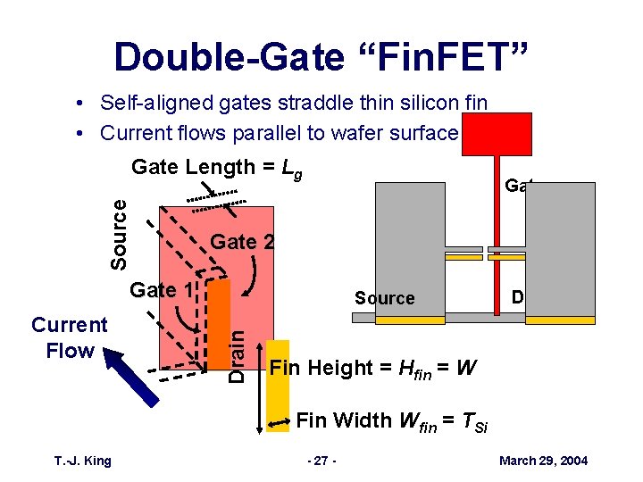
Double-Gate “Fin. FET” • Self-aligned gates straddle thin silicon fin • Current flows parallel to wafer surface Source Gate Length = Lg Gate 2 Gate 1 Drain Current Flow Source Drain Fin Height = Hfin = W Fin Width Wfin = TSi T. -J. King - 27 - March 29, 2004

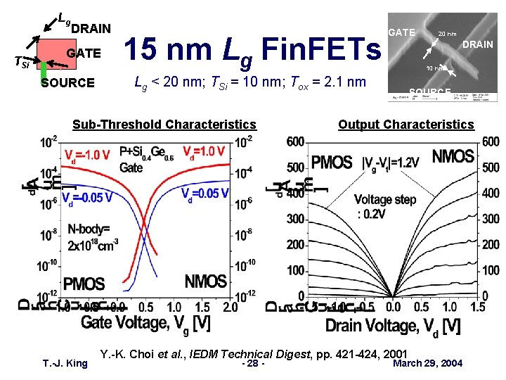
Lg TSi DRAIN GATE SOURCE 15 nm Lg Fin. FETs 10 nm SOURCE Output Characteristics Y. -K. Choi et al. , IEDM Technical Digest, pp. 421 -424, 2001 - 28 - 20 nm DRAIN Lg < 20 nm; TSi = 10 nm; Tox = 2. 1 nm Sub-Threshold Characteristics T. -J. King GATE March 29, 2004

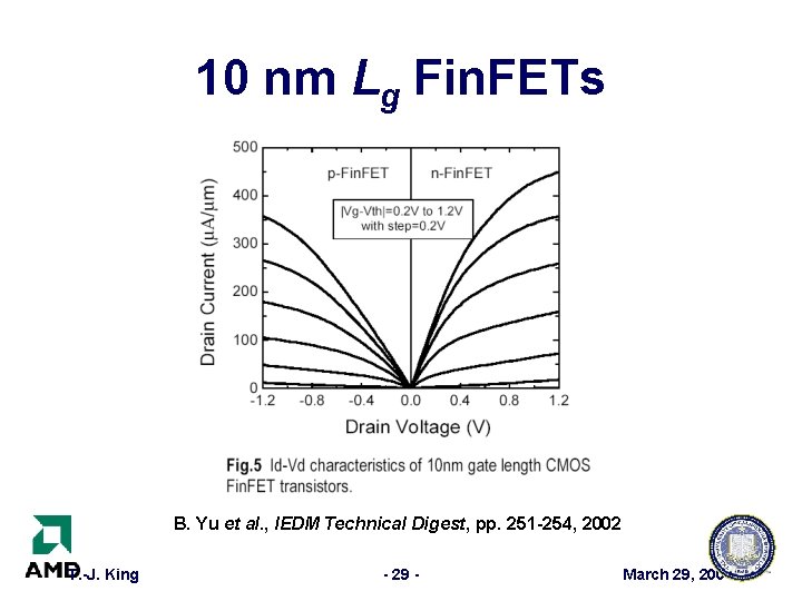
10 nm Lg Fin. FETs B. Yu et al. , IEDM Technical Digest, pp. 251 -254, 2002 T. -J. King - 29 - March 29, 2004

Fin. FET Scaling • Compared with UTB-MOSFET: – Reduced short-channel effects => more scalable – Higher current drive due to • steeper subthreshold swing (60 m. V/dec) • lower channel electric field => higher carrier mobilities • Fin width must be less than 2/3 x Lgate Formation of narrow fin is primary challenge • sub-lithographic process needed T. -J. King - 30 - March 29, 2004

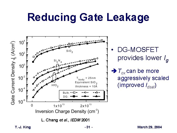
Reducing Gate Leakage • DG-MOSFET provides lower Ig è Tox can be more aggressively scaled (improved Idsat) L. Chang et al. , IEDM 2001 T. -J. King - 31 - March 29, 2004

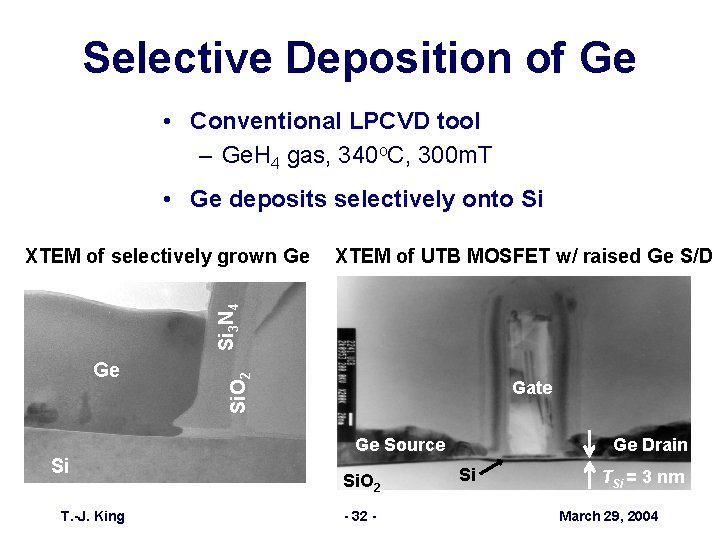
Selective Deposition of Ge • Conventional LPCVD tool – Ge. H 4 gas, 340 o. C, 300 m. T • Ge deposits selectively onto Si XTEM of UTB MOSFET w/ raised Ge S/D Ge Si T. -J. King Si. O 2 Si 3 N 4 XTEM of selectively grown Ge Gate Ge Source Si. O 2 - 32 - Ge Drain Si TSi = 3 nm March 29, 2004

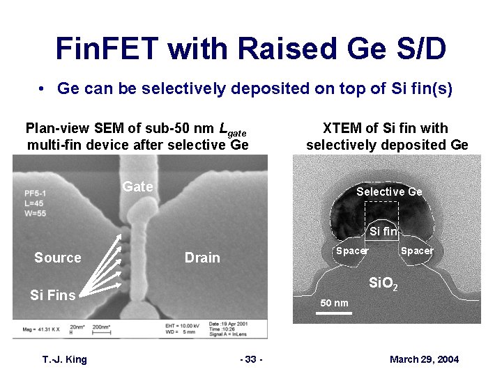
Fin. FET with Raised Ge S/D • Ge can be selectively deposited on top of Si fin(s) Plan-view SEM of sub-50 nm Lgate multi-fin device after selective Ge XTEM of Si fin with selectively deposited Ge Gate Selective Ge Si fin Source Si. O 2 Si Fins T. -J. King Spacer Drain 50 nm - 33 - March 29, 2004

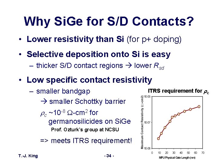
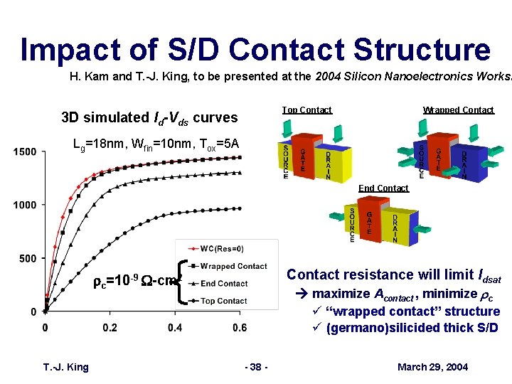
Why Si. Ge for S/D Contacts? • Lower resistivity than Si (for p+ doping) • Selective deposition onto Si is easy – thicker S/D contact regions lower Rsd • Low specific contact resistivity – smaller bandgap smaller Schottky barrier rc ~10 -8 W-cm 2 for germanosilicides on Si. Ge ITRS requirement for rc Prof. Ozturk’s group at NCSU => meets ITRS requirement! T. -J. King - 34 - March 29, 2004

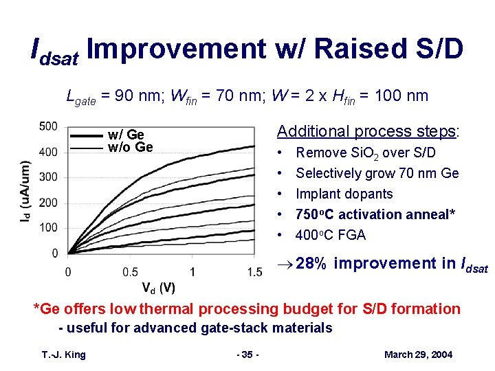
Idsat Improvement w/ Raised S/D Lgate = 90 nm; Wfin = 70 nm; W = 2 x Hfin = 100 nm Additional process steps: w/ Ge w/o Ge • • • Remove Si. O 2 over S/D Selectively grow 70 nm Ge Implant dopants 750 o. C activation anneal* 400 o. C FGA ® 28% improvement in Idsat *Ge offers low thermal processing budget for S/D formation - useful for advanced gate-stack materials T. -J. King - 35 - March 29, 2004

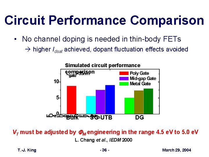
Circuit Performance Comparison • No channel doping is needed in thin-body FETs higher Idsat achieved, dopant fluctuation effects avoided Simulated circuit performance comparison Bulk SG-UTB DG VT must be adjusted by FM engineering in the range 4. 5 e. V to 5. 0 e. V L. Chang et al. , IEDM 2000 T. -J. King - 36 - March 29, 2004

Molybdenum-Gated Fin. FETs Y. -K. Choi et al. , 2002 IEDM N+ Poly. Si Mo S Lg=80 nm, TSi=10 nm Vds=0. 05 V N+ VT shift D W Tbody Lgate • Tilted N implantation (60 ) used for sidewall gates ü N implantation lowers gate work function T. -J. King - 37 - March 29, 2004

Impact of S/D Contact Structure H. Kam and T. -J. King, to be presented at the 2004 Silicon Nanoelectronics Worksh Top Contact 3 D simulated Id-Vds curves Wrapped Contact Lg=18 nm, Wfin=10 nm, Tox=5 A End Contact resistance will limit Idsat maximize Acontact , minimize rc rc=10 -9 W-cm 2 ü “wrapped contact” structure ü (germano)silicided thick S/D T. -J. King - 38 - March 29, 2004

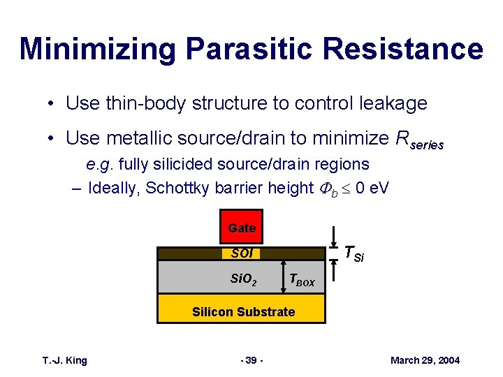
Minimizing Parasitic Resistance • Use thin-body structure to control leakage • Use metallic source/drain to minimize Rseries e. g. fully silicided source/drain regions – Ideally, Schottky barrier height Fb 0 e. V Gate TSi SOI Si. O 2 TBOX Silicon Substrate T. -J. King - 39 - March 29, 2004

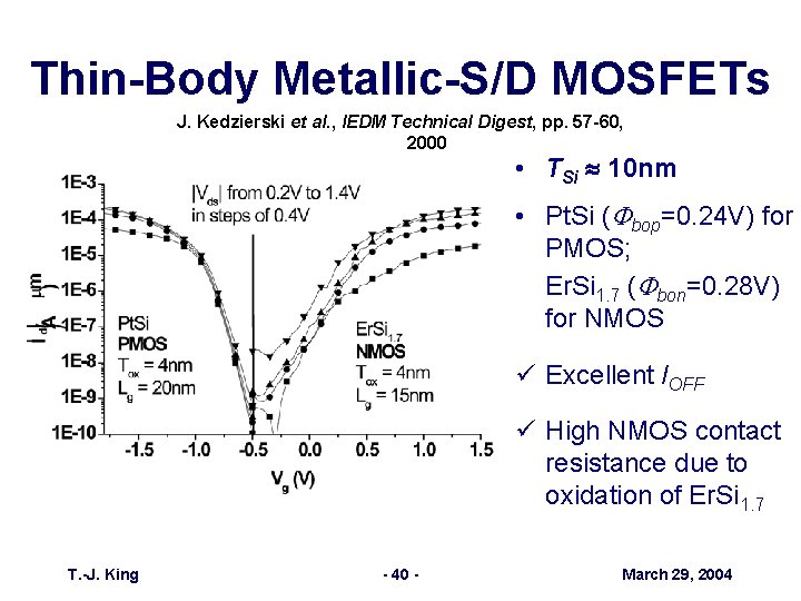
Thin-Body Metallic-S/D MOSFETs J. Kedzierski et al. , IEDM Technical Digest, pp. 57 -60, 2000 • TSi 10 nm • Pt. Si (Fbop=0. 24 V) for PMOS; Er. Si 1. 7 (Fbon=0. 28 V) for NMOS ü Excellent IOFF ü High NMOS contact resistance due to oxidation of Er. Si 1. 7 T. -J. King - 40 - March 29, 2004

Outline • Introduction • Advanced Gate-Stack Materials • Thin-Body MOSFETs • Summary T. -J. King - 41 - March 29, 2004

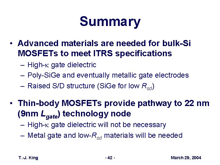
Summary • Advanced materials are needed for bulk-Si MOSFETs to meet ITRS specifications – High-k gate dielectric – Poly-Si. Ge and eventually metallic gate electrodes – Raised S/D structure (Si. Ge for low Rsd) • Thin-body MOSFETs provide pathway to 22 nm (9 nm Lgate) technology node – High-k gate dielectric will not be necessary – Metal gate and low-Rsd materials will be needed T. -J. King - 42 - March 29, 2004

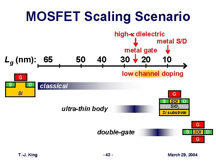
MOSFET Scaling Scenario high-k dielectric metal S/D metal gate Lg (nm): 65 50 40 20 10 low channel doping G S 30 D classical Si G S ultra-thin body SOI D Si. O 2 Si substrate G double-gate S SOI G T. -J. King - 43 - March 29, 2004 D