Advanced Drift Diffusion Device Simulator for 6 H

- Slides: 12

Advanced Drift Diffusion Device Simulator for 6 H and 4 H-Si. C MOSFETs

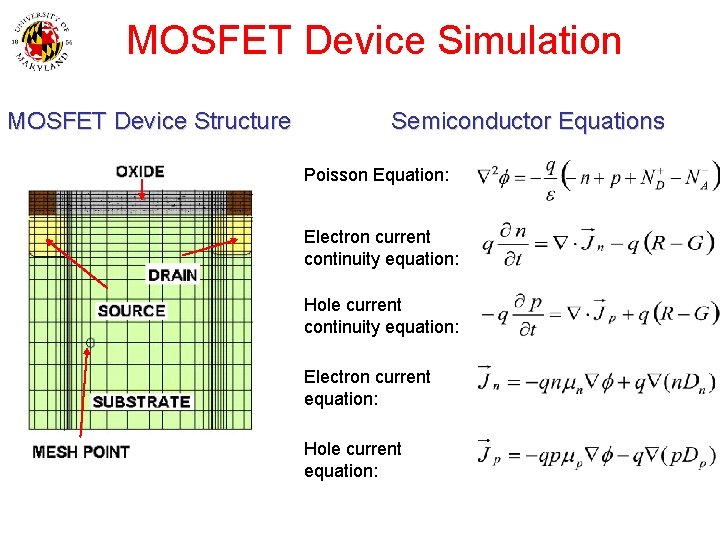
MOSFET Device Simulation MOSFET Device Structure Semiconductor Equations Poisson Equation: Electron current continuity equation: Hole current continuity equation: Electron current equation: Hole current equation:

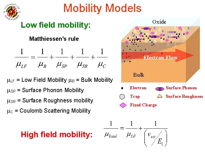
Mobility Models Oxide Low field mobility: Matthiessen's rule Electron Flow m. LF = Low Field Mobility m. B = Bulk Mobility m. SP = Surface Phonon Mobility m. SR = Surface Roughness mobility m. C = Coulomb Scattering Mobility High Field Mobility: High field mobility: Bulk Electron Surface Phonon Trap Surface Roughness Fixed Charge

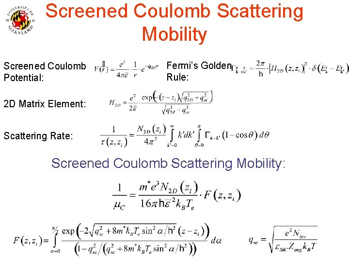
Screened Coulomb Scattering Mobility Screened Coulomb Potential: Fermi’s Golden Rule: 2 D Matrix Element: Scattering Rate: Screened Coulomb Scattering Mobility:

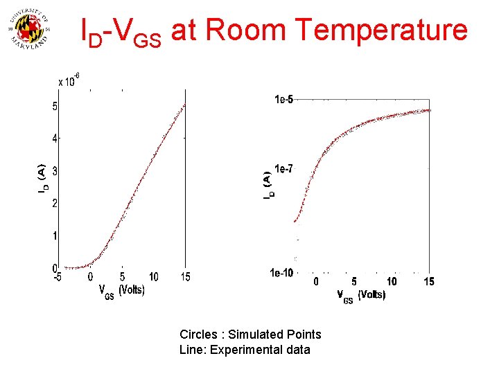
ID-VGS at Room Temperature Circles : Simulated Points Line: Experimental data

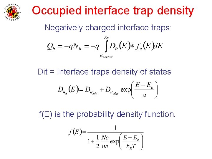
Occupied interface trap density Negatively charged interface traps: Dit = Interface traps density of states f(E) is the probability density function.

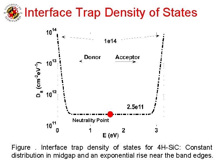
Interface Trap Density of States Neutrality Point Figure. Interface trap density of states for 4 H-Si. C: Constant distribution in midgap and an exponential rise near the band edges.

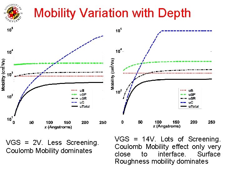
Mobility Variation with Depth VGS = 2 V. Less Screening. Coulomb Mobility dominates VGS = 14 V. Lots of Screening. Coulomb Mobility effect only very close to interface. Surface Roughness mobility dominates

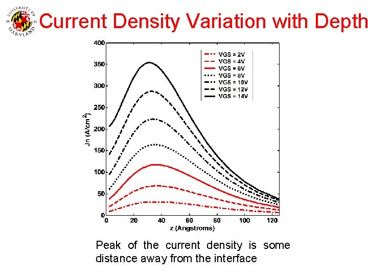
Current Density Variation with Depth Peak of the current density is some distance away from the interface

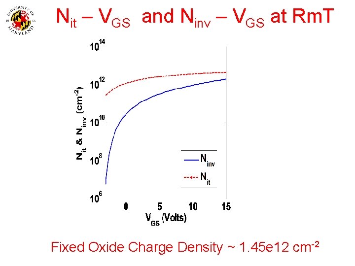
Nit – VGS and Ninv – VGS at Rm. T Fixed Oxide Charge Density ~ 1. 45 e 12 cm-2

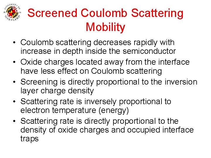
Screened Coulomb Scattering Mobility • Coulomb scattering decreases rapidly with increase in depth inside the semiconductor • Oxide charges located away from the interface have less effect on Coulomb scattering • Screening is directly proportional to the inversion layer charge density • Scattering rate is inversely proportional to electron temperature (energy) • Scattering rate is directly proportional to the density of oxide charges and occupied interface traps

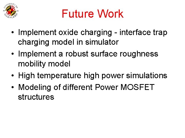
Future Work • Implement oxide charging - interface trap charging model in simulator • Implement a robust surface roughness mobility model • High temperature high power simulations • Modeling of different Power MOSFET structures