Advanced Digital Design with the Verilog HDL Chapter

![Building Blocks for Logic Design v Multiplexers Address[m-1: 0] Data_Out = Data_In[ Address[k] ] Building Blocks for Logic Design v Multiplexers Address[m-1: 0] Data_Out = Data_In[ Address[k] ]](https://slidetodoc.com/presentation_image_h2/067a9074754b04be4daee3deb1113a7e/image-12.jpg)
![Building Blocks for Logic Design v Demultiplexers Address[m-1: 0] Data_Out[n-1: 0] = Data_In[Address[k], k Building Blocks for Logic Design v Demultiplexers Address[m-1: 0] Data_Out[n-1: 0] = Data_In[Address[k], k](https://slidetodoc.com/presentation_image_h2/067a9074754b04be4daee3deb1113a7e/image-13.jpg)

![Vectors in Verilog / Structural Connectivity v sum[3: 0] represent 4 -bits from sum Vectors in Verilog / Structural Connectivity v sum[3: 0] represent 4 -bits from sum](https://slidetodoc.com/presentation_image_h2/067a9074754b04be4daee3deb1113a7e/image-32.jpg)

- Slides: 50

Advanced Digital Design with the Verilog HDL Chapter 1 ~ 5 Verilog 강의자료 REAL TIME ARCHITECTURE LAB

Contents 1. Introduction to Digital Design Methodology 2. Review of Combinational Logic Design 3. Fundamentals of Sequential Logic Design 4. Introduction to Logic Design with Verilog 5. Logic Design with Behavioral Models of Combinational and Sequential Logic Verilog 강의자료 REAL TIME ARCHITECTURE LAB

Introduction to Digital Design Methodology Verilog 강의자료 REAL TIME ARCHITECTURE LAB

CHAPTER 2 Review of Combinational Logic Design Verilog 강의자료 REAL TIME ARCHITECTURE LAB

Review of Combinational Logic Device v Combinational Logic and Boolean Algebra v v Boolean Algebra Theorems for Boolean Algebraic Minimization v Representation of Combinational Logic v v Sum of Products Representation Product of Sums Representation v Simplification of Boolean Expressions v Karnaugh Maps (SOP / POS form) v Glitches and Hazards v Eliminations of Hazards v Building Blocks for Logic Design v v Multiplexers / Demultiplexers Encoder / Decoder Verilog 강의자료 REAL TIME ARCHITECTURE LAB

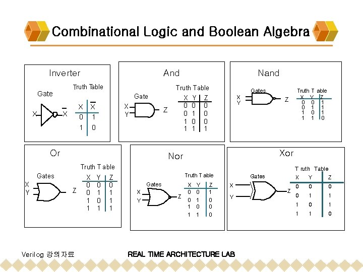
Combinational Logic and Boolean Algebra Inverter Truth Table Gate X And Gate X 0 1 X X 1 0 X Y Z Or Nand Truth Table X Y Z 0 0 1 1 1 Gates X Y Z Xor Nor Truth T able Gates X Y Z Verilog 강의자료 X 0 0 1 1 Y 0 1 Z 0 1 1 1 Truth T able X Y Z 0 0 1 1 1 0 T ruth Table Truth T able Gates X Y Z X 0 0 1 1 Y 0 1 Z 1 0 0 0 Gates X Y REAL TIME ARCHITECTURE LAB Z X Y Z 0 0 1 1 1 0

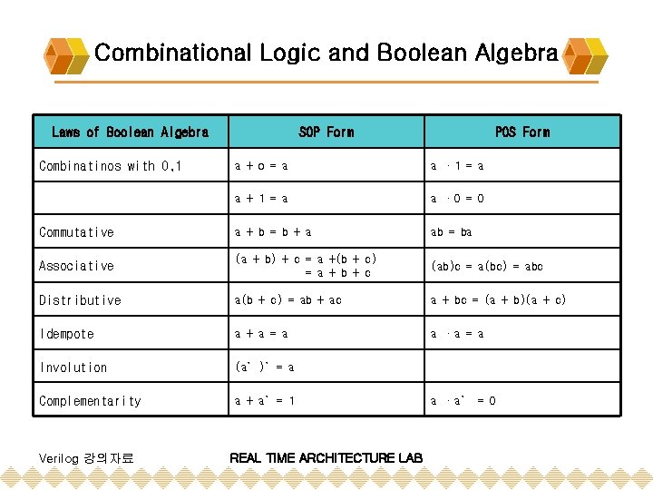
Combinational Logic and Boolean Algebra Laws of Boolean Algebra Combinatinos with 0, 1 SOP Form POS Form a + o = a a · 1 = a a + 1 = a a · 0 = 0 Commutative a + b = b + a ab = ba Associative (a + b) + c = a +(b + c) = a + b + c (ab)c = a(bc) = abc Distributive a(b + c) = ab + ac a + bc = (a + b)(a + c) Idempote a + a = a a ·a = a Involution (a’)’= a Complementarity a + a’= 1 Verilog 강의자료 REAL TIME ARCHITECTURE LAB a ·a’ = 0

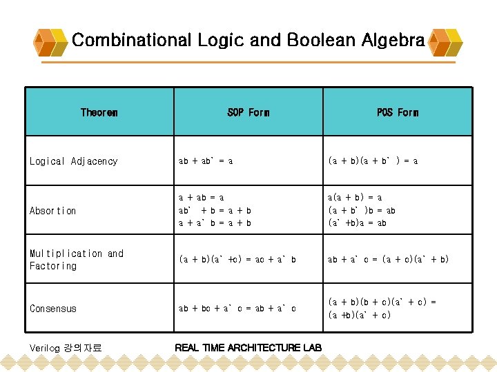
Combinational Logic and Boolean Algebra Theorem SOP Form POS Form Logical Adjacency ab + ab’= a (a + b)(a + b’) = a Absortion a + ab = a ab’ + b = a + b a + a’b = a + b a(a + b) = a (a + b’)b = ab (a’+b)a = ab Multiplication and Factoring (a + b)(a’+c) = ac + a’b ab + a’c = (a + c)(a’+ b) Consensus ab + bc + a’c = ab + a’c (a + b)(b + c)(a’+ c) = (a +b)(a’+ c) Verilog 강의자료 REAL TIME ARCHITECTURE LAB

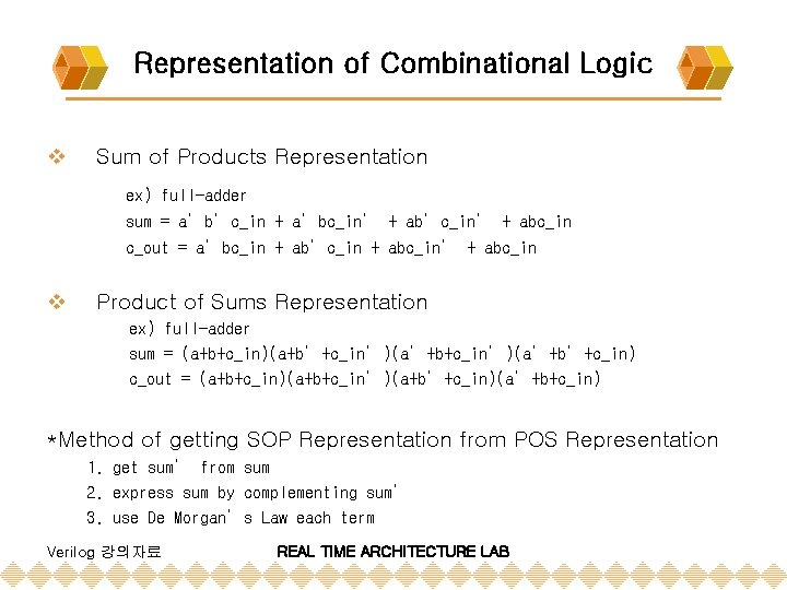
Representation of Combinational Logic v Sum of Products Representation ex) full-adder sum = a’b’c_in + a’bc_in’ + ab’c_in’ + abc_in c_out = a’bc_in + ab’c_in + abc_in’ + abc_in v Product of Sums Representation ex) full-adder sum = (a+b+c_in)(a+b’+c_in’)(a’+b’+c_in) c_out = (a+b+c_in)(a+b+c_in’)(a+b’+c_in)(a’+b+c_in) *Method of getting SOP Representation from POS Representation 1. get sum’ from sum 2. express sum by complementing sum’ 3. use De Morgan’s Law each term Verilog 강의자료 REAL TIME ARCHITECTURE LAB

Simplification of Boolean Expressions v SOP : 2 -level AND, OR logic circuit. v K-map ( SOP ) v use value-1 and don’t care v K-map ( POS ) v v use value-0 and don’t care use De Morgan’s Law v K-map ( Don’t care ) v fast by using don’t care Verilog 강의자료 REAL TIME ARCHITECTURE LAB

Glitches and Hazards v Glitches v delays of actual implementation and circuit structure v Hazards v glitch caused by input signal v Static Hazards v v 0 -hazard , 1 -hazard caused by differential propagation delays ( Figure 2 -32, 33 ) v Eliminate Static Hazards v use k-map and check Redundant cube ( Figure 2 -34 ) v Dynamic Hazards v caused by many static-hazard v Eliminate Dynamic Hazards v v transform circuit into a two-level form detect and eliminate all static hazards Verilog 강의자료 REAL TIME ARCHITECTURE LAB
![Building Blocks for Logic Design v Multiplexers Addressm1 0 DataOut DataIn Addressk Building Blocks for Logic Design v Multiplexers Address[m-1: 0] Data_Out = Data_In[ Address[k] ]](https://slidetodoc.com/presentation_image_h2/067a9074754b04be4daee3deb1113a7e/image-12.jpg)
Building Blocks for Logic Design v Multiplexers Address[m-1: 0] Data_Out = Data_In[ Address[k] ] Data_In[n-1] Data_Out Data_In[0] Verilog 강의자료 REAL TIME ARCHITECTURE LAB
![Building Blocks for Logic Design v Demultiplexers Addressm1 0 DataOutn1 0 DataInAddressk k Building Blocks for Logic Design v Demultiplexers Address[m-1: 0] Data_Out[n-1: 0] = Data_In[Address[k], k](https://slidetodoc.com/presentation_image_h2/067a9074754b04be4daee3deb1113a7e/image-13.jpg)
Building Blocks for Logic Design v Demultiplexers Address[m-1: 0] Data_Out[n-1: 0] = Data_In[Address[k], k = 0: m-1 ] Data_Out[n-1] Data_In Data_Out[0] Verilog 강의자료 REAL TIME ARCHITECTURE LAB

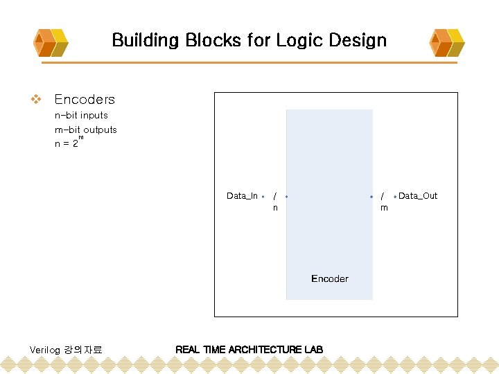
Building Blocks for Logic Design v Encoders n-bit inputs m-bit outputs m n=2 Data_In Verilog 강의자료 / n REAL TIME ARCHITECTURE LAB / m Data_Out

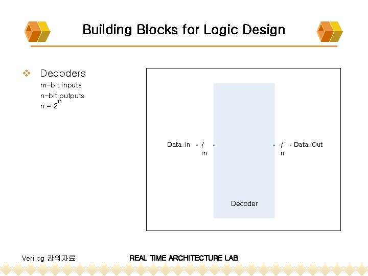
Building Blocks for Logic Design v Decoders m-bit inputs n-bit outputs m n=2 Data_In Verilog 강의자료 / m REAL TIME ARCHITECTURE LAB / n Data_Out

CHAPTER 3 Fundamentals of Sequential Logic Device Verilog 강의자료 REAL TIME ARCHITECTURE LAB

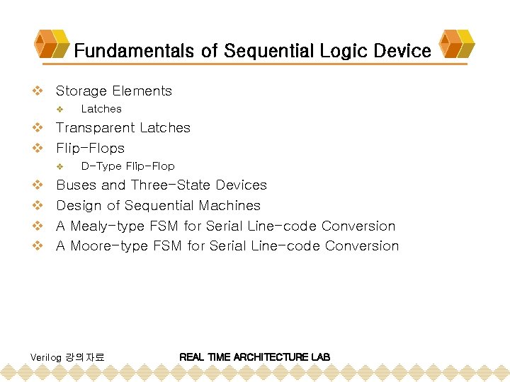
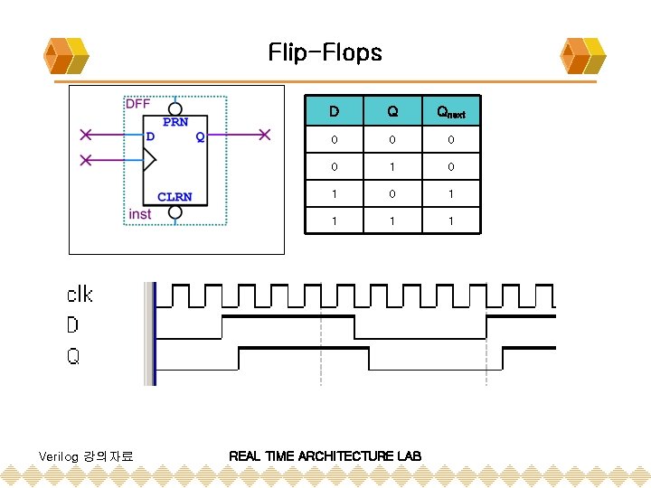
Fundamentals of Sequential Logic Device v Storage Elements v Latches v Transparent Latches v Flip-Flops v v v D-Type Flip-Flop Buses and Three-State Devices Design of Sequential Machines A Mealy-type FSM for Serial Line-code Conversion A Moore-type FSM for Serial Line-code Conversion Verilog 강의자료 REAL TIME ARCHITECTURE LAB

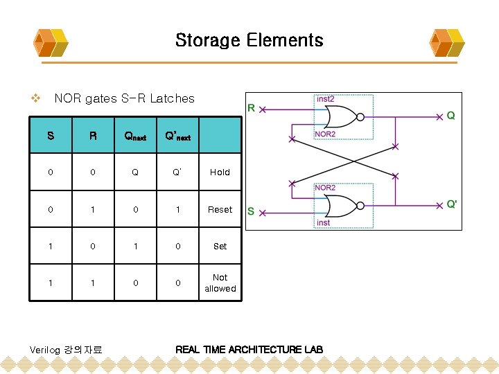
Storage Elements v NOR gates S-R Latches S R Qnext Q’next 0 0 Q Q’ Hold 0 1 Reset 1 0 Set 1 1 0 0 Not allowed Verilog 강의자료 REAL TIME ARCHITECTURE LAB

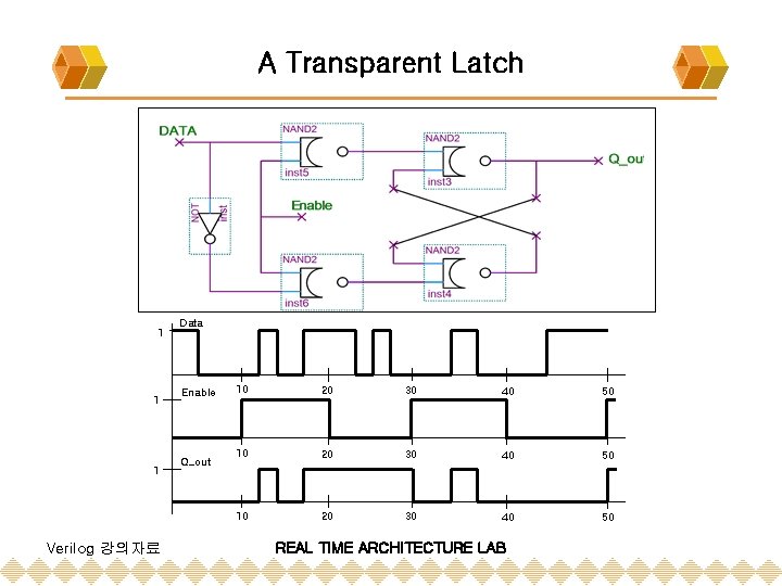
A Transparent Latch 1 1 1 Verilog 강의자료 Data Enable Q_out 10 20 30 40 50 REAL TIME ARCHITECTURE LAB

Flip-Flops Verilog 강의자료 D Q Qnext 0 0 1 0 1 1 REAL TIME ARCHITECTURE LAB

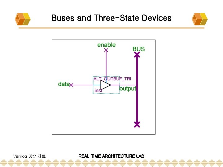
Buses and Three-State Devices Verilog 강의자료 REAL TIME ARCHITECTURE LAB

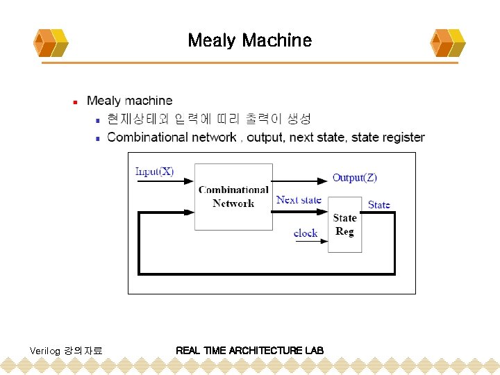
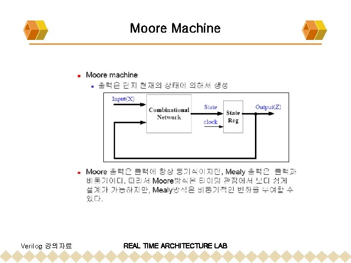
Design of Sequential Machines v Edge-triggered v v rising-edge falling-edge v State Machine v v Finite State Machine ( FSM ) : always finite number of states : n-bits word state => 2 n states v Mealy Machine v outputs and the next state depend on the present state + inputs v Moore Machine v outputs depends on the present state Verilog 강의자료 REAL TIME ARCHITECTURE LAB

Mealy Machine Verilog 강의자료 REAL TIME ARCHITECTURE LAB

Moore Machine Verilog 강의자료 REAL TIME ARCHITECTURE LAB

CHAPTER 4 Introduction to Logic Design with Verilog 강의자료 REAL TIME ARCHITECTURE LAB

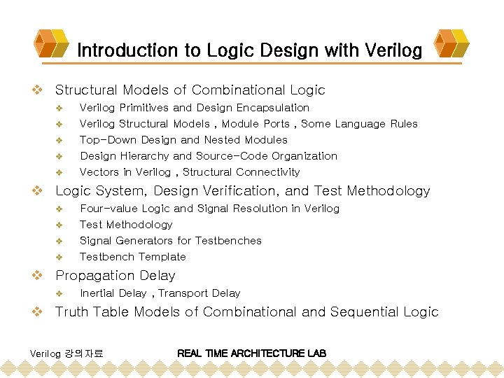
Introduction to Logic Design with Verilog v Structural Models of Combinational Logic v v v Verilog Primitives and Design Encapsulation Verilog Structural Models , Module Ports , Some Language Rules Top-Down Design and Nested Modules Design Hierarchy and Source-Code Organization Vectors in Verilog , Structural Connectivity v Logic System, Design Verification, and Test Methodology v v Four-value Logic and Signal Resolution in Verilog Test Methodology Signal Generators for Testbenches Testbench Template v Propagation Delay v Inertial Delay , Transport Delay v Truth Table Models of Combinational and Sequential Logic Verilog 강의자료 REAL TIME ARCHITECTURE LAB

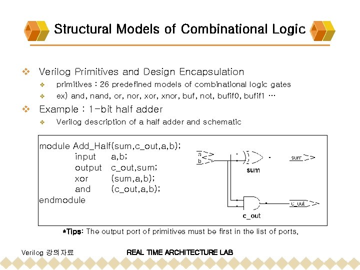
Structural Models of Combinational Logic v Verilog Primitives and Design Encapsulation v v primitives : 26 predefined models of combinational logic gates ex) and, nand, or, nor, xnor, buf, not, bufif 0, bufif 1 … v Example : 1 -bit half adder v Verilog description of a half adder and schematic module Add_Half(sum, c_out, a, b); input a, b; output c_out, sum; xor (sum, a, b); and (c_out, a, b); endmodule *Tips: The output port of primitives must be first in the list of ports. Verilog 강의자료 REAL TIME ARCHITECTURE LAB

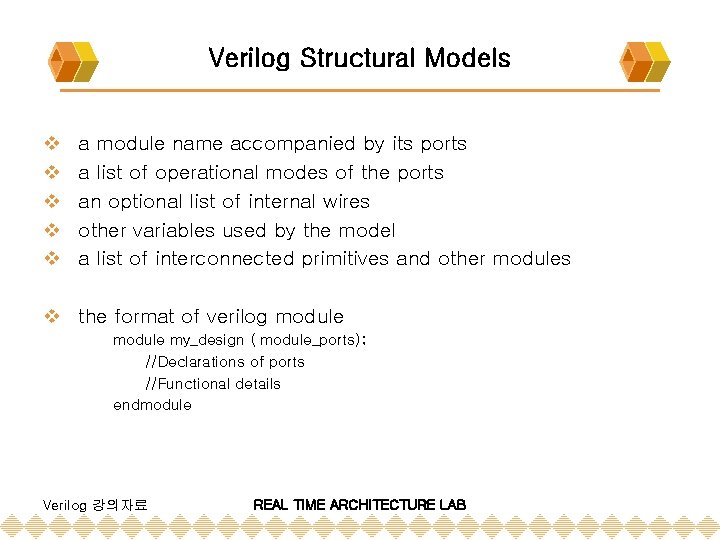
Verilog Structural Models v v v a module name accompanied by its ports a list of operational modes of the ports an optional list of internal wires other variables used by the model a list of interconnected primitives and other modules v the format of verilog module my_design ( module_ports); //Declarations of ports //Functional details endmodule Verilog 강의자료 REAL TIME ARCHITECTURE LAB

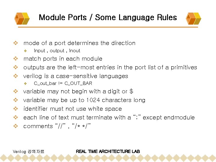
Module Ports / Some Language Rules v mode of a port determines the direction v input , output , inout v match ports in each module v outputs are the left-most entries in the port list of a primitives v verilog is a case-sensitive languages v v v C_out_bar != C_OUT_BAR variable may not begin with a digit or $ variable may be up to 1024 characters long identifier must not use white space each line of text must terminate with a “; ” except endmodule comments “//” , “/* */” Verilog 강의자료 REAL TIME ARCHITECTURE LAB

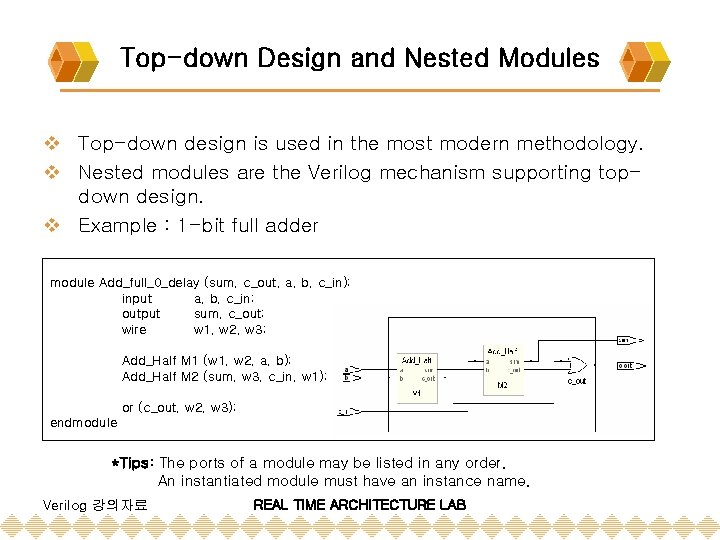
Top-down Design and Nested Modules v Top-down design is used in the most modern methodology. v Nested modules are the Verilog mechanism supporting topdown design. v Example : 1 -bit full adder module Add_full_0_delay (sum, c_out, a, b, c_in); input a, b, c_in; output sum, c_out; wire w 1, w 2, w 3; Add_Half M 1 (w 1, w 2, a, b); Add_Half M 2 (sum, w 3, c_in, w 1); or (c_out, w 2, w 3); endmodule *Tips: The ports of a module may be listed in any order. An instantiated module must have an instance name. Verilog 강의자료 REAL TIME ARCHITECTURE LAB

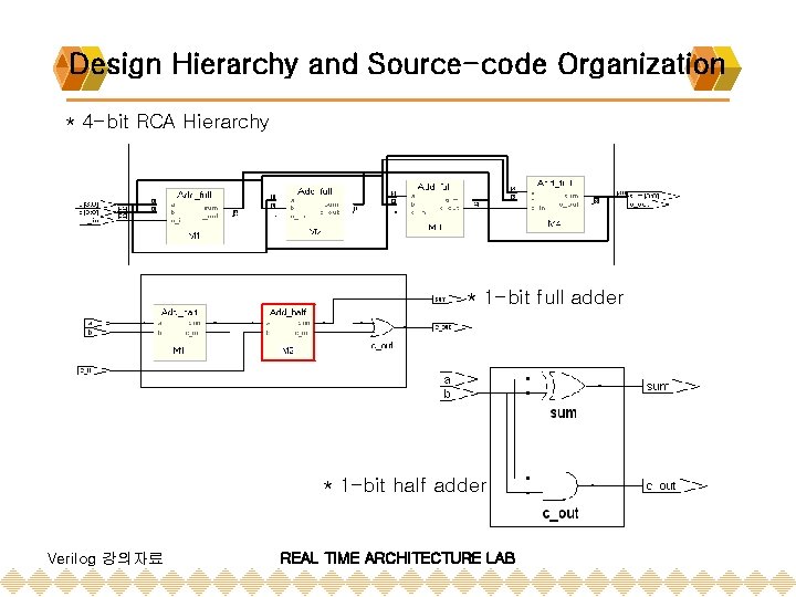
Design Hierarchy and Source-code Organization * 4 -bit RCA Hierarchy * 1 -bit full adder * 1 -bit half adder Verilog 강의자료 REAL TIME ARCHITECTURE LAB
![Vectors in Verilog Structural Connectivity v sum3 0 represent 4 bits from sum Vectors in Verilog / Structural Connectivity v sum[3: 0] represent 4 -bits from sum](https://slidetodoc.com/presentation_image_h2/067a9074754b04be4daee3deb1113a7e/image-32.jpg)
Vectors in Verilog / Structural Connectivity v sum[3: 0] represent 4 -bits from sum v decimal 4 = 0100 binary, sum[2] = 1 v Use nets to establish structural connectivity. v An undeclared identifier is treated by default as a wire v Example : Formal and actual names for port association … Add_half_0_delay M 1 (. b(b), . c_out(w 2), . a(a), sum(w 1) ); Add_half_0_delay M 1 (w 1, w 2, a, b); … module Add_half_0_delay (sum, c_out, a, b); Verilog 강의자료 REAL TIME ARCHITECTURE LAB

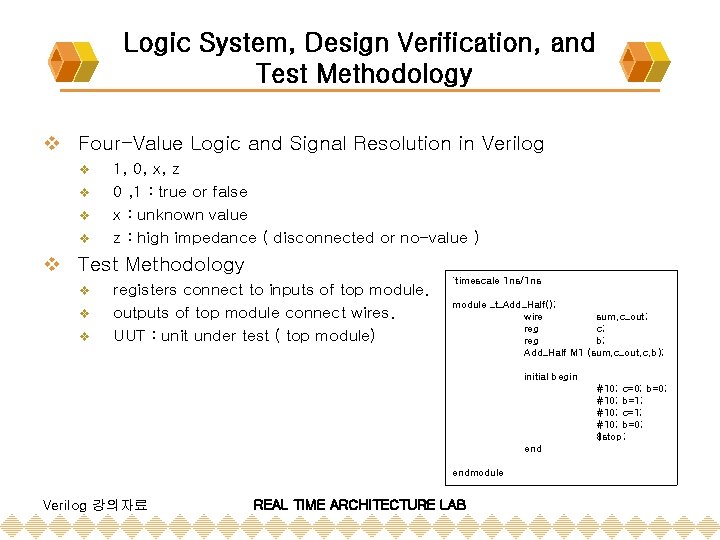
Logic System, Design Verification, and Test Methodology v Four-Value Logic and Signal Resolution in Verilog v v 1, 0, x, z 0 , 1 : true or false x : unknown value z : high impedance ( disconnected or no-value ) v Test Methodology v v v registers connect to inputs of top module. outputs of top module connect wires. UUT : unit under test ( top module) `timescale 1 ns/1 ns module _t_Add_Half(); wire sum, c_out; reg c; reg b; Add_Half M 1 (sum, c_out, c, b); initial begin #10; c=0; b=0; #10; b=1; #10; c=1; #10; b=0; $stop; endmodule Verilog 강의자료 REAL TIME ARCHITECTURE LAB

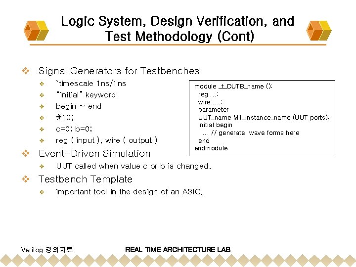
Logic System, Design Verification, and Test Methodology (Cont) v Signal Generators for Testbenches v v v `timescale 1 ns/1 ns “initial” keyword begin ~ end #10; c=0; b=0; reg ( input ), wire ( output ) v Event-Driven Simulation v module _t_DUTB_name (); reg. . . ; wire. . ; parameter UUT_name M 1_instance_name (UUT ports); initial begin. . . // generate wave forms here endmodule UUT called when value c or b is changed. v Testbench Template v important tool in the design of an ASIC. Verilog 강의자료 REAL TIME ARCHITECTURE LAB

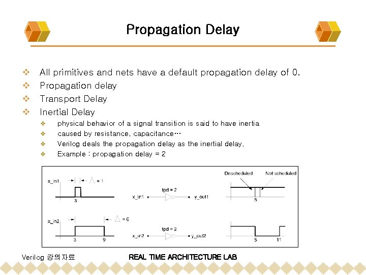
Propagation Delay v v All primitives and nets have a default propagation delay of 0. Propagation delay Transport Delay Inertial Delay v v physical behavior of a signal transition is said to have inertia caused by resistance, capacitance… Verilog deals the propagation delay as the inertial delay. Example : propagation delay = 2 Verilog 강의자료 REAL TIME ARCHITECTURE LAB

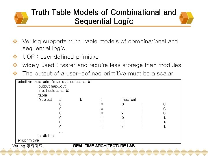
Truth Table Models of Combinational and Sequential Logic v Verilog supports truth-table models of combinational and sequential logic. v UDP : user defined primitive v widely used : faster and require less storage than modules. v The output of a user-defined primitive must be a scalar. primitive mux_prim (mux_out, select, a, b) output mux_out; input select, a, b; table //select a b 0 0 0. . . endtable endprimitive Verilog 강의자료 : 0 0 0 1 1 1 mux_out 0 1 x REAL TIME ARCHITECTURE LAB : : : 0; 0; 0; 1; 1; 1;

CHAPTER 5 Logic Design with Behavioral Models of Combinational and Sequential logic Verilog 강의자료 REAL TIME ARCHITECTURE LAB

Logic Design with Behavioral Models of Combinational and Sequential logic v v v v Behavioral Modeling Propagation Delay and Continuous Assignments Cyclic Behavioral Models of Flip-Flops and Latches Cyclic Behavior and Edge Detection Behavioral Models of Multiplexers, Encoders, and Decoders Algorithmic State Machine Charts for Behavioral Modeling ASMD Charts Shift Register Verilog 강의자료 REAL TIME ARCHITECTURE LAB

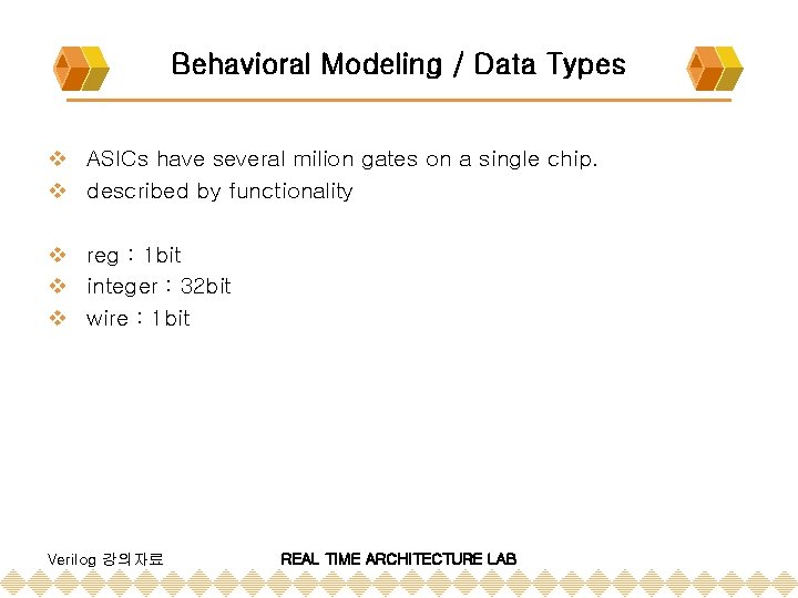
Behavioral Modeling / Data Types v ASICs have several milion gates on a single chip. v described by functionality v reg : 1 bit v integer : 32 bit v wire : 1 bit Verilog 강의자료 REAL TIME ARCHITECTURE LAB

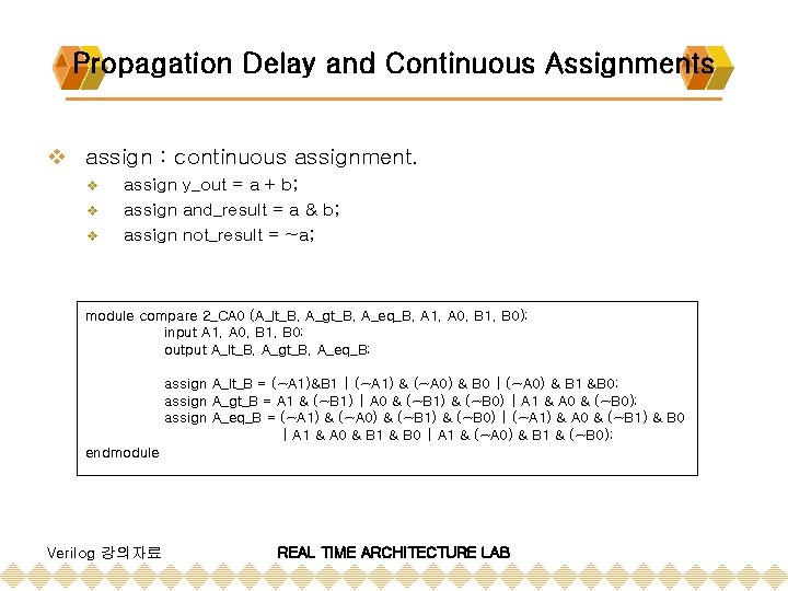
Propagation Delay and Continuous Assignments v assign : continuous assignment. v v v assign y_out = a + b; assign and_result = a & b; assign not_result = ~a; module compare 2_CA 0 (A_lt_B, A_gt_B, A_eq_B, A 1, A 0, B 1, B 0); input A 1, A 0, B 1, B 0; output A_lt_B, A_gt_B, A_eq_B; assign A_lt_B = (~A 1)&B 1 | (~A 1) & (~A 0) & B 0 | (~A 0) & B 1 &B 0; assign A_gt_B = A 1 & (~B 1) | A 0 & (~B 1) & (~B 0) | A 1 & A 0 & (~B 0); assign A_eq_B = (~A 1) & (~A 0) & (~B 1) & (~B 0) | (~A 1) & A 0 & (~B 1) & B 0 | A 1 & A 0 & B 1 & B 0 | A 1 & (~A 0) & B 1 & (~B 0); endmodule Verilog 강의자료 REAL TIME ARCHITECTURE LAB

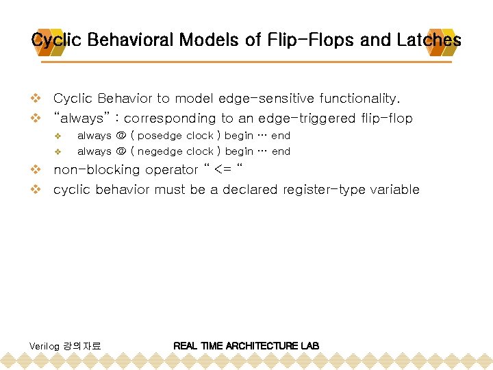
Cyclic Behavioral Models of Flip-Flops and Latches v Cyclic Behavior to model edge-sensitive functionality. v “always” : corresponding to an edge-triggered flip-flop v v always @ ( posedge clock ) begin … end always @ ( negedge clock ) begin … end v non-blocking operator “ <= “ v cyclic behavior must be a declared register-type variable Verilog 강의자료 REAL TIME ARCHITECTURE LAB

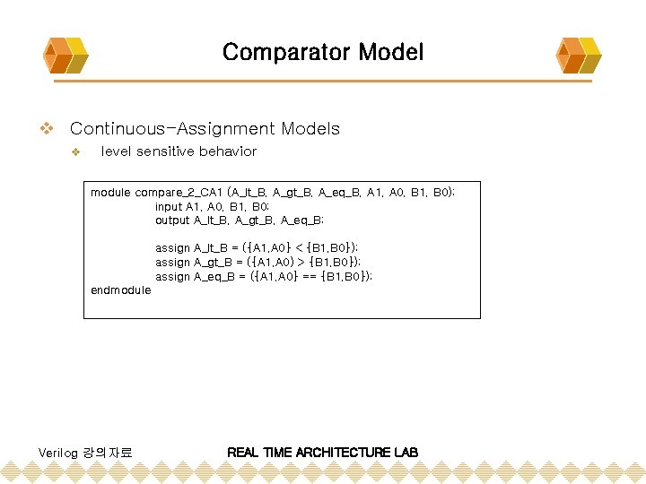
Comparator Model v Continuous-Assignment Models v level sensitive behavior module compare_2_CA 1 (A_lt_B, A_gt_B, A_eq_B, A 1, A 0, B 1, B 0); input A 1, A 0, B 1, B 0; output A_lt_B, A_gt_B, A_eq_B; assign A_lt_B = ({A 1, A 0} < {B 1, B 0}); assign A_gt_B = ({A 1, A 0) > {B 1, B 0}); assign A_eq_B = ({A 1, A 0} == {B 1, B 0}); endmodule Verilog 강의자료 REAL TIME ARCHITECTURE LAB

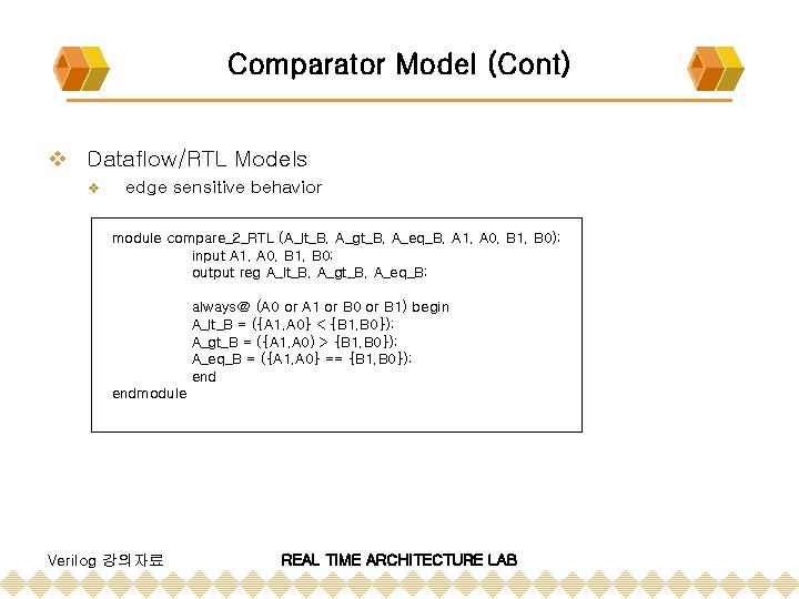
Comparator Model (Cont) v Dataflow/RTL Models v edge sensitive behavior module compare_2_RTL (A_lt_B, A_gt_B, A_eq_B, A 1, A 0, B 1, B 0); input A 1, A 0, B 1, B 0; output reg A_lt_B, A_gt_B, A_eq_B; always@ (A 0 or A 1 or B 0 or B 1) begin A_lt_B = ({A 1, A 0} < {B 1, B 0}); A_gt_B = ({A 1, A 0) > {B 1, B 0}); A_eq_B = ({A 1, A 0} == {B 1, B 0}); endmodule Verilog 강의자료 REAL TIME ARCHITECTURE LAB

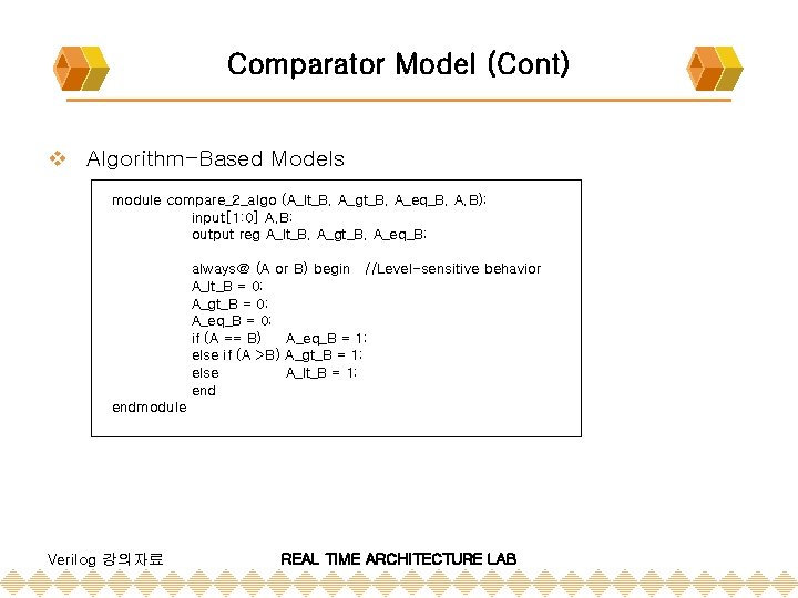
Comparator Model (Cont) v Algorithm-Based Models module compare_2_algo (A_lt_B, A_gt_B, A_eq_B, A, B); input[1: 0] A, B; output reg A_lt_B, A_gt_B, A_eq_B; always@ (A or B) begin //Level-sensitive behavior A_lt_B = 0; A_gt_B = 0; A_eq_B = 0; if (A == B) A_eq_B = 1; else if (A >B) A_gt_B = 1; else A_lt_B = 1; endmodule Verilog 강의자료 REAL TIME ARCHITECTURE LAB

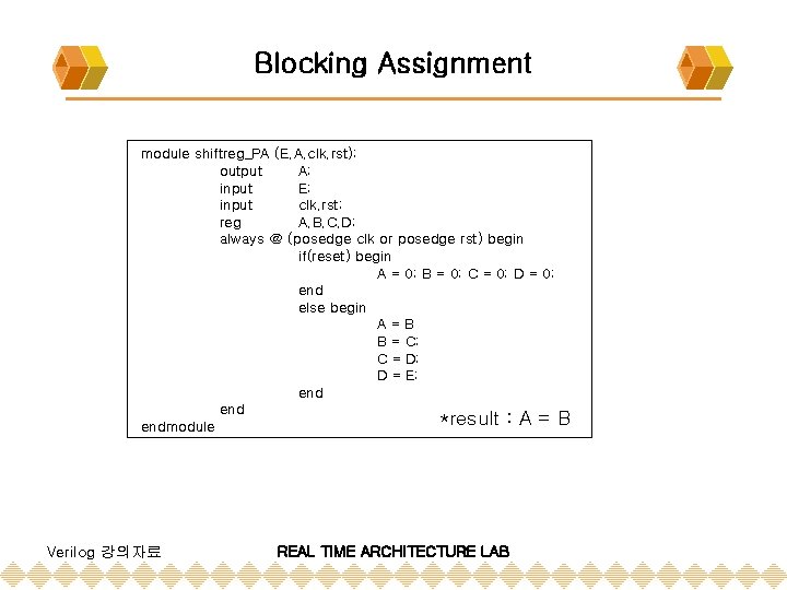
Blocking Assignment module shiftreg_PA (E, A, clk, rst); output A; input E; input clk, rst; reg A, B, C, D; always @ (posedge clk or posedge rst) begin if(reset) begin A = 0; B = 0; C = 0; D = 0; end else begin A=B B = C; C = D; D = E; end *result : A = B endmodule Verilog 강의자료 REAL TIME ARCHITECTURE LAB

Blocking Assignment (Cont) module shiftreg_PA_rev (E, A, clk, rst); output A; input E; input clk, rst; reg A, B, C, D; always @ (posedge clk or posedge rst) begin if(reset) begin A = 0; B = 0; C = 0; D = 0; end else begin D=E C = D; B = C; A = B; end * result : A = E endmodule Verilog 강의자료 REAL TIME ARCHITECTURE LAB

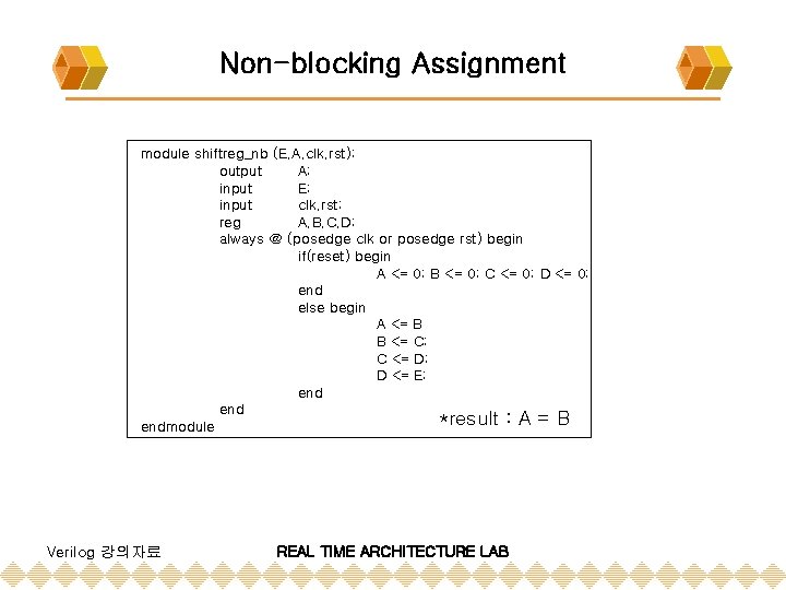
Non-blocking Assignment module shiftreg_nb (E, A, clk, rst); output A; input E; input clk, rst; reg A, B, C, D; always @ (posedge clk or posedge rst) begin if(reset) begin A <= 0; B <= 0; C <= 0; D <= 0; end else begin A <= B B <= C; C <= D; D <= E; end *result : A = B endmodule Verilog 강의자료 REAL TIME ARCHITECTURE LAB

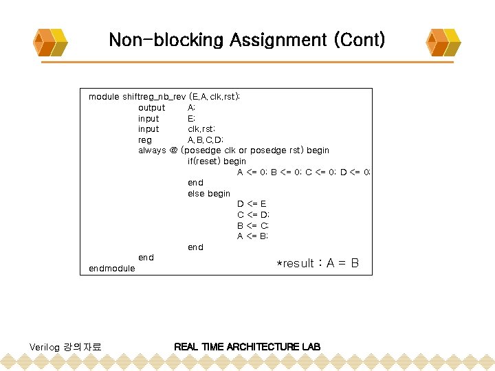
Non-blocking Assignment (Cont) module shiftreg_nb_rev (E, A, clk, rst); output A; input E; input clk, rst; reg A, B, C, D; always @ (posedge clk or posedge rst) begin if(reset) begin A <= 0; B <= 0; C <= 0; D <= 0; end else begin D <= E C <= D; B <= C; A <= B; end *result : A = B endmodule Verilog 강의자료 REAL TIME ARCHITECTURE LAB

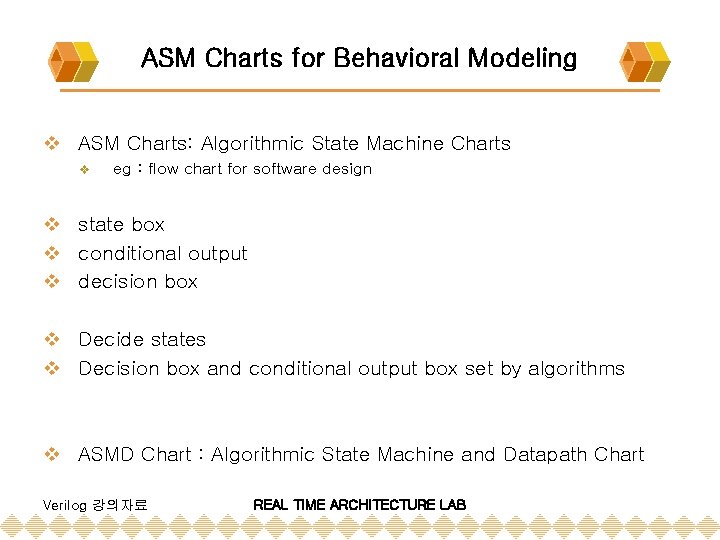
ASM Charts for Behavioral Modeling v ASM Charts: Algorithmic State Machine Charts v eg : flow chart for software design v state box v conditional output v decision box v Decide states v Decision box and conditional output box set by algorithms v ASMD Chart : Algorithmic State Machine and Datapath Chart Verilog 강의자료 REAL TIME ARCHITECTURE LAB

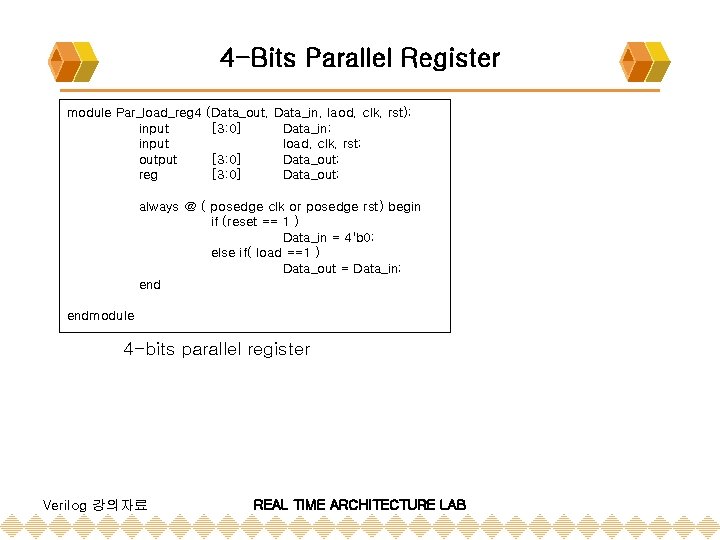
4 -Bits Parallel Register module Par_load_reg 4 input output reg (Data_out, Data_in, laod, clk, rst); [3: 0] Data_in; load, clk, rst; [3: 0] Data_out; always @ ( posedge clk or posedge rst) begin if (reset == 1 ) Data_in = 4'b 0; else if( load ==1 ) Data_out = Data_in; endmodule 4 -bits parallel register Verilog 강의자료 REAL TIME ARCHITECTURE LAB