Advanced CMOS and Interconnect Technologies A Marchioro PHESE
![Costs/Performance[$] Bad news Good news _________________ [$] Normalized to 250 nm generation A. Marchioro Costs/Performance[$] Bad news Good news _________________ [$] Normalized to 250 nm generation A. Marchioro](https://slidetodoc.com/presentation_image/570cd29068c9c8b1bf54b940b50bcfa3/image-16.jpg)
- Slides: 28

Advanced CMOS and Interconnect Technologies A. Marchioro / PH-ESE

Highly non-technical Mildly technical Topics • CMOS – Current state of the art – Obstacles ahead – Perspective solutions and ITRS predictions • Interconnect • More than Moore • Conclusions – What to do A. Marchioro / FCC Meeting Feb-2015

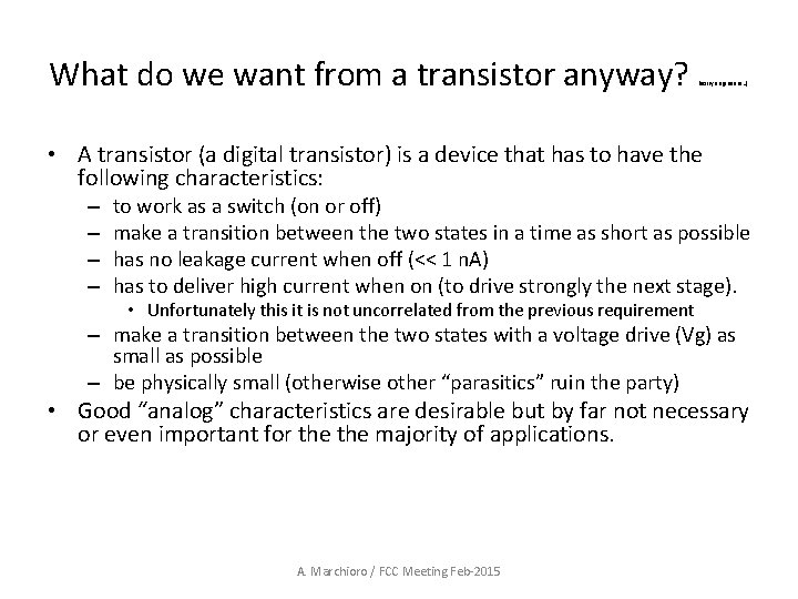
What do we want from a transistor anyway? (sorry engineers…) • A transistor (a digital transistor) is a device that has to have the following characteristics: – – to work as a switch (on or off) make a transition between the two states in a time as short as possible has no leakage current when off (<< 1 n. A) has to deliver high current when on (to drive strongly the next stage). • Unfortunately this it is not uncorrelated from the previous requirement – make a transition between the two states with a voltage drive (Vg) as small as possible – be physically small (otherwise other “parasitics” ruin the party) • Good “analog” characteristics are desirable but by far not necessary or even important for the majority of applications. A. Marchioro / FCC Meeting Feb-2015

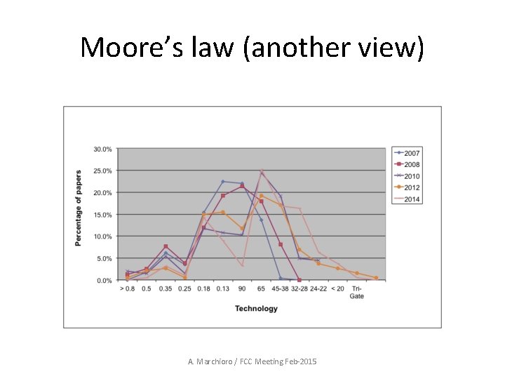
Moore’s law (another view) A. Marchioro / FCC Meeting Feb-2015

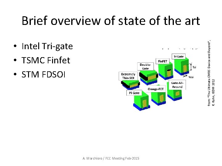
Brief overview of state of the art from: “The Ultimate CMOS Device and Beyond”, K. Kuhn, IEDM 2012 • Intel Tri-gate • TSMC Finfet • STM FDSOI A. Marchioro / FCC Meeting Feb-2015

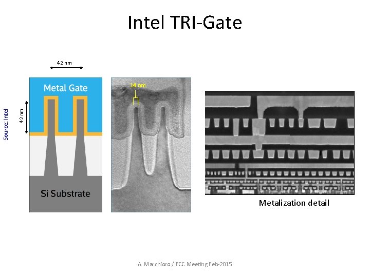
Intel TRI-Gate 42 nm Source: Intel 14 nm Metalization detail A. Marchioro / FCC Meeting Feb-2015

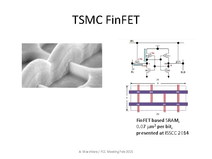
TSMC Fin. FET based SRAM, 0. 07 mm 2 per bit, presented at ISSCC 2014 A. Marchioro / FCC Meeting Feb-2015

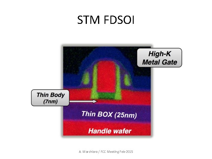
STM FDSOI A. Marchioro / FCC Meeting Feb-2015

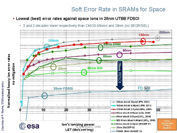
Soft Error Rate in SRAMs for Space Lowest (best) error rates against space ions in 28 nm UTBB FDSOI Normalized heavy ion error rates Arbitrary units no mitigation 28 nm FDSOI Courtesy of P. Roche, STMicroelectronics • 3 and 2 decades lower respectively than CMOS 65 nmn and 28 nm (no SEGR/SEL) Ion’s ionizing power A. Marchioro / CERN Roche, ESA QCA Days 07’ 09’ 11’ 9 NSREC’ 14

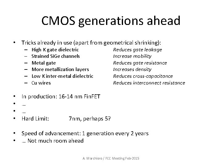
CMOS generations ahead • Tricks already in use (apart from geometrical shrinking): – High K gate dielectric – Strained Si. Ge channels – Metal gate – More metallization layers – Low K inter-metal dielectric – Cu wires • • Reduces gate leakage Increase mobility Reduces gate resistance Increases density Reduces cross-capacitance Reduces interconnect resistance In production: 16 -14 nm Fin. FET … … Hard Limit: 7 nm, perhaps 5? • Speed of advancement: 1 generation every 2 years • … Not much room ahead A. Marchioro / FCC Meeting Feb-2015

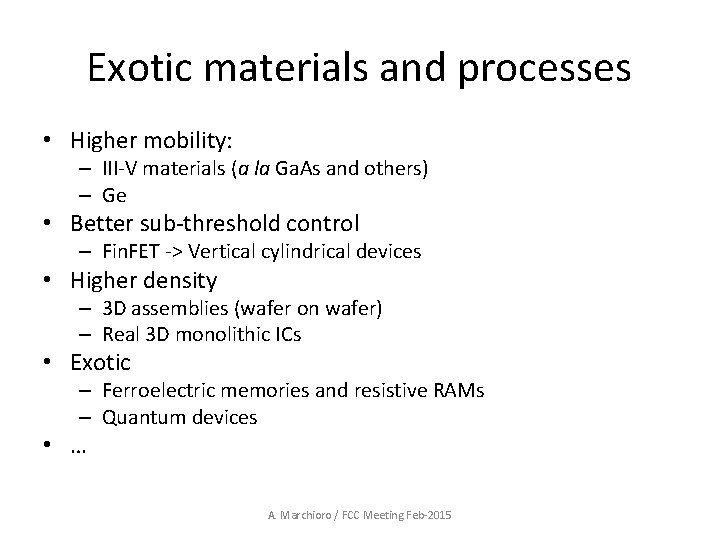
Exotic materials and processes • Higher mobility: – III-V materials (a la Ga. As and others) – Ge • Better sub-threshold control – Fin. FET -> Vertical cylindrical devices • Higher density – 3 D assemblies (wafer on wafer) – Real 3 D monolithic ICs • Exotic – Ferroelectric memories and resistive RAMs – Quantum devices • … A. Marchioro / FCC Meeting Feb-2015

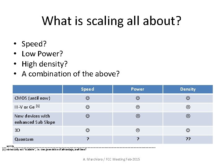
What is scaling all about? • • Speed? Low Power? High density? A combination of the above? Speed Power Density CMOS (until now) III-V or Ge [1] New devices with enhanced Sub Slope 3 D Quantum ? ? ? ? ___NOTES___________________________________________________ [1] Intrinsically not “scalable”, i. e. one generation of advantage, and then? A. Marchioro / FCC Meeting Feb-2015

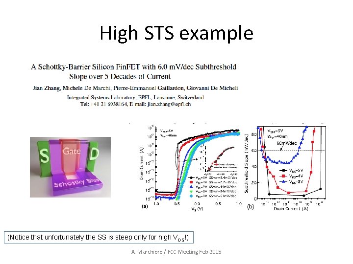
High STS example (Notice that unfortunately the SS is steep only for high VDS!) A. Marchioro / FCC Meeting Feb-2015

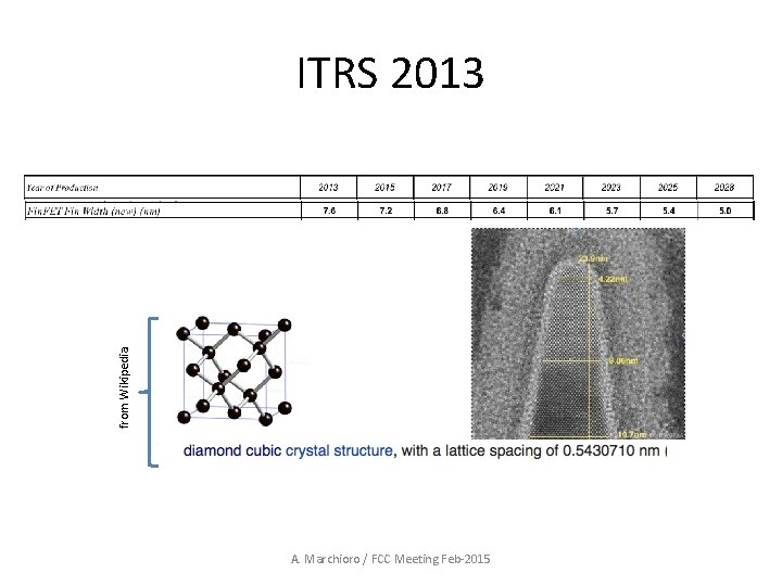
from Wikipedia ITRS 2013 A. Marchioro / FCC Meeting Feb-2015

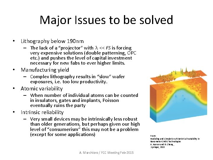
Major Issues to be solved • Lithography below 190 nm – The lack of a “projector” with l << FS is forcing very expensive solutions (double patterning, OPC etc. ) and pushes the level of capital investment necessary for new fabs to ever higher limits. • Manufacturing yield – Complex lithography results in “slow” wafer exposures, i. e. too low productivity. • Atomic variability – When number of individual atoms can be counted in insulators, gates and implants, Poisson eventually ruins the party • Intrinsic reliability – Very small devices may be intrinsically less robust than older generations, but perhaps given our high level of “consumerism” this may not be a problem (except for some applications) A. Marchioro / FCC Meeting Feb-2015 From: Modeling and Simulation of Statistical Variability in Nanometer CMOS Technologies A. Asenov and B. Cheng , Springer, 2011
![CostsPerformance Bad news Good news Normalized to 250 nm generation A Marchioro Costs/Performance[$] Bad news Good news _________________ [$] Normalized to 250 nm generation A. Marchioro](https://slidetodoc.com/presentation_image/570cd29068c9c8b1bf54b940b50bcfa3/image-16.jpg)
Costs/Performance[$] Bad news Good news _________________ [$] Normalized to 250 nm generation A. Marchioro / FCC Meeting Feb-2015

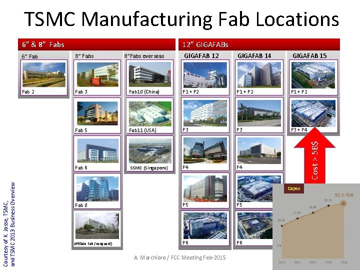
TSMC Manufacturing Fab Locations 12” GIGAFABs Courtesy of K. Josse, TSMC, and TSMC 2013 Business Overview 6” & 8” Fabs GIGAFAB 12 GIGAFAB 14 GIGAFAB 15 8” Fabs Fab 2 Fab 3 Fab 10 (China) P 1 + P 2 Fab 5 Fab 11 (USA) P 3 P 3 + P 4 Fab 6 SSMC (Singapore) P 4 8”Fabs overseas Cost > 5 B$ 6” Fab Capex Fab 8 Affiliate Fab (Vanguard) P 5 P 6 A. Marchioro / FCC Meeting Feb-2015

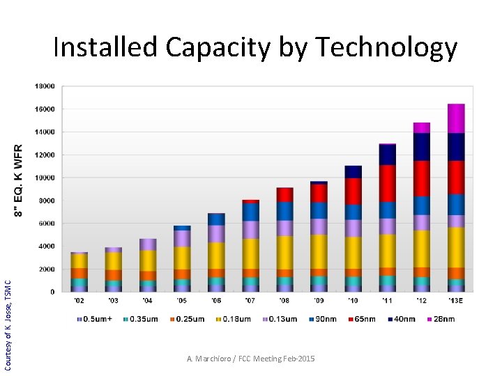
Courtesy of K. Josse, TSMC Installed Capacity by Technology A. Marchioro / FCC Meeting Feb-2015

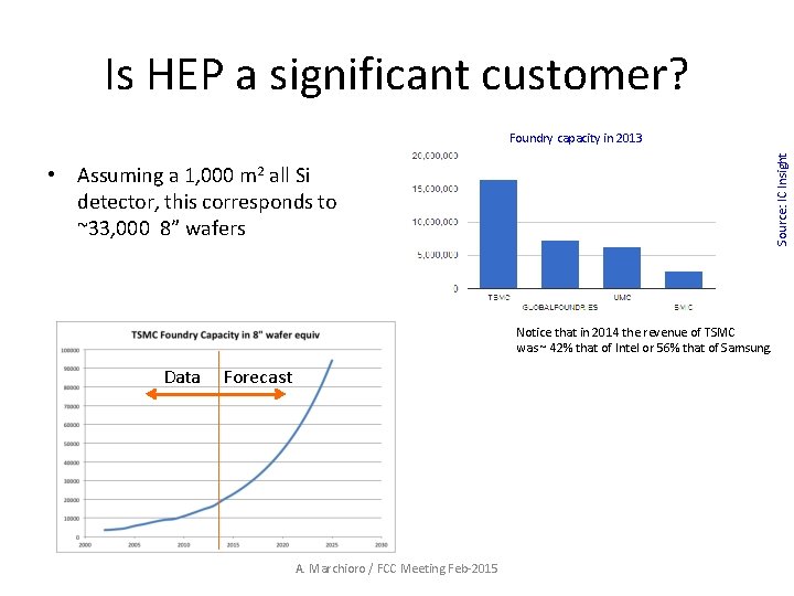
Is HEP a significant customer? Source: IC Insight Foundry capacity in 2013 • Assuming a 1, 000 m 2 all Si detector, this corresponds to ~33, 000 8” wafers Notice that in 2014 the revenue of TSMC was ~ 42% that of Intel or 56% that of Samsung. Data Forecast A. Marchioro / FCC Meeting Feb-2015

INTERCONNECT AND PACKAGING A. Marchioro / FCC Meeting Feb-2015

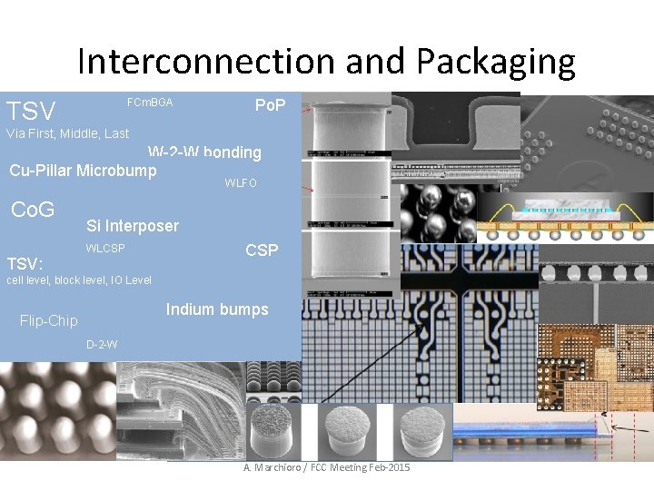
Interconnection and Packaging FCm. BGA TSV Po. P Via First, Middle, Last W-2 -W bonding Cu-Pillar Microbump WLFO Co. G Si Interposer WLCSP TSV: CSP cell level, block level, IO Level Indium bumps Flip-Chip D-2 -W A. Marchioro / FCC Meeting Feb-2015

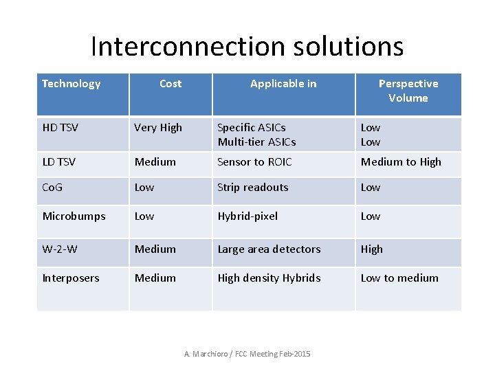
Interconnection solutions Technology Cost Applicable in Perspective Volume HD TSV Very High Specific ASICs Multi-tier ASICs Low LD TSV Medium Sensor to ROIC Medium to High Co. G Low Strip readouts Low Microbumps Low Hybrid-pixel Low W-2 -W Medium Large area detectors High Interposers Medium High density Hybrids Low to medium A. Marchioro / FCC Meeting Feb-2015

With so many solutions, what is the problem? • The variety of packaging solutions offered by industry is staggering and already today widely sufficient for most and perhaps all HEP applications • Except that: – There is a huge fragmentation of suppliers – Entry fees are high – Our volumes are pathetically small A. Marchioro / FCC Meeting Feb-2015

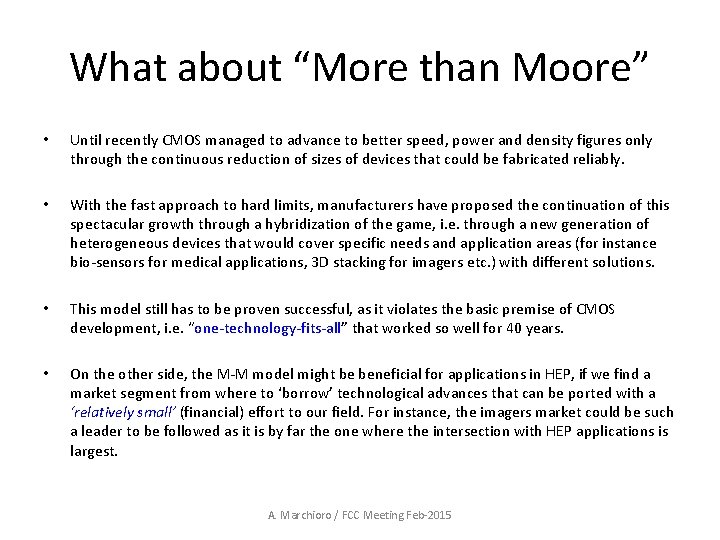
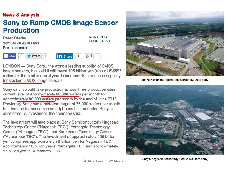
What about “More than Moore” • Until recently CMOS managed to advance to better speed, power and density figures only through the continuous reduction of sizes of devices that could be fabricated reliably. • With the fast approach to hard limits, manufacturers have proposed the continuation of this spectacular growth through a hybridization of the game, i. e. through a new generation of heterogeneous devices that would cover specific needs and application areas (for instance bio-sensors for medical applications, 3 D stacking for imagers etc. ) with different solutions. • This model still has to be proven successful, as it violates the basic premise of CMOS development, i. e. “one-technology-fits-all” that worked so well for 40 years. • On the other side, the M-M model might be beneficial for applications in HEP, if we find a market segment from where to ‘borrow’ technological advances that can be ported with a ‘relatively small’ (financial) effort to our field. For instance, the imagers market could be such a leader to be followed as it is by far the one where the intersection with HEP applications is largest. A. Marchioro / FCC Meeting Feb-2015

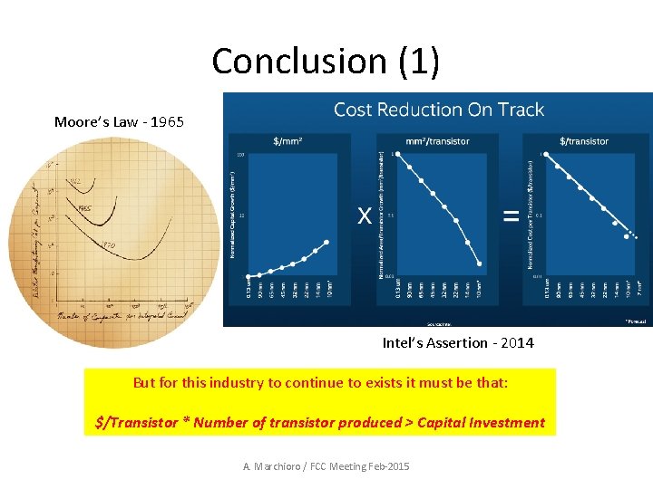
Conclusion (1) Moore’s Law - 1965 Intel’s Assertion - 2014 But for this industry to continue to exists it must be that: $/Transistor * Number of transistor produced > Capital Investment A. Marchioro / FCC Meeting Feb-2015

Conclusion (2) • Pretending to predict what microelectronics will be in > 25 years would simply be ludicrous. – If we look back 25 years (i. e. 1990), none of us could have imagined what technologies we have available today, and not just in semiconductor devices, but mainly in the applications that have created a virtuous cycle of development/investment/new-applications (i. e. Internet, “disposable” computing, telecom, ubiquitous connectivity, cloud) ly certain • Other such technological revolutions are very likely ahead of us and we must be ready to profit from their potential fall-out in our field, i. e. on the new instruments that we could build using such technologies – Beware: Back in 1985 not exactly everybody agreed to start an activity on “microelectronics”, and in fact we had to knock at the door of “visionaries'” to get funded • Real innovation is rarely related to “tech+1”: resources must be allocated to “tech+2”, “tech+3” etc. , with the understanding that some or even most will not be fruitful, but that we can not miss the one that eventually will be successful. A. Marchioro / FCC Meeting Feb-2015

Spare A. Marchioro / FCC Meeting Feb-2015

A. Marchioro / FCC Meeting Feb-2015