Adjustable Linear Range Operational Transconductance Amplifier with Noise
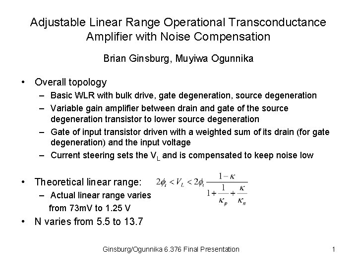
Adjustable Linear Range Operational Transconductance Amplifier with Noise Compensation Brian Ginsburg, Muyiwa Ogunnika • Overall topology – Basic WLR with bulk drive, gate degeneration, source degeneration – Variable gain amplifier between drain and gate of the source degeneration transistor to lower source degeneration – Gate of input transistor driven with a weighted sum of its drain (for gate degeneration) and the input voltage – Current steering sets the VL and is compensated to keep noise low • Theoretical linear range: – Actual linear range varies from 73 m. V to 1. 25 V • N varies from 5. 5 to 13. 7 Ginsburg/Ogunnika 6. 376 Final Presentation 1
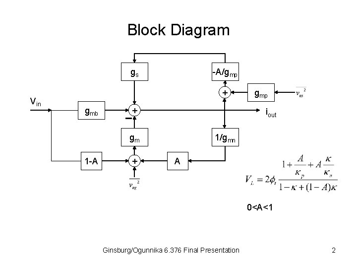
Block Diagram gs Vin -A/gmp + gmb + iout gm 1 -A + gmp 1/gmn A 0<A<1 Ginsburg/Ogunnika 6. 376 Final Presentation 2
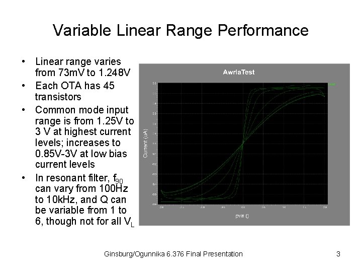
Variable Linear Range Performance • Linear range varies from 73 m. V to 1. 248 V • Each OTA has 45 transistors • Common mode input range is from 1. 25 V to 3 V at highest current levels; increases to 0. 85 V-3 V at low bias current levels • In resonant filter, f 90 can vary from 100 Hz to 10 k. Hz, and Q can be variable from 1 to 6, though not for all VL Ginsburg/Ogunnika 6. 376 Final Presentation 3
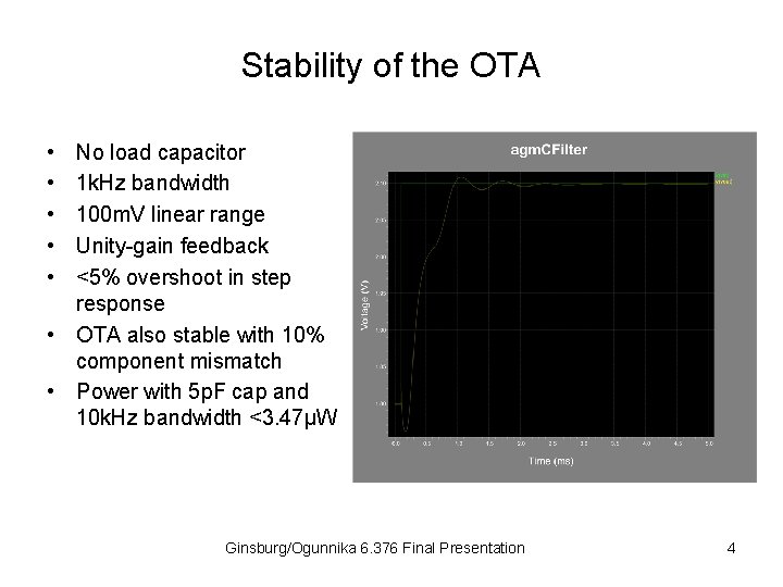
Stability of the OTA • • • No load capacitor 1 k. Hz bandwidth 100 m. V linear range Unity-gain feedback <5% overshoot in step response • OTA also stable with 10% component mismatch • Power with 5 p. F cap and 10 k. Hz bandwidth <3. 47μW Ginsburg/Ogunnika 6. 376 Final Presentation 4
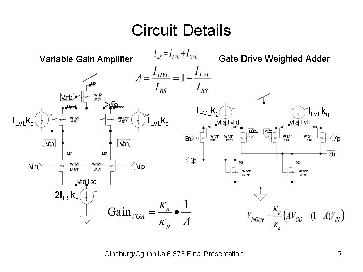
Circuit Details Gate Drive Weighted Adder Variable Gain Amplifier ILVLks IHVLkg ILVLkg 2 IBSks Ginsburg/Ogunnika 6. 376 Final Presentation 5
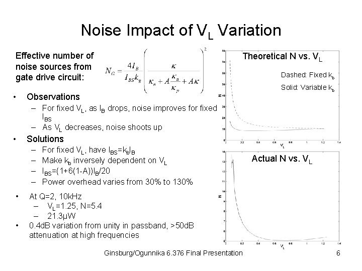
Noise Impact of VL Variation Effective number of noise sources from gate drive circuit: • Theoretical N vs. VL Dashed: Fixed kb Solid: Variable kb Observations – For fixed VL, as IB drops, noise improves for fixed IBS – As VL decreases, noise shoots up • Solutions – – • • For fixed VL, have IBS=kb. IB Make kb inversely dependent on VL IBS=(1+6(1 -A))IB/20 Power overhead varies from 30% to 130% Actual N vs. VL At Q=2, 10 k. Hz – VL=1. 25, N=5. 4 – 21. 3μW 0. 4 d. B variation from unity in passband, >50 d. B attenuation at high frequencies Ginsburg/Ogunnika 6. 376 Final Presentation 6
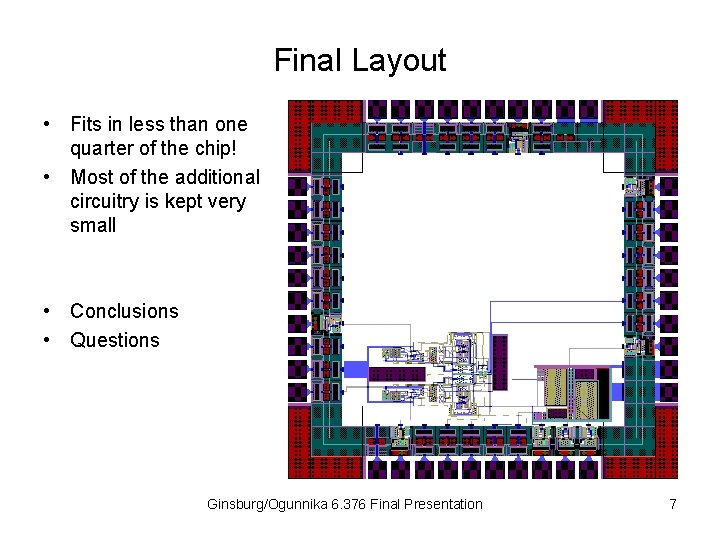
Final Layout • Fits in less than one quarter of the chip! • Most of the additional circuitry is kept very small • Conclusions • Questions Ginsburg/Ogunnika 6. 376 Final Presentation 7
- Slides: 7