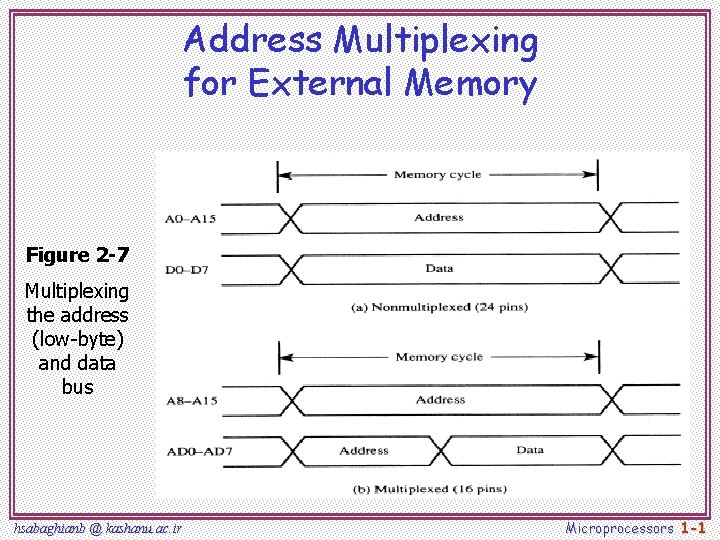
Address Multiplexing for External Memory Figure 2 7
![Register Banks q Active bank selected by PSW [RS 1, RS 0] bit q Register Banks q Active bank selected by PSW [RS 1, RS 0] bit q](https://slidetodoc.com/presentation_image_h/a1842bfd601ae1b359b433c15d9dbc01/image-17.jpg)
- Slides: 18

Address Multiplexing for External Memory Figure 2 -7 Multiplexing the address (low-byte) and data bus hsabaghianb @ kashanu. ac. ir Microprocessors 1 -1

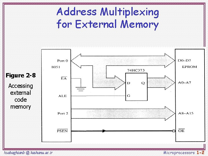
Address Multiplexing for External Memory Figure 2 -8 Accessing external code memory hsabaghianb @ kashanu. ac. ir Microprocessors 1 -2

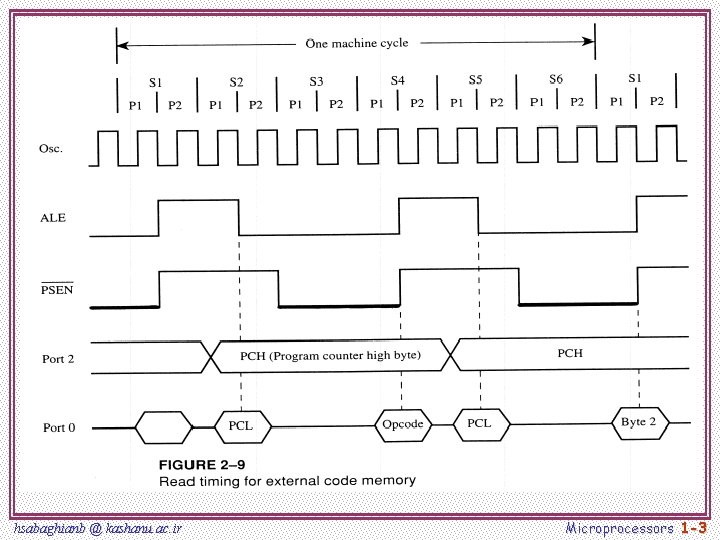
hsabaghianb @ kashanu. ac. ir Microprocessors 1 -3

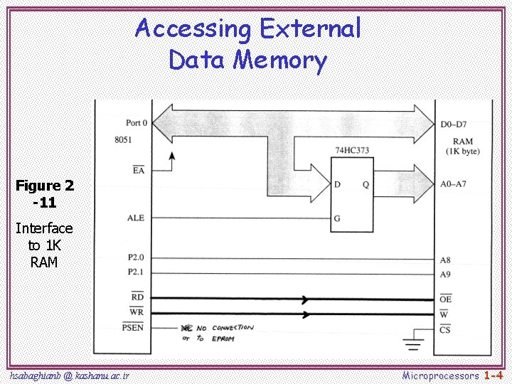
Accessing External Data Memory Figure 2 -11 Interface to 1 K RAM hsabaghianb @ kashanu. ac. ir Microprocessors 1 -4

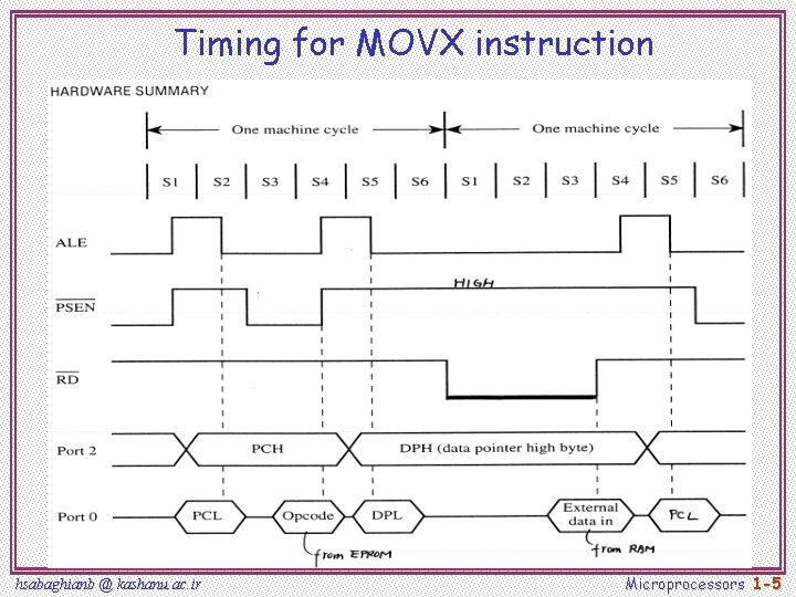
Timing for MOVX instruction hsabaghianb @ kashanu. ac. ir Microprocessors 1 -5

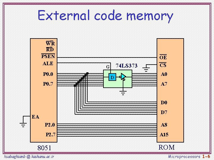
External code memory WR RD PSEN ALE P 0. 0 P 0. 7 74 LS 373 G D OE CS A 0 A 7 D 0 D 7 EA P 2. 0 A 8 P 2. 7 A 15 8051 hsabaghianb @ kashanu. ac. ir ROM Microprocessors 1 -6

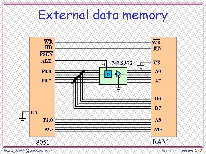
External data memory WR RD PSEN ALE P 0. 0 P 0. 7 WR RD 74 LS 373 G D CS A 0 A 7 D 0 D 7 EA P 2. 0 A 8 P 2. 7 A 15 8051 hsabaghianb @ kashanu. ac. ir RAM Microprocessors 1 -7

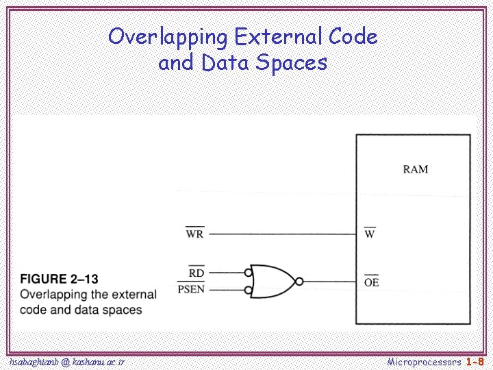
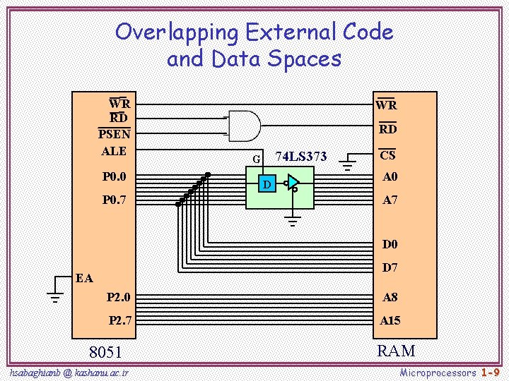
Overlapping External Code and Data Spaces hsabaghianb @ kashanu. ac. ir Microprocessors 1 -8

Overlapping External Code and Data Spaces WR RD PSEN ALE P 0. 0 P 0. 7 WR RD 74 LS 373 G D CS A 0 A 7 D 0 D 7 EA P 2. 0 A 8 P 2. 7 A 15 8051 hsabaghianb @ kashanu. ac. ir RAM Microprocessors 1 -9

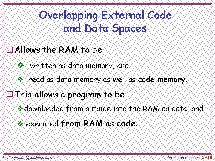
Overlapping External Code and Data Spaces q. Allows the RAM to be v written as data memory, and v read as data memory as well as code memory. q. This allows a program to be vdownloaded from outside into the RAM as data, and v executed from RAM as code. hsabaghianb @ kashanu. ac. ir Microprocessors 1 -10

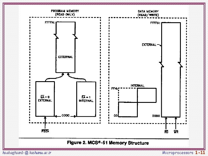
hsabaghianb @ kashanu. ac. ir Microprocessors 1 -11

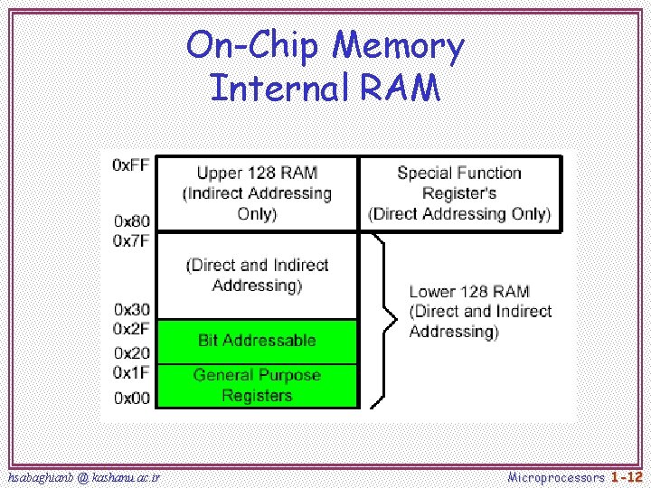
On-Chip Memory Internal RAM hsabaghianb @ kashanu. ac. ir Microprocessors 1 -12

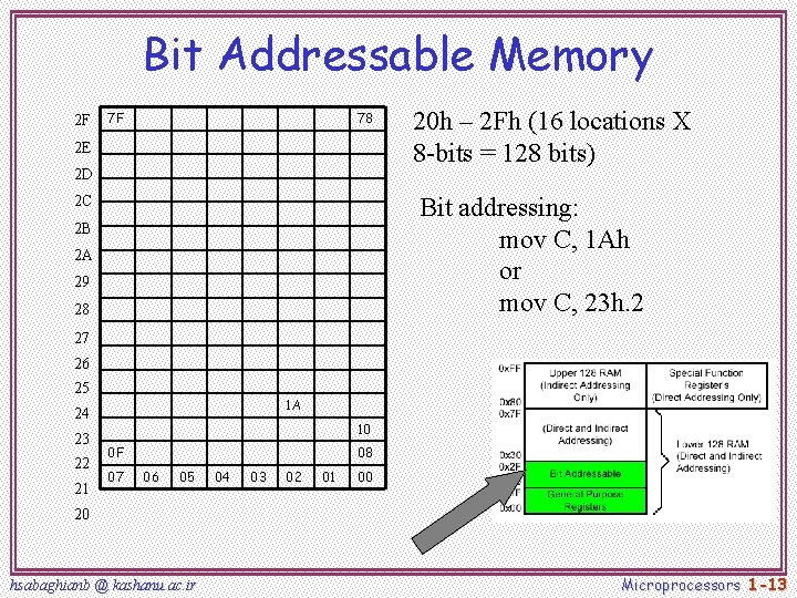
Bit Addressable Memory 2 F 7 F 78 2 E 2 D 20 h – 2 Fh (16 locations X 8 -bits = 128 bits) Bit addressing: mov C, 1 Ah or mov C, 23 h. 2 2 C 2 B 2 A 29 28 27 26 25 1 A 24 23 22 21 10 0 F 07 08 06 05 04 03 02 01 00 20 hsabaghianb @ kashanu. ac. ir Microprocessors 1 -13

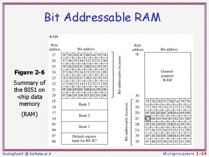
Bit Addressable RAM Figure 2 -6 Summary of the 8051 on -chip data memory (RAM) hsabaghianb @ kashanu. ac. ir Microprocessors 1 -14

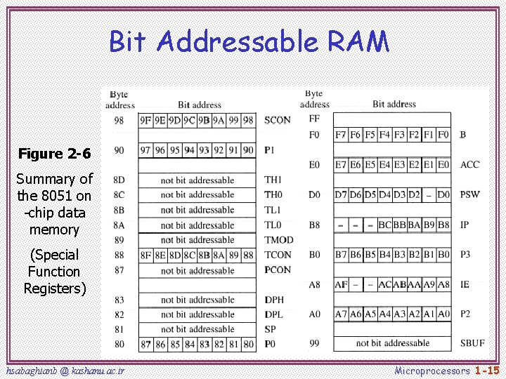
Bit Addressable RAM Figure 2 -6 Summary of the 8051 on -chip data memory (Special Function Registers) hsabaghianb @ kashanu. ac. ir Microprocessors 1 -15

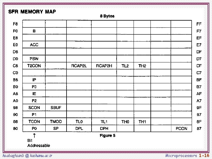
hsabaghianb @ kashanu. ac. ir Microprocessors 1 -16
![Register Banks q Active bank selected by PSW RS 1 RS 0 bit q Register Banks q Active bank selected by PSW [RS 1, RS 0] bit q](https://slidetodoc.com/presentation_image_h/a1842bfd601ae1b359b433c15d9dbc01/image-17.jpg)
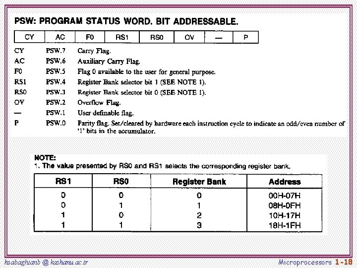
Register Banks q Active bank selected by PSW [RS 1, RS 0] bit q Permits fast “context switching” in interrupt service routines (ISR). hsabaghianb @ kashanu. ac. ir Microprocessors 1 -17

hsabaghianb @ kashanu. ac. ir Microprocessors 1 -18