ADC Board VHDL Firmware development for Mona Lisa

ADC Board VHDL Firmware development for Mona Lisa Roy Wastie

Overview • • Introduction ADC Board Hardware Blocks Basic FPGA Architectures Xilinx ISE 10. 1 Tool Flow USB Algorithm VHDL

Introduction • Applications of FPGAs include digital signal processing, software-defined radio, aerospace and defense systems, ASIC prototyping, medical imaging, computer vision, speech recognition, cryptography, bioinformatics, computer hardware emulation & glue logic for PCBs.

ADC Board

Hardware Blocks External Clock & Trigger 16 channel ADC FIFO FPGA DAQ FPGA Memory controller USB Interface SDRAM Memory

Basic FPGA Architectures

Overview • All Xilinx FPGAs contain the same basic resources – Logic Resources • Slices (grouped into CLBs) – Contain combinatorial logic and register resources • Memory • Multipliers – Interconnect Resources • Programmable interconnect • IOBs – Interface between the FPGA and the outside world – Other resources • Global clock buffers • Boundary scan logic

Basic Building Block Configurable Logic block • Slices contain logic resources and are arranged in two colums • A switch matrix provides access to general routing resources • Local routing provides connection between slices in the same CLB, and it provides routing to neighboring CLBs COUT BUF T COUT Slice S 3 Slice S 2 Switch Matrix SHIFT Slice S 1 Slice S 0 CIN Local Routing CIN Virtex-II CLB contains four slices

Basic Building Blocks Simplified Slice Structure • Each slice has four outputs – Two registered outputs, two non-registered outputs – Two BUFTs associated with each CLB, accessible by all 16 CLB outputs • Carry logic runs vertically, up only – Two independent carry chains per CLB Slice 0 LUT Carry PRE D Q CE CLR LUT Carry D PRE Q CE CLR

The Slice Detailed Structure • The next few slides discuss the slice features – LUTs – MUXF 5, MUXF 6, MUXF 7, MUXF 8 (only the F 5 and F 6 MUX are shown in this diagram) – Carry Logic – MULT_ANDs – Sequential Elements
 • Also called Function")
Combinatorial logic Boolean logic is stored in Look-Up Tables (LUTs) • Also called Function Generators (FGs) • Capacity is limited by the number of inputs, not by the complexity • Delay through the LUT is constant A B C D Z 0 0 0 0 1 1 1 0 0 1 0 1 1 Combinatorial Logic A B C D . Z . . 1 1 0 0 0 1 1 1 0 0 1 1 1

Storage Elements Can be implemented as either flip-flops or latches • Two in each slice; eight in each CLB • Inputs come from LUTs or from an independent CLB input • Separate set and reset controls – Can be synchronous or asynchronous • All controls are shared within a slice – Control signals can be inverted locally within a slice FDRSE_1 D S Q CE R FDCPE D PRE Q CE CLR LDCPE D PRE Q CE G CLR

Dedicated Logic FPGAs contain built-in logic for speeding up logic operations and saving • Multiplexer Logic – Connect Slices and LUTs • Carry Chains – Speed up arithmetic operations • Multiplier AND gate – Speed up LUT-based multiplication • Shift Register LUT – LUT-based shift register • Embedded Multiplier – 18 x 18 Multiplier

Multiplexer Logic Dedicated MUXes provided to connect slices and LUTs F 6 Slice S 0 F 5 Slice S 1 F 5 F 7 Slice S 2 F 5 F 6 Slice S 3 F 5 F 8 CLB MUXF 8 combines the two MUXF 7 outputs (from the CLB above or below) MUXF 6 combines slices S 2 and S 3 MUXF 7 combines the two MUXF 6 outputs MUXF 6 combines slices S 0 and S 1 MUXF 5 combines LUTs in each slice

Carry Chains Dedicated carry chains speeds up arithmetic operations • Simple, fast, and complete arithmetic Logic – Dedicated XOR gate for single-level sum completion – Uses dedicated routing resources – All synthesis tools can infer carry logic COUT To S 0 of the next CLB To CIN of S 2 of the next CLB First Carry Chain SLICE S 3 CIN COUT SLICE S 2 SLICE S 1 CIN Second Carry Chain COUT SLICE S 0 CIN CLB

Multiplier AND Gate Speed up LUT-based multiplication • Highly efficient multiply and add implementation – Earlier FPGA architectures require two LUTs per bit to perform the multiplication and addition – The MULT_AND gate enables an area reduction by performing the multiply and the add in one LUT per bit LUT A CY_MUX S CO DI CI CY_XOR MULT_AND A x B LUT
 The shift register LUT saves from having to")
Shift Register LUT (SRL 16 CE) The shift register LUT saves from having to use dedicated registers • Dynamically addressable serial shift registers – Maximum delay of 16 clock cycles per LUT (128 per CLB) – Cascadable to other LUTs or CLBs for longer shift registers LUT D CE CLK D Q CE • Dedicated connection from Q 15 to D input of the next LUT SRL 16 CE – Shift register length can be changed asynchronously by toggling address A D Q CE Q D Q CE A[3: 0] Q 15 (cascade out)

Embedded Multiplier Blocks Saves from having to use LUTs to implement multiplications and increases p • 18 -bit twos complement signed operation • Optimized to implement Multiply and Accumulate functions • Multipliers are physically located next to block Select. RAM™ memory Data_A (18 bits) 4 x 4 signed 18 x 18 Multiplier Data_B (18 bits) Output (36 bits) 8 x 8 signed 12 x 12 signed 18 x 18 signed

IOB Element Connects the FPGA design to external components • Input path IOB – Two DDR registers • Output path – Two DDR registers – Two 3 -state enable DDR registers • Separate clocks and clock enables for I and O • Set and reset signals are shared Reg DDR MUX OCK 1 Input Reg ICK 1 Reg OCK 2 3 -state Reg ICK 2 Reg DDR MUX OCK 1 Reg OCK 2 PAD Output

Distributed RAM Uses a LUT in a slice as memory • Synchronous write • Asynchronous read – Accompanying flip-flops can be used to create synchronous read • RAM and ROM are initialized during configuration – Data can be written to RAM after configuration • Emulated dual-port RAM – One read/write port – One read-only port • 1 LUT = 16 RAM bits LUT Slice LUT RAM 16 X 1 S D WE WCLK A 0 O A 1 A 2 A 3 RAM 32 X 1 S D WE WCLK A 0 O A 1 A 2 A 3 A 4 RAM 16 X 1 D D WE WCLK A 0 SPO A 1 A 2 A 3 DPRA 0 DPO DPRA 1 DPRA 2 DPRA 3

Block RAM Embedded blocks of RAM arranged in columns • Up to 3. 5 Mb of RAM in 18 -kb blocks – Synchronous read and write • True dual-port memory – Each port has synchronous read and write capability – Different clocks for each port • Supports initial values • Synchronous reset on output latches • Supports parity bits – One parity bit per eight data bits • Situated next to embedded multiplier 18 -kb block Select. RAM memory DIA DIPA ADDRA WEA ENA SSRA CLKA DOPA DIB DIPB ADDRB WEB ENB SSRB CLKB DOPB

Global Routing • Sixteen dedicated global clock multiplexers – Eight on the top-center of the die, eight on the bottom-center – Driven by a clock input pad, a DCM, or local routing • Global clock multiplexers provide the following: – Traditional clock buffer (BUFG) function – Global clock enable capability (BUFGCE) – Glitch-free switching between clock signals (BUFGMUX) • Up to eight clock nets can be used in each clock region of the device – Each device contains four or more clock regions
 • Up to twelve DCMs per device – Located on")
Digital Clock Manager (DCM) • Up to twelve DCMs per device – Located on the top and bottom edges of the die – Driven by clock input pads • DCMs provide the following: – Delay-Locked Loop (DLL) – Digital Frequency Synthesizer (DFS) – Digital Phase Shifter (DPS) • Up to four outputs of each DCM can drive onto global clock buffers – All DCM outputs can drive general routing

The. Built Spartan-3 Family for high volume, low-cost applications 18 x 18 bit Embedded Pipelined Multipliers for efficient DSP Configurable 18 K Block RAMs + Distributed RAM Bank 0 Bank 2 Bank 1 Up to eight on-chip Digital Clock Managers to support multiple system clocks Bank 3 Spartan-3 4 I/O Banks, Support for all I/O Standards including PCI, DDR 333, RSDS, mini-LVDS

Spartan-3 Family Based upon Virtex-II Architecture – Optimized for Lower Cost • Smaller process = lower core voltage –. 09 micron versus. 15 micron – Vccint = 1. 2 V versus 1. 5 V • Logic resources – Only one-half of the slices support RAM or SRL 16 s (SLICEM) – Fewer block RAMs and multiplier blocks • Clock Resources – Fewer global clock multiplexers and DCM blocks • I/O Resources – Fewer pins per package – No internal 3 -state buffers – Support for different standards • New standards: 1. 2 V LVCMOS, 1. 8 V HSTL, and SSTL • Default is LVCMOS, versus LVTTL

SLICEM and SLICEL • Each Spartan™-3 CLB contains four slices Right-Hand SLICEL Left-Hand SLICEM COUT – Similar to the Virtex™-II Slice X 1 Y 1 • Slices are grouped in pairs – Left-hand SLICEM (Memory) • LUTs can be configured as memory or SRL 16 – Right-hand SLICEL (Logic) • LUT can be used as logic only Slice X 1 Y 0 Switch Matrix SHIFTIN Slice X 0 Y 1 Fast Connect Slice X 0 Y 0 SHIFTOUT CIN

Xilinx Tool Flow

Xilinx Design Flow Plan & Budget Create Code/ Schematic HDL RTL Simulation Implement Translate Functional Simulation Synthesize to create netlist Map Place & Route Attain Timing Closure Timing Simulation Generate BIT File Configure FPGA

Synthesis Generate a netlist file • After coding up your HDL code, you will need a tool to generate a netlist (NGC or EDIF) – Xilinx Synthesis Tool (XST) included – Support for Popular Third Party Synthesis tools: Synplify, Leonardo Spectrum

Implementation Process a netlist file • Consists of three phases – Translate: Merge multiple design files into a single netlist – Map: Group logical symbols from the netlist (gates) into physical components (slices and IOBs) – Place & Route: Place components onto the chip, connect the components, and extract timing data into reports • Access Xilinx reports and tools at each phase – Timing Analyzer, Floorplanner, FPGA Editor, XPower Netlist Generated From Synthesis. . . Implement Translate Map Place & Route. . .

Configuration • Once a design is implemented, you must create a file that the FPGA can understand – This file is called a bitstream: a BIT file (. bit extension) • The BIT file can be downloaded – Directly into the FPGA • Use a download cable such as Platform USB – To external memory device such as a Xilinx Platform Flash PROM • Must first be converted into a PROM file

ISE Project Navigator Xilinx ISE Foundation is built around the Xilinx Design Flow • Enter Designs • Access to synthesis tools – Including third-party synthesis tools • Implement your design with a simple double-click – Fine-tune with easy-to-access software options • Download – Generate a bitstream – Configure FPGA using
 Synthesis Processes and")
Synthesizing Designs Generate a netlist file using XST (Xilinx Synthesis Technology) Synthesis Processes and Analysis • Access report • View Schematics (RTL or Technology) • Check syntax • Generate Post-Synthesis Simulation Model 1 Highlight HDL Sources 2 Double-click to Synthesize

The Design Summary Displays Design Data • Quick View of Reports, Constraints • Project Status • Device Utilization • Design Summary Options • Performance and Constraints • Reports

Outline • • Overview ISE Summary Lab 1: Xilinx Tool Flow

USB

USB 2 • • Peer to Peer. Host computer is master. 480 Mbits/s 53. 24 Mb/s theoretical 30 MB/s readily achievable in Bulk transfer mode. The speeds USB 1. 0 Low & Full , USB 2 High Hot Plug. Peripherals electronics can be relatively simple and inexpensive. • Power 500 m. A from the bus.
 • Token packet")
USB Data Travels in Packets • Identified by “Packet ID” (PID) • Token packet tells what’s coming • Data packets deliver bytes • Handshake packets report success or otherwise

USB Packets S S E Y T N U C P A D D R E N D P D S A Y T N A C 0 C R C 5 Token Packet C R C 1 6 Data Packet S A Y C N K C S O Y U N T C H/S Pkt Data Packet C R C 1 6 S A Y C N K C C R C 5 Data Stage S O Y U N T C H/S Pkt E N D P Token Packet Setup Stage D S A Y T N A C 1 A D D R E N D P D S A Y T N A C 0 C R C 5 Token Packet C R C 1 6 Data Packet S A Y C N K C H/S Pkt Data Stage (cont'd) S O Y U N T C A E C D N R D D C R P 5 Token Packet D C S D A R Y a T C N t A 1 C a 1 6 S A Y C N K C Data Packet H/S Pkt Data Stage (cont'd) S Y I N N C A D D R E N D P C R C 5 Token Packet D C S A R Y T C N A 1 C 1 6 Data Packet H/S Pkt Status Stage A Control Write Transfer S A Y C N K C
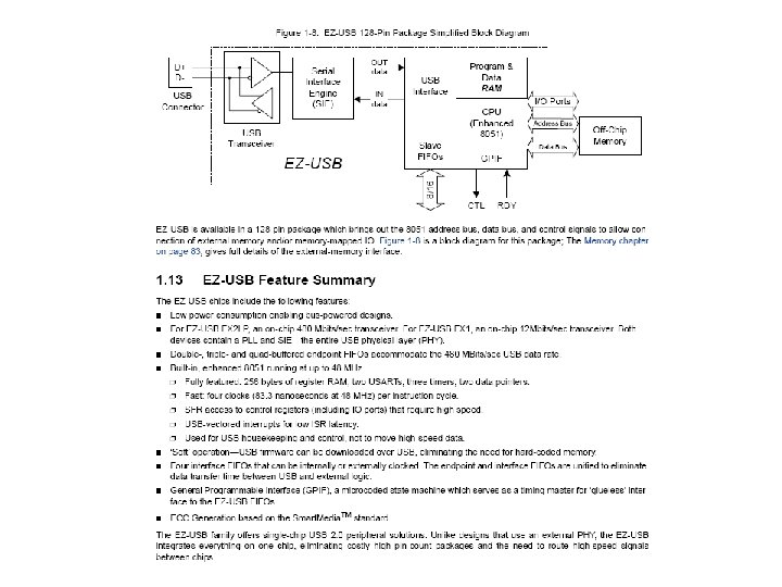
 USB Microcontroller High-Speed USB Peripheral Controller")
USB 2 Controller • EZ-USB FX 2 LP(TM) USB Microcontroller High-Speed USB Peripheral Controller • Integrated 8051 Microprocessor. • Code/Data Downloaded via USB, or EEPROM. • Many Integrated Peripherals.
 •")
Simple Algorithm • Sample Data at full rate 2. 77 Ms/s (16 channels) • Down Convert Data to by 4 • Write data to USB interface 21. 19 MB/s

VHDL

VHDL Example An example of a two-input XNOR gate is shown below. entity XNOR 2 is port (A, B: in std_logic; Z: out std_logic); end XNOR 2; architecture behavioral_xnor of XNOR 2 is -- signal declaration (of internal signals X, Y) signal X, Y: std_logic; begin X <= A and B; Y <= (not A) and (not B); Z <= X or Y; End behavioral_xnor;

- Slides: 45