ADC 32 RF 45 with KCU 105 Internal
- Slides: 12

ADC 32 RF 45 with KCU 105 Internal Clock Fs @ 1. 536 GHz

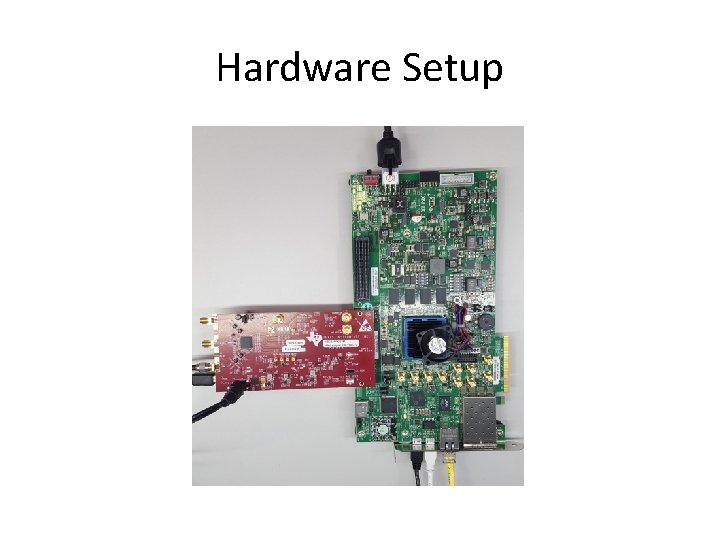
Hardware Setup

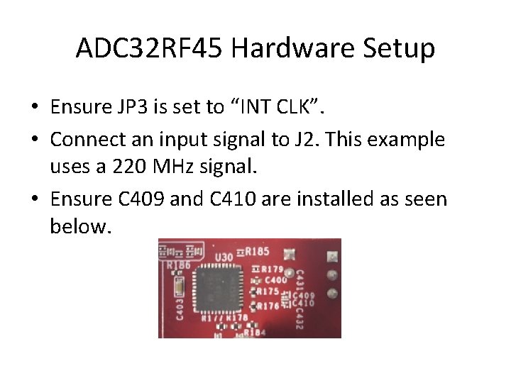
ADC 32 RF 45 Hardware Setup • Ensure JP 3 is set to “INT CLK”. • Connect an input signal to J 2. This example uses a 220 MHz signal. • Ensure C 409 and C 410 are installed as seen below.

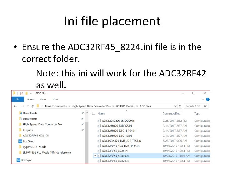
Ini file placement • Ensure the ADC 32 RF 45_8224. ini file is in the correct folder. Note: this ini will work for the ADC 32 RF 42 as well.

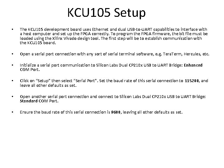
KCU 105 Setup • • The KCU 105 development board uses Ethernet and dual USB-to-UART capabilities to interface with a host computer and set up the FPGA correctly. To program the FPGA firmware, the bit file must be loaded using the Xilinx Vivado design tool. The first step will be to establish communication with the KCU 105 board. Open a serial port connection with any sort of serial terminal software, e. g. Tera. Term, Hercules, etc. • Initialize a serial port communication to Silicon Labs Dual CP 210 x USB to UART Bridge: Enhanced COM Port. • Click on “Setup” then select “Serial Port”. Set the baud rate of this serial connection to 115200, and leave all other defaults as set. • Open another serial port connection and connect to Silicon Labs Dual CP 210 x USB to UART Bridge: Standard COM Port. • Ensure the baud rate of this serial connection is 9600, leaving all other defaults as set.

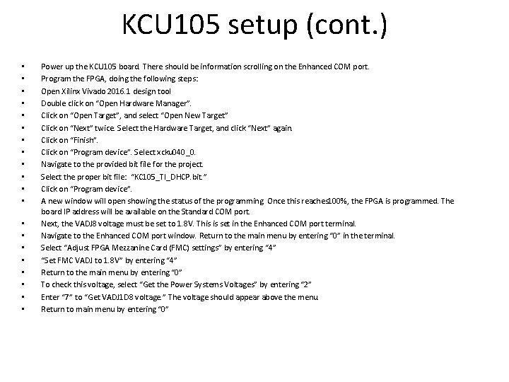
KCU 105 setup (cont. ) • • • • • Power up the KCU 105 board. There should be information scrolling on the Enhanced COM port. Program the FPGA, doing the following steps: Open Xilinx Vivado 2016. 1 design tool Double click on “Open Hardware Manager”. Click on “Open Target”, and select “Open New Target” Click on “Next” twice. Select the Hardware Target, and click “Next” again. Click on “Finish”. Click on “Program device”. Select xcku 040_0. Navigate to the provided bit file for the project. Select the proper bit file: “KC 105_TI_DHCP. bit. ” Click on “Program device”. A new window will open showing the status of the programming. Once this reaches 100%, the FPGA is programmed. The board IP address will be available on the Standard COM port. Next, the VADJ 8 voltage must be set to 1. 8 V. This is set in the Enhanced COM port terminal. Navigate to the Enhanced COM port window. Return to the main menu by entering “ 0” in the terminal. Select “Adjust FPGA Mezzanine Card (FMC) settings” by entering “ 4” “Set FMC VADJ to 1. 8 V” by entering “ 4” Return to the main menu by entering “ 0” To check this voltage, select “Get the Power Systems Voltages” by entering “ 2” Enter “ 7” to “Get VADJ 1 D 8 voltage. ” The voltage should appear above the menu. Return to main menu by entering “ 0”

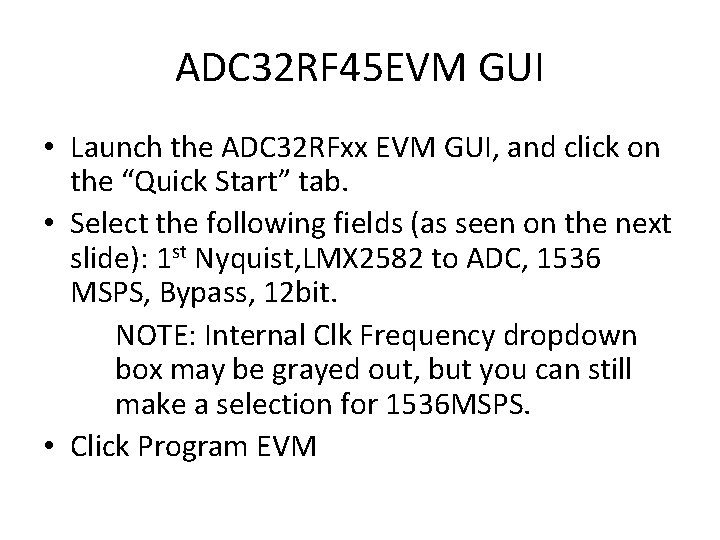
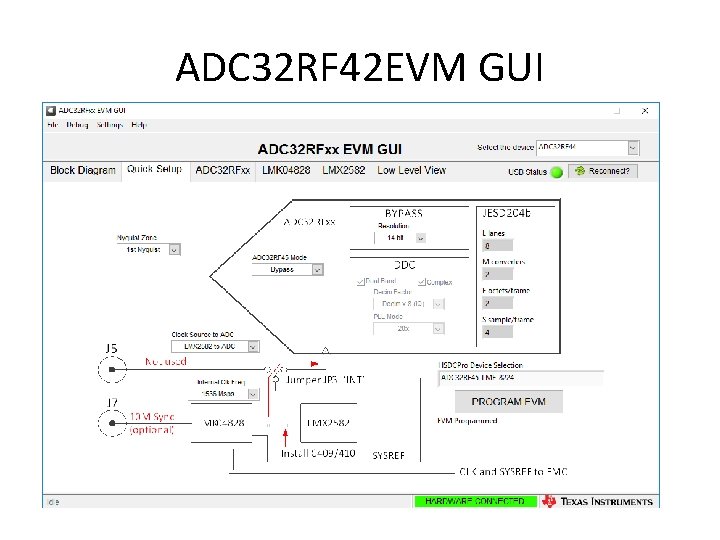
ADC 32 RF 45 EVM GUI • Launch the ADC 32 RFxx EVM GUI, and click on the “Quick Start” tab. • Select the following fields (as seen on the next slide): 1 st Nyquist, LMX 2582 to ADC, 1536 MSPS, Bypass, 12 bit. NOTE: Internal Clk Frequency dropdown box may be grayed out, but you can still make a selection for 1536 MSPS. • Click Program EVM

ADC 32 RF 42 EVM GUI

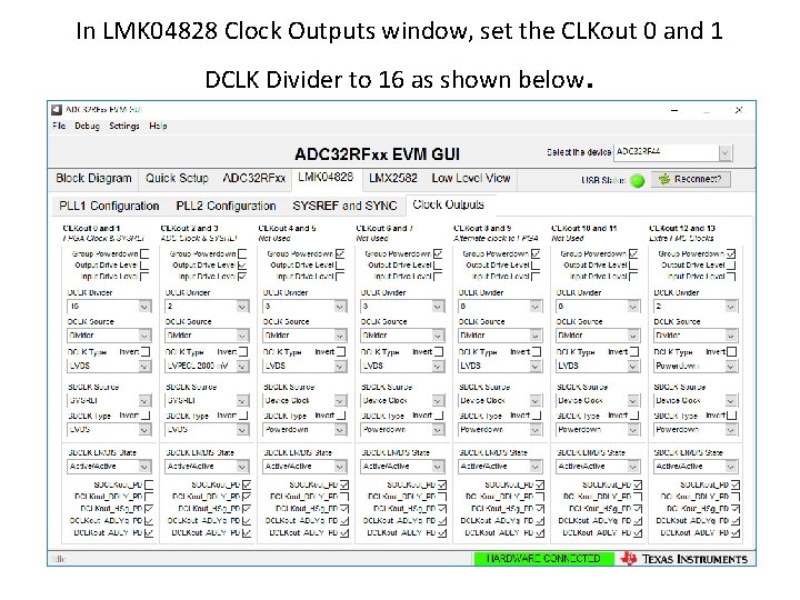
In LMK 04828 Clock Outputs window, set the CLKout 0 and 1 DCLK Divider to 16 as shown below .

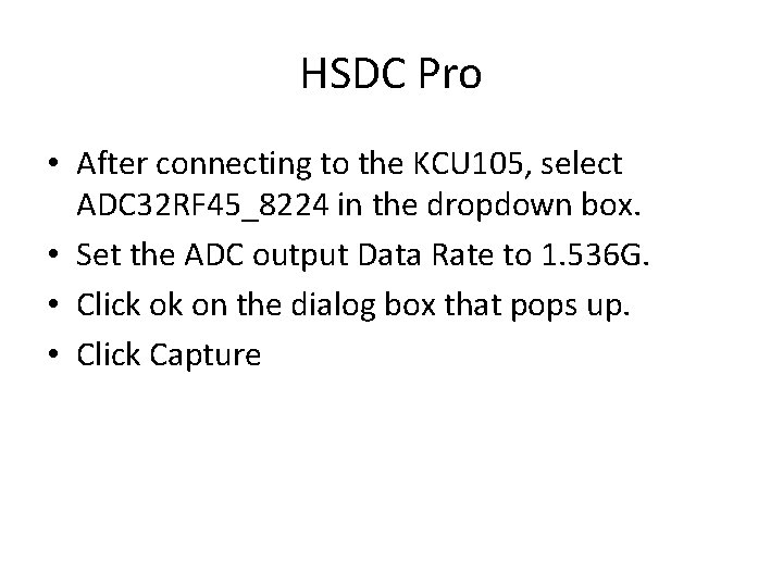
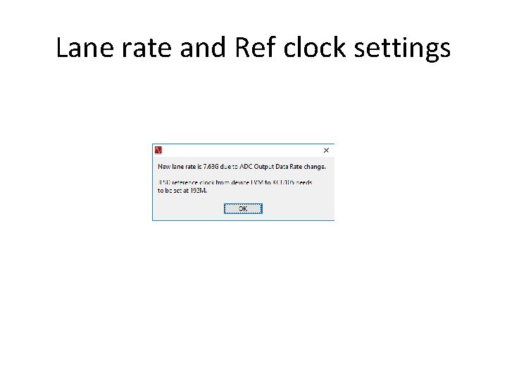
HSDC Pro • After connecting to the KCU 105, select ADC 32 RF 45_8224 in the dropdown box. • Set the ADC output Data Rate to 1. 536 G. • Click ok on the dialog box that pops up. • Click Capture

Lane rate and Ref clock settings

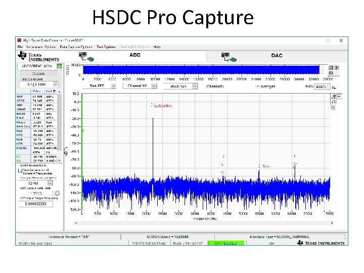
HSDC Pro Capture