Adaptive Differential Pulse Code Modulation DecoderEncoder Hardware Implementation
- Slides: 14

Adaptive Differential Pulse Code Modulation Decoder/Encoder Hardware Implementation Adam Kaplan Serge Baltayan CS 151 C Final Presentation March 23 rd, 2004 3/23/2004 CS 151 C Final Project 1/14

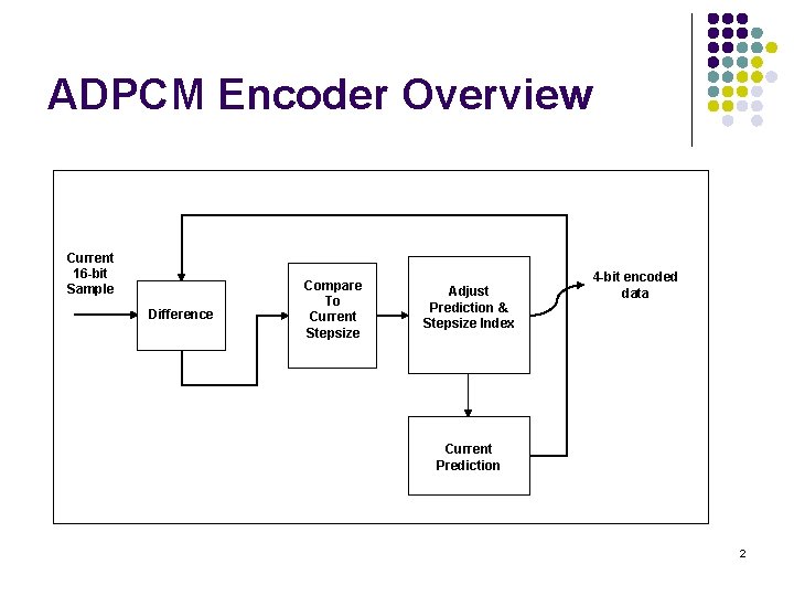
ADPCM Encoder Overview Current 16 -bit Sample Difference Compare To Current Stepsize Adjust Prediction & Stepsize Index 4 -bit encoded data Current Prediction 2

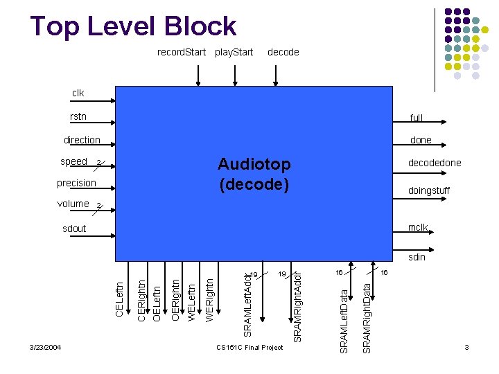
Top Level Block record. Start play. Start decode clk rstn full direction speed done Audiotop (decode) 2 precision volume decodedone doingstuff 2 mclk sdout CS 151 C Final Project 16 16 SRAMRight. Data SRAMLeft. Addr WERightn WELeftn OERightn OELeftn 19 SRAMLeft. Data 3/23/2004 CERightn CELeftn 19 SRAMRight. Addr sdin 3

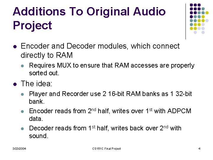
Additions To Original Audio Project l Encoder and Decoder modules, which connect directly to RAM l l Requires MUX to ensure that RAM accesses are properly sorted out. The idea: l l l 3/23/2004 Player and Recorder use 2 16 -bit RAM banks as 1 32 -bit bank. Encoder reads from 2 nd half, writes over 1 st with ADPCM data. Decoder reads from 1 st half, writes back over 2 nd with sound. CS 151 C Final Project 4

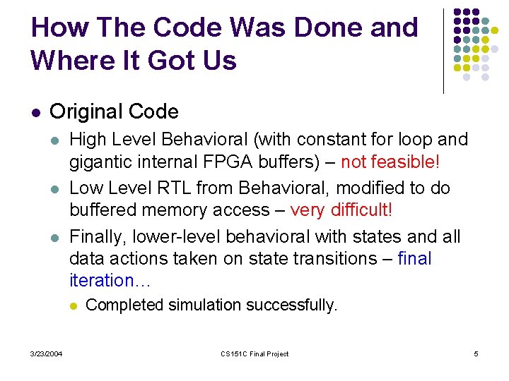
How The Code Was Done and Where It Got Us l Original Code l l l High Level Behavioral (with constant for loop and gigantic internal FPGA buffers) – not feasible! Low Level RTL from Behavioral, modified to do buffered memory access – very difficult! Finally, lower-level behavioral with states and all data actions taken on state transitions – final iteration… l 3/23/2004 Completed simulation successfully. CS 151 C Final Project 5

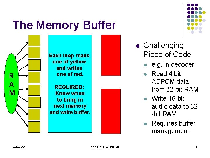
The Memory Buffer l R A M Each loop reads one of yellow and writes one of red. Challenging Piece of Code l l REQUIRED: Know when to bring in next memory and write buffer. l l 3/23/2004 CS 151 C Final Project e. g. in decoder Read 4 bit ADPCM data from 32 -bit RAM Write 16 -bit audio data to 32 -bit RAM Requires buffer management! 6

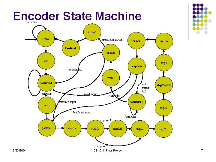
Encoder State Machine ‘encode fixbuf swait finished w/RAM step 5 b step 5 a flushbuf upaddr init step 4 step 5 c/6 need input write waitread canread need input out buffer full step 2 with 3 canwrite buffered input waitwrite read step 2 c buffered input ‘canwrite sign = ‘ 1’ postram 3/23/2004 step 1 a step 1 b negdiff sign = ‘ 0’ CS 151 C Final Project step 2 a step 2 b 7

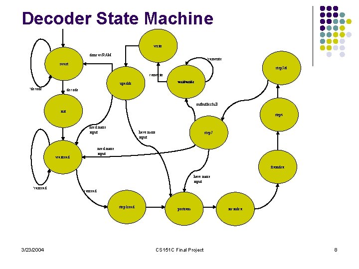
Decoder State Machine write done w/RAM ‘canwrite swait step 5/6 canwrite waitwrite upaddr ‘decode outbuffer full init step 4 need more input have more input step 7 need more input waitread fixindex have more input ‘canread step 1 read 3/23/2004 postram CS 151 C Final Project incindex 8

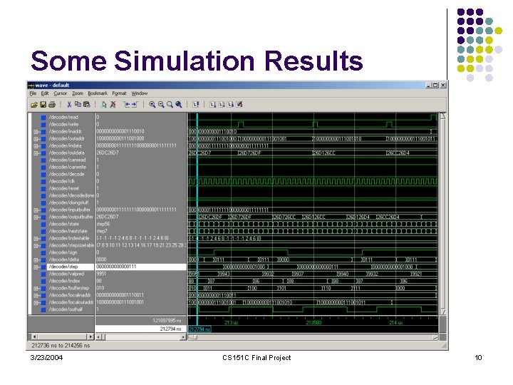
Verifying Functionality l Required: l l Must know that control path is working Must know that buffer is working Must know that output is correctly generated Simulation Results Verify All of Above 3/23/2004 CS 151 C Final Project 9

Some Simulation Results 3/23/2004 CS 151 C Final Project 10

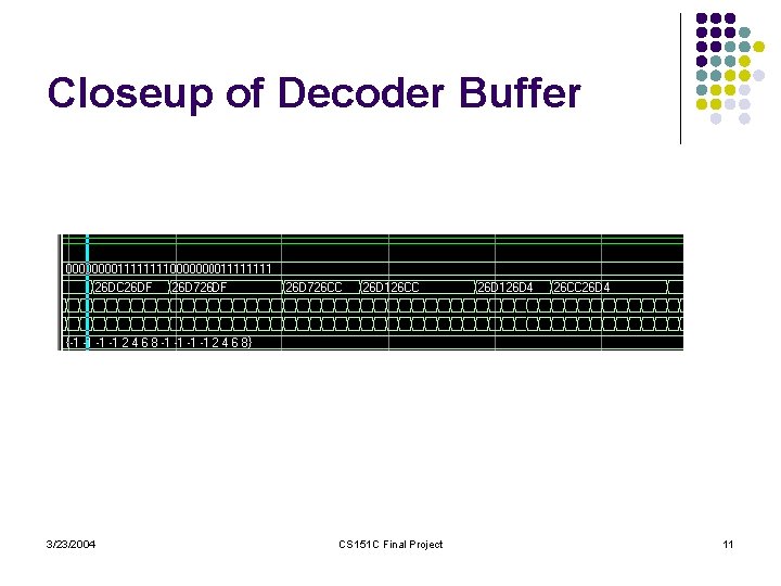
Closeup of Decoder Buffer 3/23/2004 CS 151 C Final Project 11

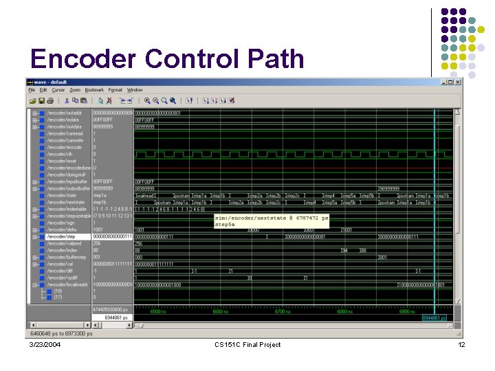
Encoder Control Path 3/23/2004 CS 151 C Final Project 12

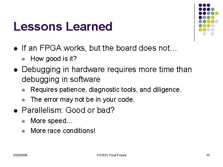
Lessons Learned l If an FPGA works, but the board does not… l l Debugging in hardware requires more time than debugging in software l l l How good is it? Requires patience, diagnostic tools, and diligence. The error may not be in your code. Parallelism: Good or bad? l l 3/23/2004 More speed… More race conditions! CS 151 C Final Project 13

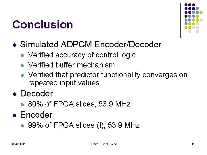
Conclusion l Simulated ADPCM Encoder/Decoder l l Verified accuracy of control logic Verified buffer mechanism Verified that predictor functionality converges on repeated input values. 80% of FPGA slices, 53. 9 MHz Encoder l 3/23/2004 99% of FPGA slices (!), 53. 9 MHz CS 151 C Final Project 14