Activitats en Nanotecnologies Grup de Dispositius Sensors i
- Slides: 11

Activitats en Nanotecnologies Grup de Dispositius, Sensors i Disseny VLSI Eduard Llobet Lluís F. Marsal 1/11

Sub-línies • MINOS: Microsystems and Nanotechnologies for Chemical Analysis (4 permanent, 2 RC, 1 JC, 9 Ph. D students) – Nanosized metal oxide films for gas sensors – CNT based gas sensors – Porous alumina as template material • NEPHOS: Nano Electronic and Photonic Systems ( 4 permanent, 1 RC, 1 JC, 8 Ph. D students) – Modeling of nanoscale MOSFETs – Porous and macroporous silicon – Photonic crystals 2/11

Projectes • Desarrollo de tecnología para células solares fotovoltaicas TIC 2002 -4184 -C 02 -02, 2003 -2005 • SINANO E 04003 S • EUROSOI E 04002 S • Food Quality and Safety with Microsystems, Good. Food FP 6 -IST -1 -508774 -IP, 2003 -2006 • Técnicas y tecnologías para el desarrollo de microsistemas analizadores de gases basados en agrupaciones integradas de sensores catalíticos TIC 2003 -06301, 2004 -2006 3/11

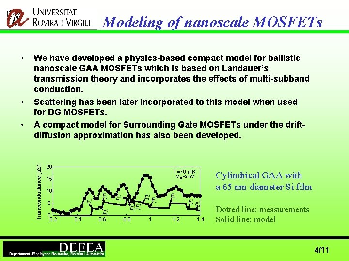
Modeling of nanoscale MOSFETs • • We have developed a physics-based compact model for ballistic nanoscale GAA MOSFETs which is based on Landauer’s transmission theory and incorporates the effects of multi-subband conduction. Scattering has been later incorporated to this model when used for DG MOSFETs. A compact model for Surrounding Gate MOSFETs under the driftdiffusion approximation has also been developed. Transconductance ( S) • 20 T=70 m. K Cylindrical GAA with a 65 nm diameter Si film VDS=2 m. V 15 10 5 0 0. 2 0. 4 0. 6 0. 8 1 1. 2 1. 4 Dotted line: measurements Solid line: model 4/11

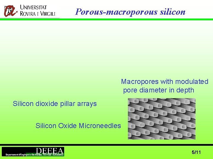
Porous-macroporous silicon Macropores with modulated pore diameter in depth Silicon dioxide pillar arrays Silicon Oxide Microneedles 5/11

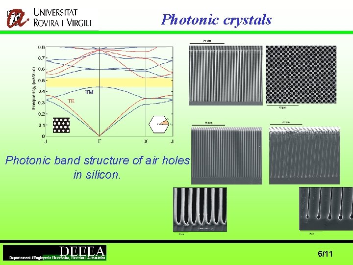
Photonic crystals Photonic band structure of air holes in silicon. 6/11

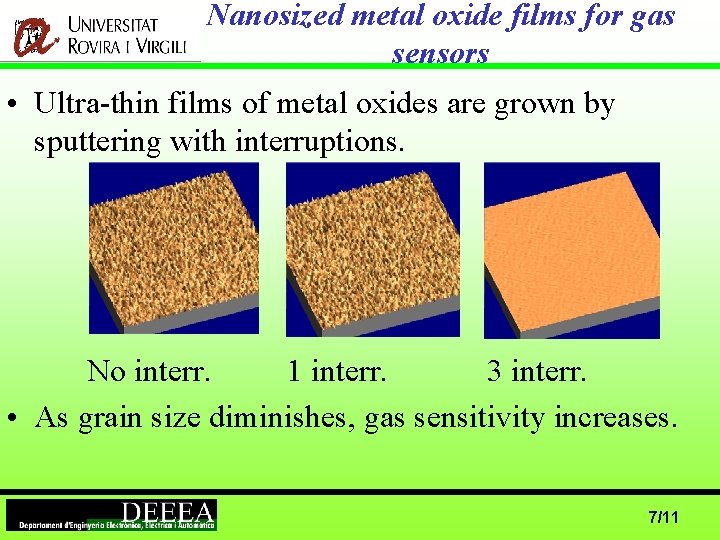
Nanosized metal oxide films for gas sensors • Ultra-thin films of metal oxides are grown by sputtering with interruptions. No interr. 1 interr. 3 interr. • As grain size diminishes, gas sensitivity increases. 7/11

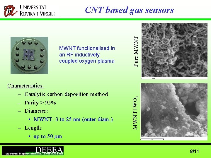
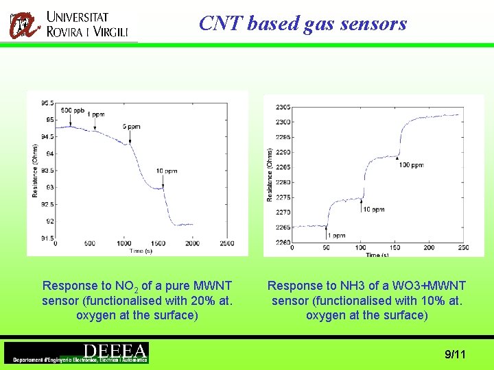
Characteristics: – Catalytic carbon deposition method – Purity > 95% – Diameter: • MWNT: 3 to 25 nm (outer diam. ) – Length: • up to 50 m MWNT+WO 3 MWNT functionalised in an RF inductively coupled oxygen plasma Pure MWNT CNT based gas sensors 8/11

CNT based gas sensors Response to NO 2 of a pure MWNT sensor (functionalised with 20% at. oxygen at the surface) Response to NH 3 of a WO 3+MWNT sensor (functionalised with 10% at. oxygen at the surface) 9/11

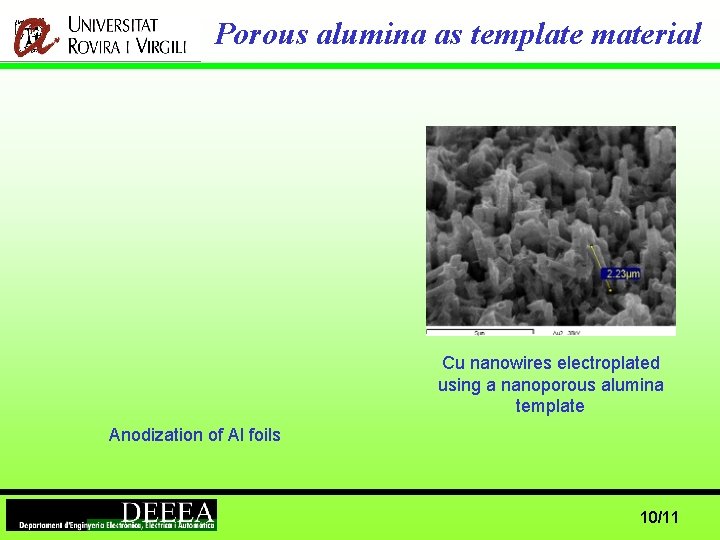
Porous alumina as template material Cu nanowires electroplated using a nanoporous alumina template Anodization of Al foils 10/11

Publicacions rellevants • • • Modeling of Nanoscale Gate-All-Around MOSFETs, IEEE Electron Device Letters, 2004 Analysis of photonic band gaps in two-dimensional photonic crystals with rods covered by a thin interfacial layer, Phys. Rev. B, 2004 Continuous analytic current-voltage model for surrounding gate MOSFETs, IEEE Electron Device Letters, 2004 Effects of symmetry reduction in two-dimensional square and triangular lattices, Phys. Rev. B, 2004 Detection of NO 2 and NH 3 with Oxygen Functionalised MWNT-based hotplate gas sensors, Eurosensors XVIII, 2004 and submitted to Sensors Actuators B. New Technology of Metal Oxide Thin Film Preparation for Chemical Sensor Application, presented at E-MRS 2004 and submitted to Sensors Actuators B. 11/11