Active doping profile using Transmission Line Matrix method


- Slides: 36

Active doping profile using Transmission Line Matrix method A. Lounis*, E. Gkougkoussis 1, T. Rashid**, S. Zacharias*** Jean Luc Perrossier 2, J. R coudeyville 2, C. Villebasse 2, Basics of TLM The methodology Results of doping profile Conclusions * Université de Paris-Sud XI, Laboratoire de l’Accélérateur Linéaire ** Phd student Université de Paris-sud XI, Orsay *** Master 1 Student, Université de Paris Sud XI-Orsay 1 CNM Barcelona 2 Institut Electronique Fondamentale, Orsay ABDENOUR LOUNIS, RD 50 CERN, 20 NOVEMBER 2017 1

5 What is the TLM method? TLM method ( Transmission Line Matrix method) based on measuring the resistance of doped silicon layers at depths increasing incrementally in the implanted area. ND

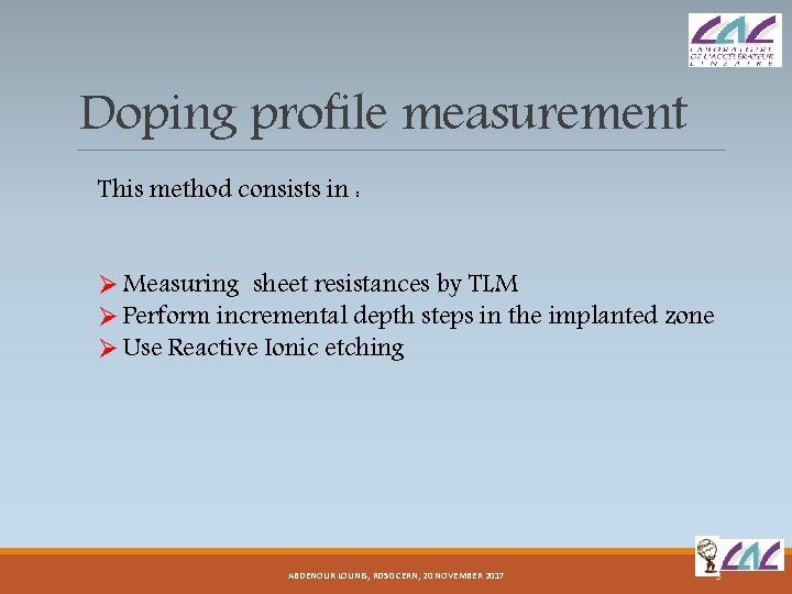
Doping profile measurement This method consists in : Ø Measuring sheet resistances by TLM Ø Perform incremental depth steps in the implanted zone Ø Use Reactive Ionic etching ABDENOUR LOUNIS, RD 50 CERN, 20 NOVEMBER 2017 3

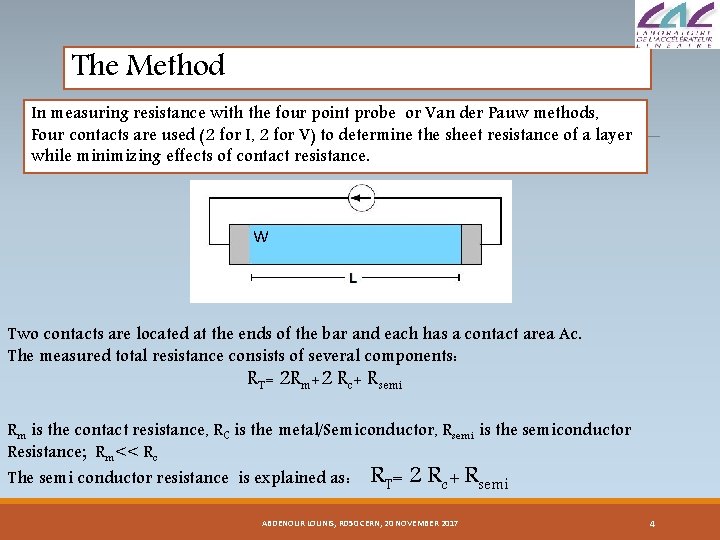
The Method In measuring resistance with the four point probe or Van der Pauw methods, Four contacts are used (2 for I, 2 for V) to determine the sheet resistance of a layer while minimizing effects of contact resistance. W Two contacts are located at the ends of the bar and each has a contact area Ac. The measured total resistance consists of several components: RT= 2 Rm+2 Rc+ Rsemi Rm is the contact resistance, RC is the metal/Semiconductor, Rsemi is the semiconductor Resistance; Rm<< Rc The semi conductor resistance is explained as: RT= 2 Rc+ Rsemi ABDENOUR LOUNIS, RD 50 CERN, 20 NOVEMBER 2017 4

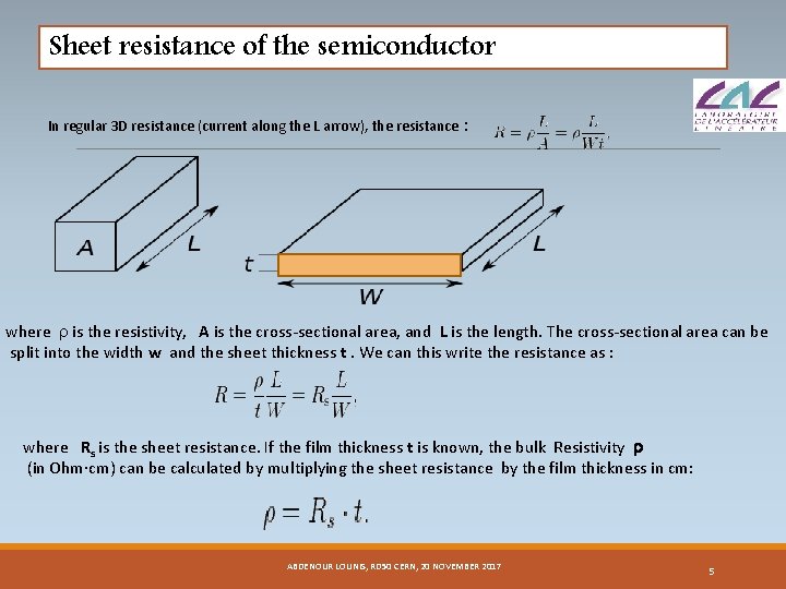
Sheet resistance of the semiconductor In regular 3 D resistance (current along the L arrow), the resistance : where r is the resistivity, A is the cross-sectional area, and L is the length. The cross-sectional area can be split into the width w and the sheet thickness t. We can this write the resistance as : where Rs is the sheet resistance. If the film thickness t is known, the bulk Resistivity r (in Ohm·cm) can be calculated by multiplying the sheet resistance by the film thickness in cm: ABDENOUR LOUNIS, RD 50 CERN, 20 NOVEMBER 2017 5

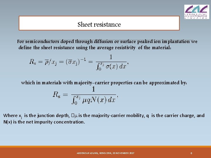
Sheet resistance For semiconductors doped through diffusion or surface peaked ion implantation we define the sheet resistance using the average resistivity of the material: which in materials with majority-carrier properties can be approximated by: Where xj is the junction depth, �m is the majority-carrier mobility, q is the carrier charge, and N(x) is the net impurity concentration. ABDENOUR LOUNIS, RD 50 CERN, 20 NOVEMBER 2017 6

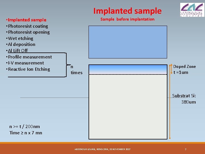
Implanted sample • Photoresist coating • Photoresist opening • Wet etching • Al deposition • Al Lift Off • Profile measurement • I-V measurement • Reactive Ion Etching Sample before implantation n times Doped Zone t =1 um Substrat Si: 380 um n >= t / 200 nm Time ≥ n x 7 mn ABDENOUR LOUNIS, RD 50 CERN, 20 NOVEMBER 2017 7

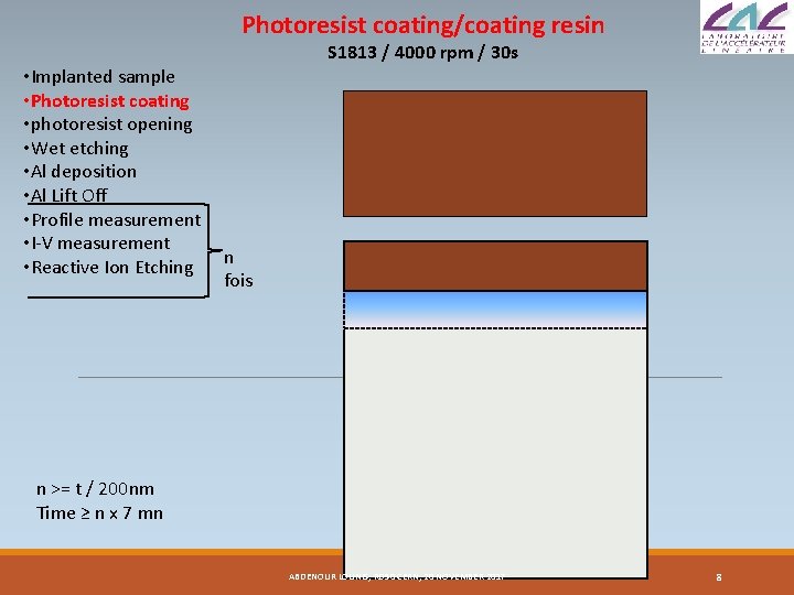
Photoresist coating/coating resin S 1813 / 4000 rpm / 30 s • Implanted sample • Photoresist coating • photoresist opening • Wet etching • Al deposition • Al Lift Off • Profile measurement • I-V measurement • Reactive Ion Etching n fois n >= t / 200 nm Time ≥ n x 7 mn ABDENOUR LOUNIS, RD 50 CERN, 20 NOVEMBER 2017 8

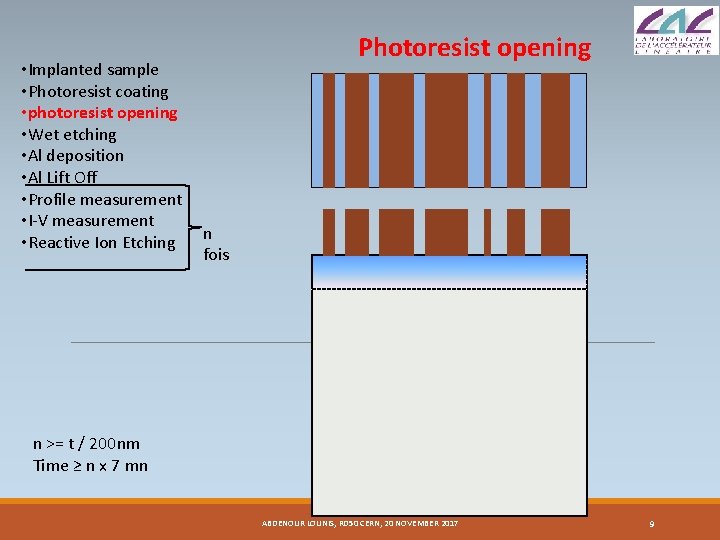
• Implanted sample • Photoresist coating • photoresist opening • Wet etching • Al deposition • Al Lift Off • Profile measurement • I-V measurement • Reactive Ion Etching Photoresist opening n fois n >= t / 200 nm Time ≥ n x 7 mn ABDENOUR LOUNIS, RD 50 CERN, 20 NOVEMBER 2017 9

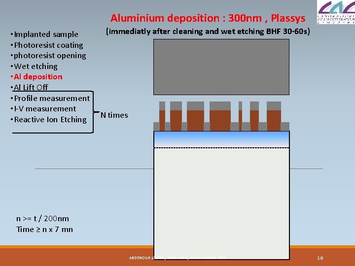
Aluminium deposition : 300 nm , Plassys • Implanted sample • Photoresist coating • photoresist opening • Wet etching • Al deposition • Al Lift Off • Profile measurement • I-V measurement • Reactive Ion Etching (immediatly after cleaning and wet etching BHF 30 -60 s) N times n >= t / 200 nm Time ≥ n x 7 mn ABDENOUR LOUNIS, RD 50 CERN, 20 NOVEMBER 2017 10

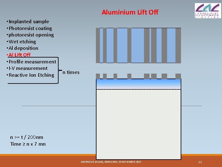
Aluminium Lift Off • Implanted sample • Photoresist coating • photoresist opening • Wet etching • Al deposition • Al Lift Off • Profile measurement • I-V measurement • Reactive Ion Etching n times n >= t / 200 nm Time ≥ n x 7 mn ABDENOUR LOUNIS, RD 50 CERN, 20 NOVEMBER 2017 11

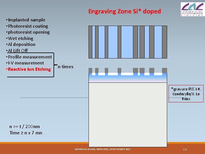
Engraving Zone Si* doped • Implanted sample • Photoresist coating • photoresist opening • Wet etching • Al deposition • Al Lift Off • Profile measurement • I-V measurement • Reactive Ion Etching n times *gravure RIE J-R. Coudevylle/X. Le Roux n >= t / 200 nm Time ≥ n x 7 mn ABDENOUR LOUNIS, RD 50 CERN, 20 NOVEMBER 2017 12

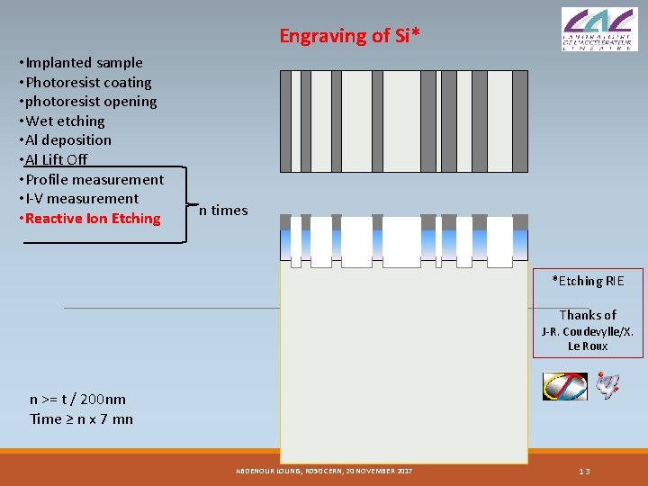
Engraving of Si* • Implanted sample • Photoresist coating • photoresist opening • Wet etching • Al deposition • Al Lift Off • Profile measurement • I-V measurement • Reactive Ion Etching n times *Etching RIE Thanks of J-R. Coudevylle/X. Le Roux n >= t / 200 nm Time ≥ n x 7 mn ABDENOUR LOUNIS, RD 50 CERN, 20 NOVEMBER 2017 13

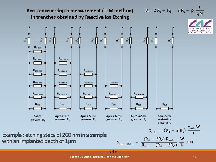
Resistance in-depth measurement (TLM method) in trenches obtained by Reactive Ion Etching Example : etching steps of 200 nm in a sample with an implanted depth of 1µm …. etc. . ABDENOUR LOUNIS, RD 50 CERN, 20 NOVEMBER 2017 14

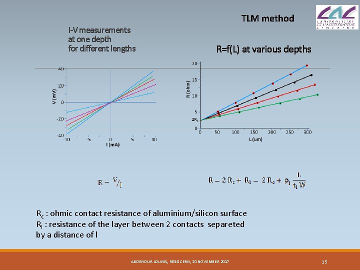
TLM method I-V measurements at one depth for different lengths R=f(L) at various depths Rc : ohmic contact resistance of aluminium/silicon surface Rl : resistance of the layer between 2 contacts separeted by a distance of l ABDENOUR LOUNIS, RD 50 CERN, 20 NOVEMBER 2017 15

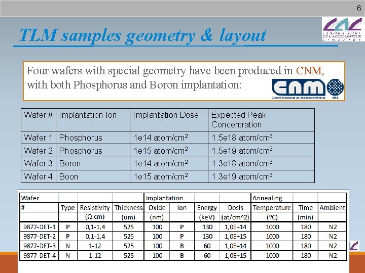
6 TLM samples geometry & layout Four wafers with special geometry have been produced in CNM, with both Phosphorus and Boron implantation: Wafer # Implantation Dose Expected Peak Concentration Wafer 1 Phosphorus 1 e 14 atom/cm 2 1. 5 e 18 atom/cm 3 Wafer 2 Phosphorus 1 e 15 atom/cm 2 1. 5 e 19 atom/cm 3 Wafer 3 Boron 1 e 14 atom/cm 2 1. 3 e 18 atom/cm 3 Wafer 4 Boon 1 e 15 atom/cm 2 1. 3 e 19 atom/cm 3 wafers designed to have similar characteristic to what will be used in ATLAS ITK Upgrade, so that will help to get expectation of real sensors would behave in similar circumstances.

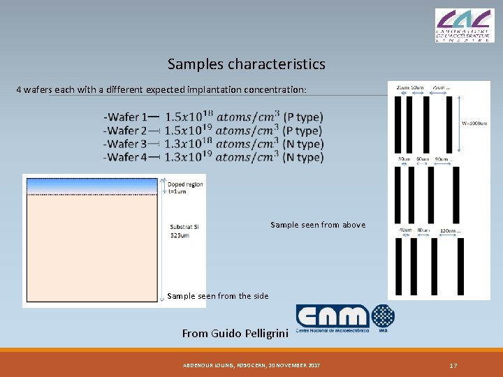
Samples characteristics 4 wafers each with a different expected implantation concentration: Sample seen from above Sample seen from the side From Guido Pelligrini ABDENOUR LOUNIS, RD 50 CERN, 20 NOVEMBER 2017 17

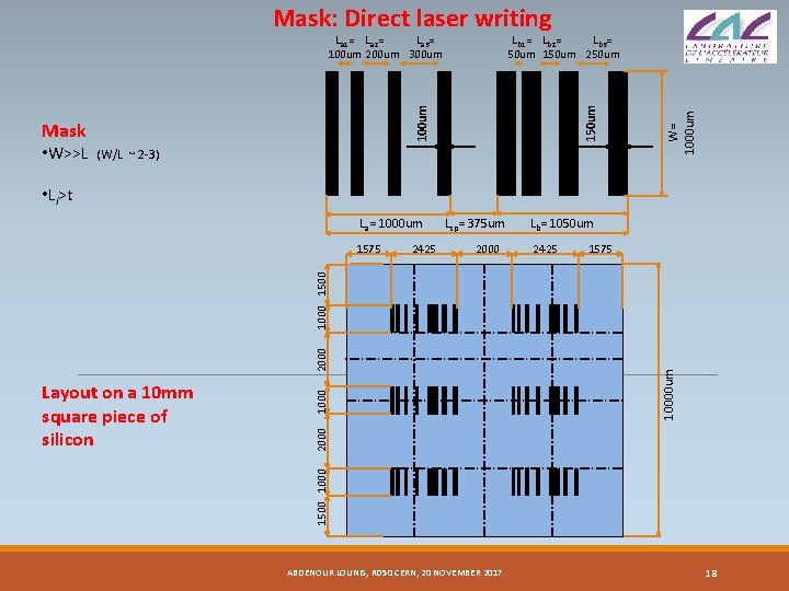
Mask: Direct laser writing (W/L ~ 2 -3) W= 1000 um 150 um Mask • W>>L Lb 1= Lb 2= Lb 3= 50 um 150 um 250 um 100 um La 1= La 2= La 3= 100 um 200 um 300 um • Li>t La= 1000 um 2425 2000 Lb= 1050 um 2425 1575 10000 um 2000 1500 1000 Layout on a 10 mm square piece of silicon 1000 2000 1500 1575 Lsp= 375 um ABDENOUR LOUNIS, RD 50 CERN, 20 NOVEMBER 2017 18

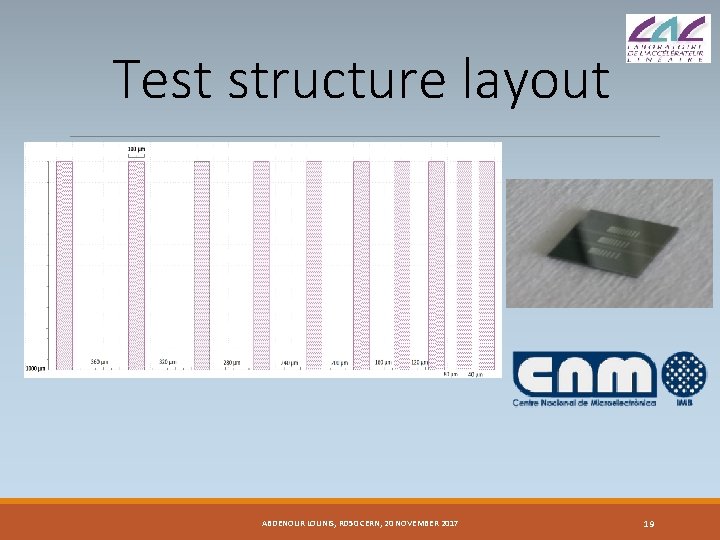
Test structure layout ABDENOUR LOUNIS, RD 50 CERN, 20 NOVEMBER 2017 19

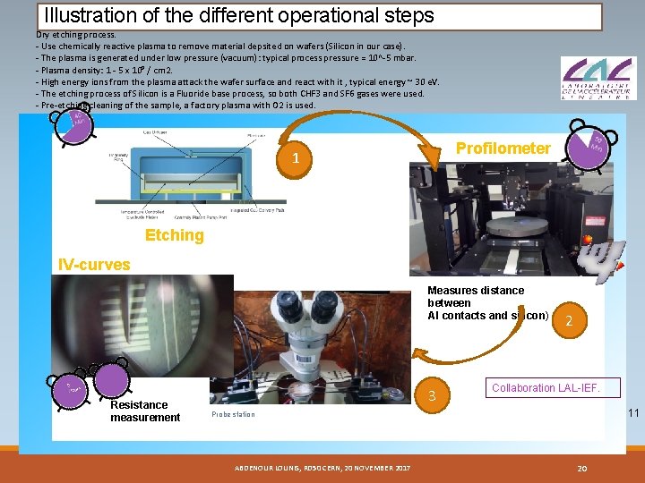
Illustration of the different operational steps Dry etching process. - Use chemically reactive plasma to remove material depsited on wafers (Silicon in our case). - The plasma is generated under low pressure (vacuum): typical process pressure = 10^-5 mbar. - Plasma density: 1 - 5 x 10⁹ / cm 2. - High energy ions from the plasma attack the wafer surface and react with it , typical energy ~ 30 e. V. - The etching process of Silicon is a Fluoride base process, so both CHF 3 and SF 6 gases were used. - Pre-etching cleaning of the sample, a factory plasma with O 2 is used. Profilometer 1 Etching IV-curves Measures distance between Al contacts and silicon) Resistance measurement 3 2 Collaboration LAL-IEF. 11 Probe station ABDENOUR LOUNIS, RD 50 CERN, 20 NOVEMBER 2017 20

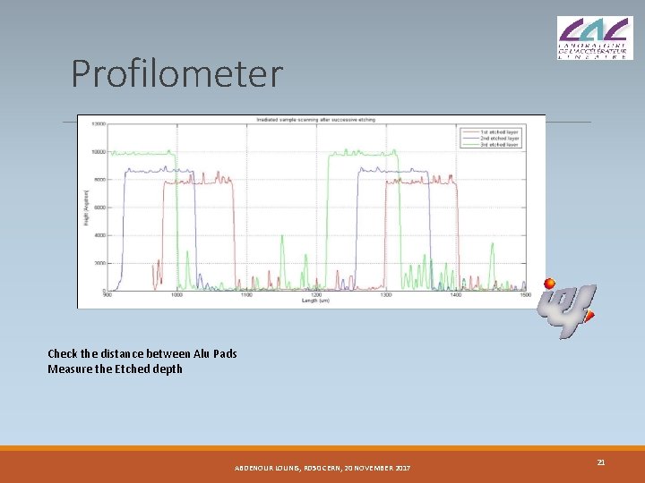
Profilometer Check the distance between Alu Pads Measure the Etched depth ABDENOUR LOUNIS, RD 50 CERN, 20 NOVEMBER 2017 21

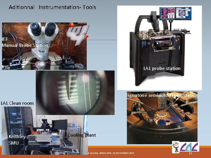
Aditionnal Instrumentation- Tools IEF Manual Probe Station LAL probe station Captinov Signatone semiauto Probe station LAL Clean room Keithley SMU Cooling plant ABDENOUR LOUNIS, RD 50 CERN, 20 NOVEMBER 2017 22

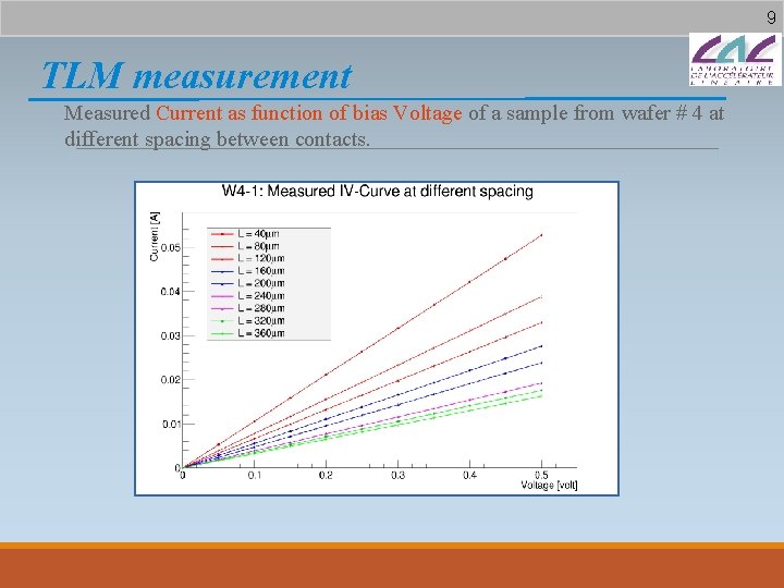
9 TLM measurement Measured Current as function of bias Voltage of a sample from wafer # 4 at different spacing between contacts.

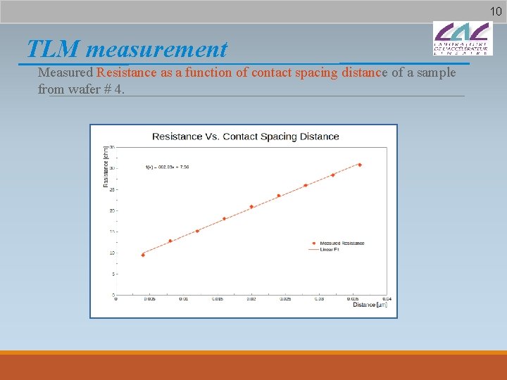
10 TLM measurement Measured Resistance as a function of contact spacing distance of a sample from wafer # 4.

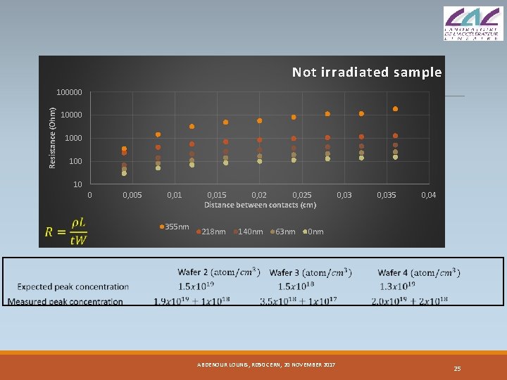
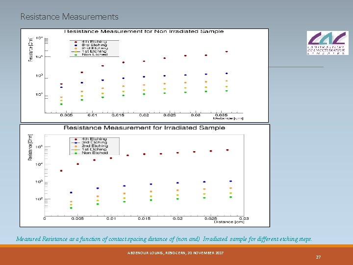
Preliminary results Not irradiated sample Resistance (Ohm) 100000 1000 10 0 0, 005 0, 01 355 nm 0, 015 0, 025 Distance between contacts (cm) 218 nm 140 nm 63 nm 0, 035 0, 04 0 nm ABDENOUR LOUNIS, RD 50 CERN, 20 NOVEMBER 2017 25

Resistance versus contact distance Irradiated sample Resistance (Ohm) 100000 1000 10 0 0, 005 0, 015 0, 02 Distance between contacts (cm) 399 nm 288 nm 197 nm 122 nm 24 nm 0, 025 0, 03 Peak concentration after irradiation could be deduced form the measurements Some TLM samples have been irradiated at Lubjana 2 x 10¹⁵ Neq/cm 2 and 2 x 10¹⁶ ABDENOUR LOUNIS, RD 50 CERN, 20 NOVEMBER 2017 26

Resistance Measurements Measured Resistance as a function of contact spacing distance of (non and) Irradiated sample for different etching steps. ABDENOUR LOUNIS, RD 50 CERN, 20 NOVEMBER 2017 27

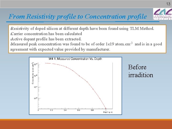
13 From Resistivity profile to Concentration profile Resistivity of doped silicon at different depth have been found using TLM Method. � Carrier concentration has been calculated � Active dopant profile has been extracted. � Measured peak concentration was found to be of order 1 e 19 atom. cm-3 and is in a good agreement with expected value provided by manufacturer. � Before irradition

What is the total doping concentration and how does it compare with Active doping profile? ABDENOUR LOUNIS, RD 50 CERN, 20 NOVEMBER 2017 29

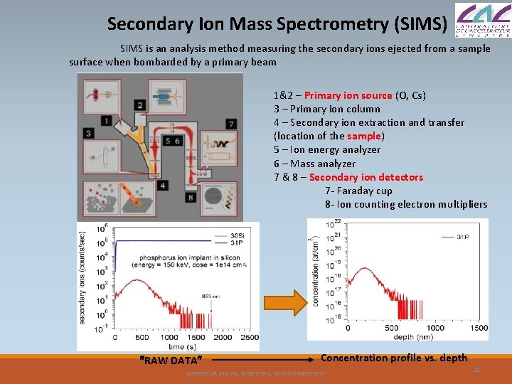
Secondary Ion Mass Spectrometry (SIMS) • General characteristics of sims – Analytical technique to characterize the impurities in the surface and near surface (~30 m) region of solids (e. g. semiconductors) or some liquids; – It relies on the sputtering of a primary energetic ion beam (0. 5 -20 ke. V) on the surface sample and the analysis of the produced ionized secondary particles by mass spectrometry; – It has good detection sensitivity for many elements: it can detect dopant densities as low as 1014 cm-3; – It allows simultaneous detection of different elements, has a depth resolution of 1 to 5 nm and can give a lateral surface characterization on a scale of several microns; – It is a destructive method, since the act of the removing material by sputtering leaves a crater in a sample; – It determines the total dopant density profile and not the electrically active impurity density (e. g. electrical methods as spreading resistance profiling, TLM, Hall effect etc. . ). ABDENOUR LOUNIS, RD 50 CERN, 20 NOVEMBER 2017 30

Secondary Ion Mass Spectrometry (SIMS) SIMS is an analysis method measuring the secondary ions ejected from a sample surface when bombarded by a primary beam 1&2 – Primary ion source (O, Cs) 3 – Primary ion column 4 – Secondary ion extraction and transfer (location of the sample) 5 – Ion energy analyzer 6 – Mass analyzer 7 & 8 – Secondary ion detectors 7 - Faraday cup 8 - Ion counting electron multipliers RAW DATA Concentration profile vs. depth ABDENOUR LOUNIS, RD 50 CERN, 20 NOVEMBER 2017 31

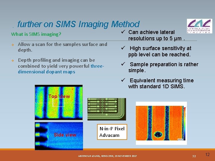
further on SIMS Imaging Method What is SIMS imaging? Allow a scan for the samples surface and depth. Depth profiling and imaging can be combined to yield very powerful threedimensional dopant maps Can achieve lateral resolutions up to 5 µm. High surface sensitivity at ppb level can be reached. Sample preparation is rather simple. Equivalent measuring time with standard 1 D Si. MS. Top View Side view N-in-P Pixel Advacam ABDENOUR LOUNIS, RD 50 CERN, 20 NOVEMBER 2017 32 12

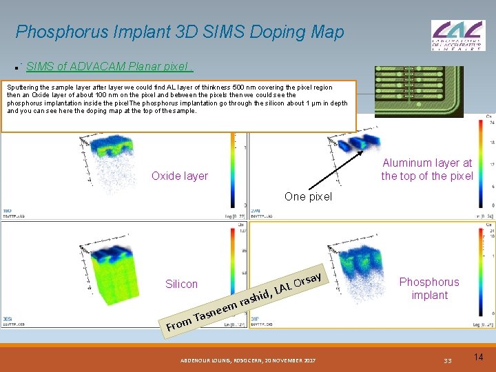
Phosphorus Implant 3 D SIMS Doping Map SIMS of ADVACAM Planar pixel. Sputtering the sample layer after layer we could find AL layer of thinkness 500 nm covering the pixel region then an Oxide layer of about 100 nm on the pixel and between the pixels then we could see the phosphorus implantation inside the pixel. The phosphorus implantation go through the silicon about 1 µm in depth and you can see here the doping map at the top of the sample. Aluminum layer at the top of the pixel Oxide layer One pixel m From y rsa O L A Silicon ee n s a T , L d i h ras ABDENOUR LOUNIS, RD 50 CERN, 20 NOVEMBER 2017 Phosphorus implant 33 14

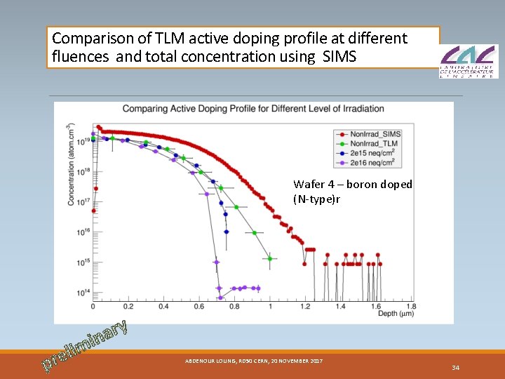
Comparison of TLM active doping profile at different fluences and total concentration using SIMS Wafer 4 – boron doped (N-type)r i l e pr y r a n i m ABDENOUR LOUNIS, RD 50 CERN, 20 NOVEMBER 2017 34

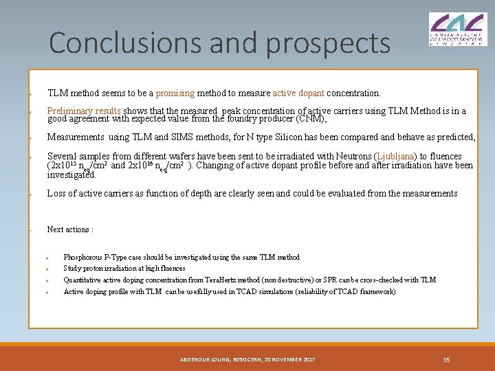
Conclusions and prospects TLM method seems to be a promising method to measure active dopant concentration. Preliminary results shows that the measured peak concentration of active carriers using TLM Method is in a good agreement with expected value from the foundry producer (CNM), Measurements using TLM and SIMS methods, for N type Silicon has been compared and behave as predicted, Several samples from different wafers have been sent to be irradiated with Neutrons (Ljubljana) to fluences (2 x 10¹⁵ neq/cm 2 and 2 x 10¹⁶ neq/cm 2 ). Changing of active dopant profile before and after irradiation have been investigated. Loss of active carriers as function of depth are clearly seen and could be evaluated from the measurements Next actions : v Phosphorous P-Type case should be investigated using the same TLM method v Study proton irradiation at high fluences v Quantitative active doping concentration from Tera. Hertz method (non destructive) or SPR can be cross-checked with TLM v Active doping profile with TLM can be usefully used in TCAD simulations (reliability of TCAD framework) ABDENOUR LOUNIS, RD 50 CERN, 20 NOVEMBER 2017 35

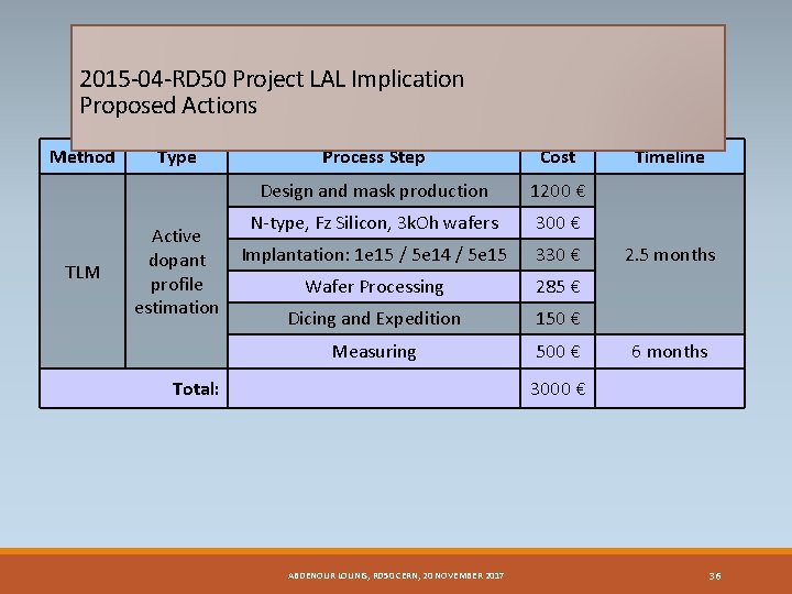
2015 -04 -RD 50 Project LAL Implication Proposed Actions Method TLM Type Active dopant profile estimation Process Step Cost Design and mask production 1200 € N-type, Fz Silicon, 3 k. Oh wafers 300 € Implantation: 1 e 15 / 5 e 14 / 5 e 15 330 € Wafer Processing 285 € Dicing and Expedition 150 € Measuring 500 € Total: Timeline 2. 5 months 6 months 3000 € ABDENOUR LOUNIS, RD 50 CERN, 20 NOVEMBER 2017 36