Active Clamp Forward Reset Technique Using the UCC





- Slides: 26

Active Clamp Forward Reset Technique Using the UCC 2891 PWM Controller Steve Mappus

Agenda u Traditional Transformer Reset Techniques n Third Winding, RCD Clamp, Resonant Reset u Active Clamp Reset Forward Topology n n High Side Clamp Low Side Clamp Timing Diagrams ZVS Design Considerations u Introducing the UCC 2891/2/3/4 n Features, Part Differences, Applications u UCC 2891 EVM n n n Active Clamp Operation and Performance Characteristics Transformer Design Considerations Primary and Secondary Gate Drives ZVS Waveforms Possible Performance Improvements u Reference Materials u UCC 2891 Final Thoughts

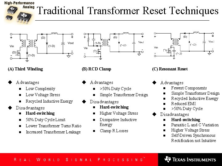
Traditional Transformer Reset Techniques (A) Third Winding (B) RCD Clamp (C) Resonant Reset u Advantages n n n Low Complexity Low Voltage Stress Recycled Inductive Energy u Disadvantages n n Hard-switching 50% Duty Cycle Limit Lower Transformer Turns Ratio Increased Transformer Leakage n n >50% Duty Cycle Simple Transformer Design u Disadvantages n n Hard-switching Higher Voltage Stress Dissipative Inductive Energy Clamp R Losses n n n Fewest Components Simple Transformer Design Recycled Inductive Energy Reduced EMI >50% Duty Cycle u Disadvantages n n Hard-switching Parasitic L and C Variation Higher Voltage Stress Self-Driven Synchronous Rectification not Intuitive

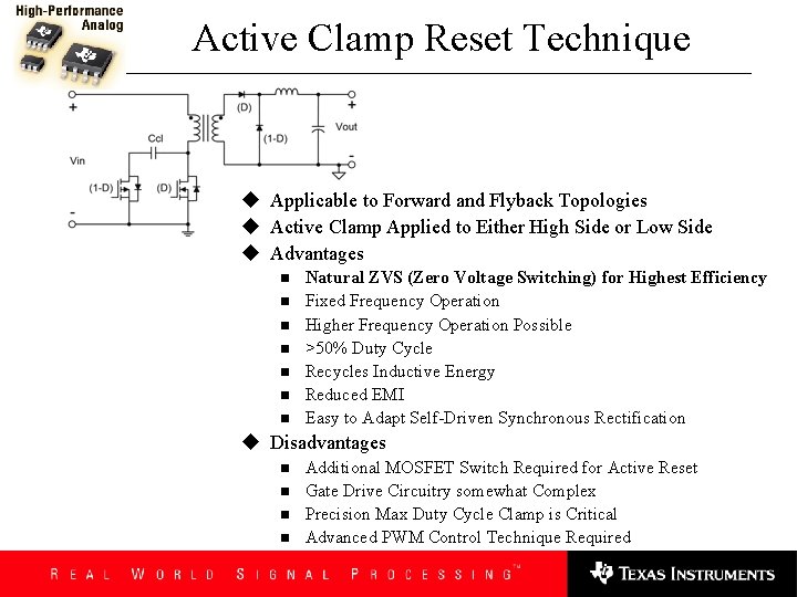
Active Clamp Reset Technique u Applicable to Forward and Flyback Topologies u Active Clamp Applied to Either High Side or Low Side u Advantages n n n n Natural ZVS (Zero Voltage Switching) for Highest Efficiency Fixed Frequency Operation Higher Frequency Operation Possible >50% Duty Cycle Recycles Inductive Energy Reduced EMI Easy to Adapt Self-Driven Synchronous Rectification u Disadvantages n n Additional MOSFET Switch Required for Active Reset Gate Drive Circuitry somewhat Complex Precision Max Duty Cycle Clamp is Critical Advanced PWM Control Technique Required

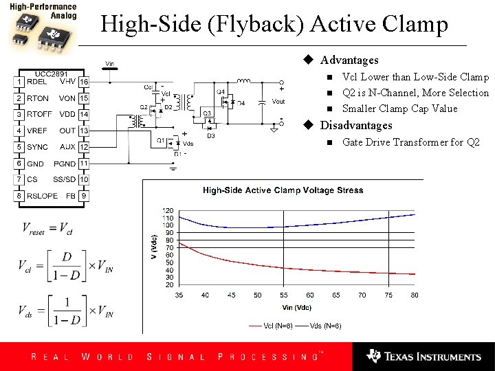
High-Side (Flyback) Active Clamp u Advantages n n n Vcl Lower than Low-Side Clamp Q 2 is N-Channel, More Selection Smaller Clamp Cap Value u Disadvantages n Gate Drive Transformer for Q 2

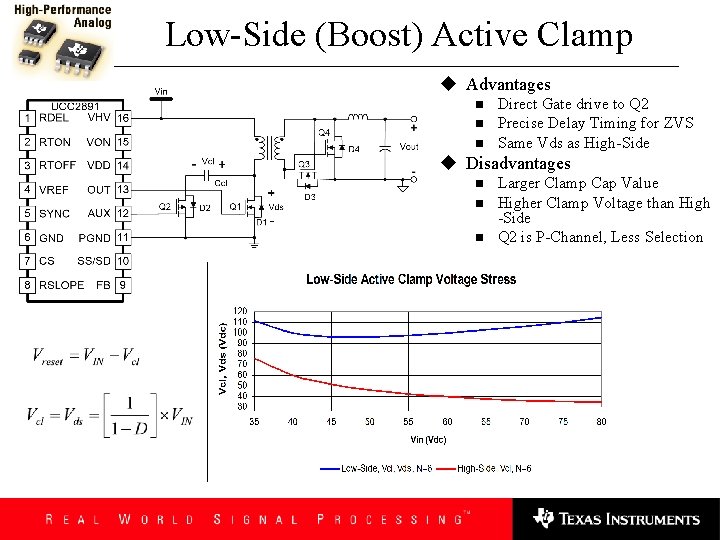
Low-Side (Boost) Active Clamp u Advantages n n n Direct Gate drive to Q 2 Precise Delay Timing for ZVS Same Vds as High-Side u Disadvantages n n n Larger Clamp Cap Value Higher Clamp Voltage than High -Side Q 2 is P-Channel, Less Selection

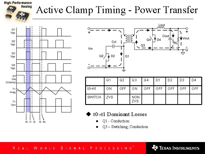
Active Clamp Timing - Power Transfer Q 1 Q 2 Q 3 Q 4 D 1 D 2 D 3 D 4 t 0 t 1 ON OFF OFF OFF SWITCH ZVS NON ZVS u t 0 t 1 Dominant Losses n n Q 1 - Conduction Q 3 – Switching, Conduction

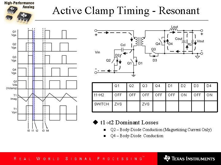
Active Clamp Timing - Resonant Q 1 Q 2 Q 3 Q 4 D 1 D 2 D 3 D 4 t 1 t 2 OFF OFF OFF ON SWITCH ZVS u t 1 t 2 Dominant Losses n n Q 2 – Body-Diode Conduction (Magnetizing Current Only) Q 4 – Body-Diode Conduction

Active Clamp Timing - Clamp t 2 t 3 SWITCH Q 1 Q 2 Q 3 Q 4 D 1 D 2 D 3 D 4 OFF ON OFF OFF ZVS u t 2 t 3 Dominant Losses n n Q 2 – Conduction (Magnetizing Current Only) Q 4 - Conduction

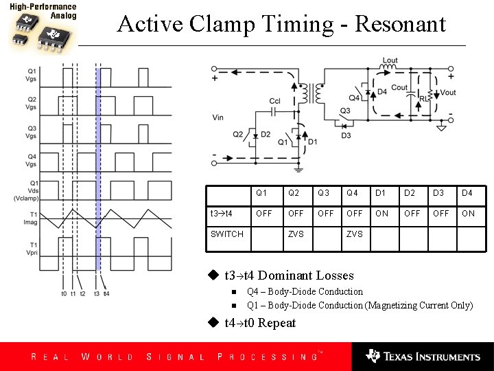
Active Clamp Timing - Resonant t 3 t 4 SWITCH Q 1 Q 2 Q 3 Q 4 D 1 D 2 D 3 D 4 OFF OFF ON ZVS u t 3 t 4 Dominant Losses n n Q 4 – Body-Diode Conduction Q 1 – Body-Diode Conduction (Magnetizing Current Only) u t 4 t 0 Repeat

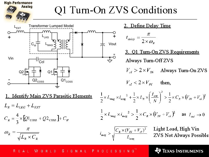
Q 1 Turn-On ZVS Conditions 2. Define Delay Time 3. Q 1 Turn-On ZVS Requirements Always Turn-Off ZVS Always Turn-On ZVS then, 1. Identify Main ZVS Parasitic Elements as Light Load, High Vin ZVS Not Always Possible

Q 1 ZVS Simplified u Resonant Cycle at Q 1 Turn-On n ZVS Achieved if: u Resonant Cycle at Q 1 Turn-Off n n n Within Set Delay Time n n Always Achieve ZVS Resonant Capacitance Naturally Discharges in Same Direction as Resonant Current dominated by IMAG is Peak at Q 1 Turn-Off

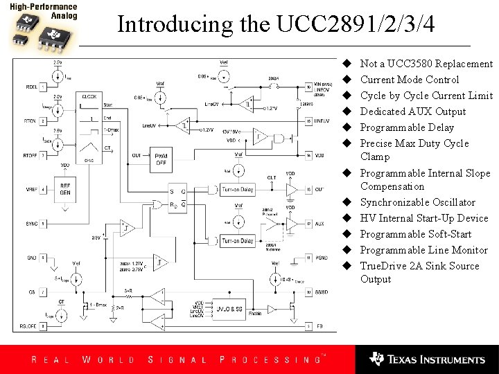
Introducing the UCC 2891/2/3/4 u u u Not a UCC 3580 Replacement Current Mode Control Cycle by Cycle Current Limit Dedicated AUX Output Programmable Delay Precise Max Duty Cycle Clamp Programmable Internal Slope Compensation Synchronizable Oscillator HV Internal Start-Up Device Programmable Soft-Start Programmable Line Monitor True. Drive 2 A Sink Source Output

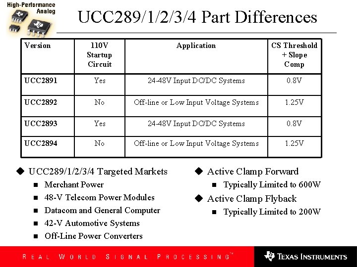
UCC 289/1/2/3/4 Part Differences Version 110 V Startup Circuit Application CS Threshold + Slope Comp UCC 2891 Yes 24 -48 V Input DC/DC Systems 0. 8 V UCC 2892 No Off-line or Low Input Voltage Systems 1. 25 V UCC 2893 Yes 24 -48 V Input DC/DC Systems 0. 8 V UCC 2894 No Off-line or Low Input Voltage Systems 1. 25 V u UCC 289/1/2/3/4 Targeted Markets n n n Merchant Power 48 -V Telecom Power Modules Datacom and General Computer 42 -V Automotive Systems Off-Line Power Converters u Active Clamp Forward n Typically Limited to 600 W u Active Clamp Flyback n Typically Limited to 200 W

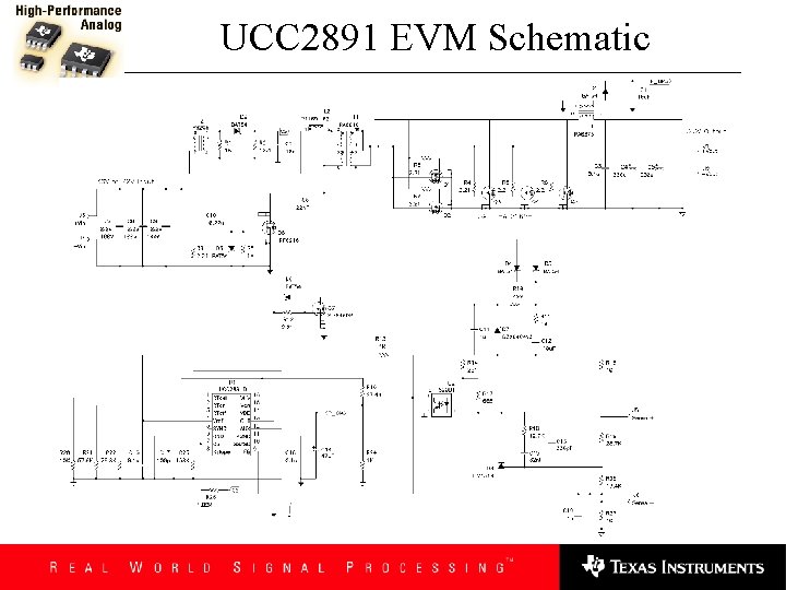
UCC 2891 EVM u EVM Features n n n n 100 W Half Brick Active Clamp Forward Self-Driven Synchronous Rectification ZVS High Efficiency Very Low Component Count Low Input Line Monitor Output Short Circuit Protection Regulates to Zero Load u Specifications n n n 36 V < VIN < 75 V 0 A < IOUT < 30 A VO = 3. 3 V 1% FS = 300 k. Hz Line Reg < 0. 1% Load Reg < 0. 1%

UCC 2891 EVM Schematic

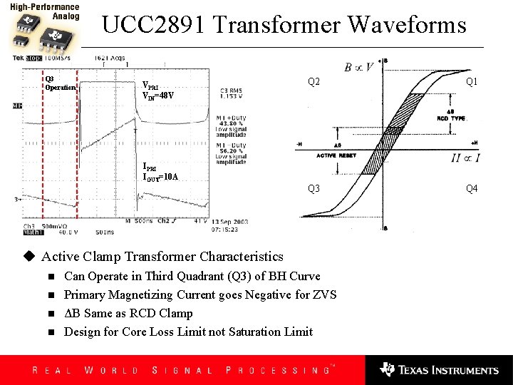
UCC 2891 Transformer Waveforms Q 3 Operation VPRI VIN=48 V Q 2 Q 1 Q 3 Q 4 IPRI IOUT=10 A u Active Clamp Transformer Characteristics n n Can Operate in Third Quadrant (Q 3) of BH Curve Primary Magnetizing Current goes Negative for ZVS ΔB Same as RCD Clamp Design for Core Loss Limit not Saturation Limit

UCC 2891 EVM Clamp Voltage Limits VGS VCL IPRI u Vin=36 V, Iout=10 A n n Dmax=58% Vclamp=89 V u Vin=72 V, Iout=10 A n n Dmin=28% Vclamp=102 V

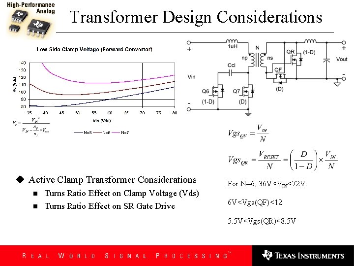
Transformer Design Considerations u Active Clamp Transformer Considerations n n Turns Ratio Effect on Clamp Voltage (Vds) Turns Ratio Effect on SR Gate Drive For N=6, 36 V<VIN<72 V: 6 V<Vgs(QF)<12 5. 5 V<Vgs(QR)<8. 5 V

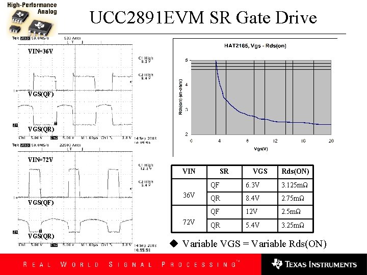
UCC 2891 EVM SR Gate Drive VIN=36 V VGS(QF) VGS(QR) VIN=72 V VIN VGS(QF) 36 V 72 V VGS(QR) SR VGS Rds(ON) QF 6. 3 V 3. 125 mΩ QR 8. 4 V 2. 75 mΩ QF 12 V 2. 5 mΩ QR 5. 4 V 3. 25 mΩ u Variable VGS = Variable Rds(ON)

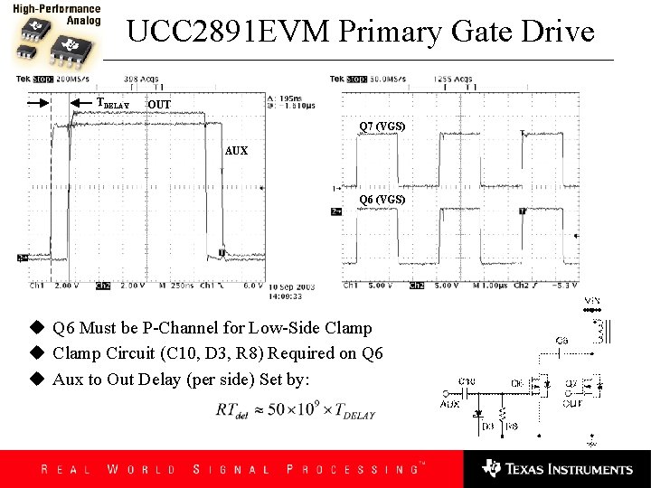
UCC 2891 EVM Primary Gate Drive TDELAY OUT Q 7 (VGS) AUX Q 6 (VGS) u Q 6 Must be P-Channel for Low-Side Clamp u Clamp Circuit (C 10, D 3, R 8) Required on Q 6 u Aux to Out Delay (per side) Set by:

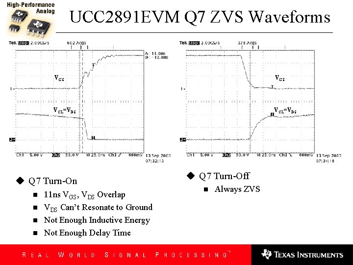
UCC 2891 EVM Q 7 ZVS Waveforms VGS VCL=VDS u Q 7 Turn-On n n 11 ns VGS, VDS Overlap VDS Can’t Resonate to Ground Not Enough Inductive Energy Not Enough Delay Time u Q 7 Turn-Off n Always ZVS

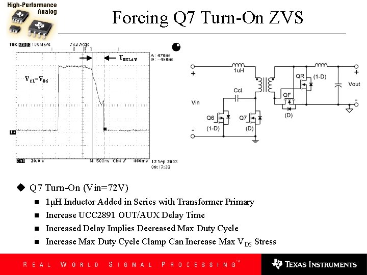
Forcing Q 7 Turn-On ZVS TDELAY VCL=VDS u Q 7 Turn-On (Vin=72 V) n n 1μH Inductor Added in Series with Transformer Primary Increase UCC 2891 OUT/AUX Delay Time Increased Delay Implies Decreased Max Duty Cycle Increase Max Duty Cycle Clamp Can Increase Max VDS Stress

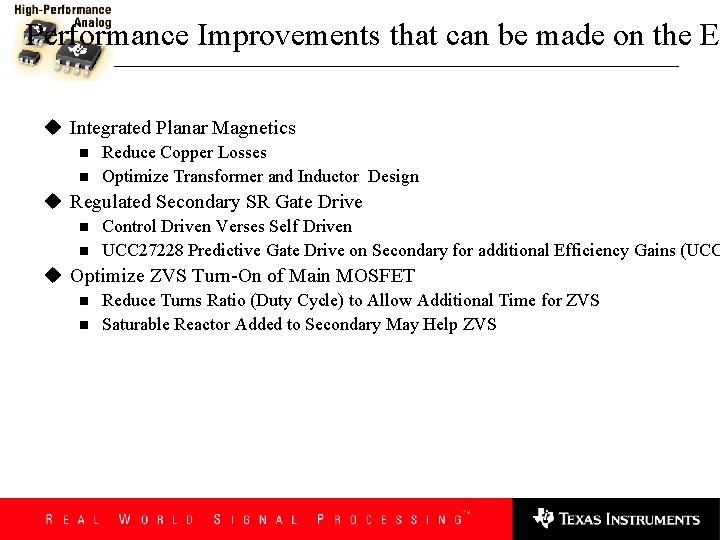
Performance Improvements that can be made on the E u Integrated Planar Magnetics n n Reduce Copper Losses Optimize Transformer and Inductor Design u Regulated Secondary SR Gate Drive n n Control Driven Verses Self Driven UCC 27228 Predictive Gate Drive on Secondary for additional Efficiency Gains (UCC u Optimize ZVS Turn-On of Main MOSFET n n Reduce Turns Ratio (Duty Cycle) to Allow Additional Time for ZVS Saturable Reactor Added to Secondary May Help ZVS

References Literature u u u UCC 289/1/2/3/4 Current-Mode Active Clamp PWM Controller Datasheet, Texas Instruments Lite Active Clamp and Reset Technique Enhances Forward Converter Performance, Power Supply Design Considerations for Active Clamp and Reset Technique, Power Supply Design Seminar SEM 48 -V Input, 3. 3 V/100 Watt Converter With UCC 3580 -1 Controller, User guide to Accommodate P UCC 2891 EVM, 48 -V to 1. 3 -V, 30 -A Forward Converter with Active Clamp Reset, User Guide to A Designing for High Efficiency with the UCC 289/1/2/3/4 Active Clamp PWM Controller, Applicatio Development Tools u UCC 2891 EVM, 48 -V to 3. 3 -V, 30 -A Forward Converter with Active Clamp Reset, Texas Instrume

UCC 2891 Final Thoughts u Part Differences n n UCC 2891/3 for 24 -48 V isolated input systems UCC 2892/4 for Off-Line Applications or low input voltage systems below 24 Vin u ZVS n n Always Get ZVS at Turn-Off Conditional ZVS at Turn-On u UCC 2891 Highlights n n n High Efficiency Loaded With Internal Part Features Improved Performance and Features over Competition ± 2 A True. Drive™ Output Stage 2891 Eliminates the “Disadvantages” Normally Associated with Active Clamp u Product Released October 30, 2003