ACOE 201 Computer Architecture I Laboratory Exercises Background
ACOE 201 – Computer Architecture I – Laboratory Exercises Background and Introduction to FPGAs Dr. Konstantinos Tatas com. tk@fit. ac. cy http: //staff. fit. ac. cy/com. tk
ACOE 201 Laboratory Structure and Objectives • Small group experiments lasting approximately two periods • Lab report • Design and implementation of a simple CPU • Hardware: Xilinx Spartan-3 E Starter Kit • Software: Xilinx ISE • Objectives: – Develop practical digital design skills – Reinforce Computer Architecture concepts by designing and verifying a simple CPU
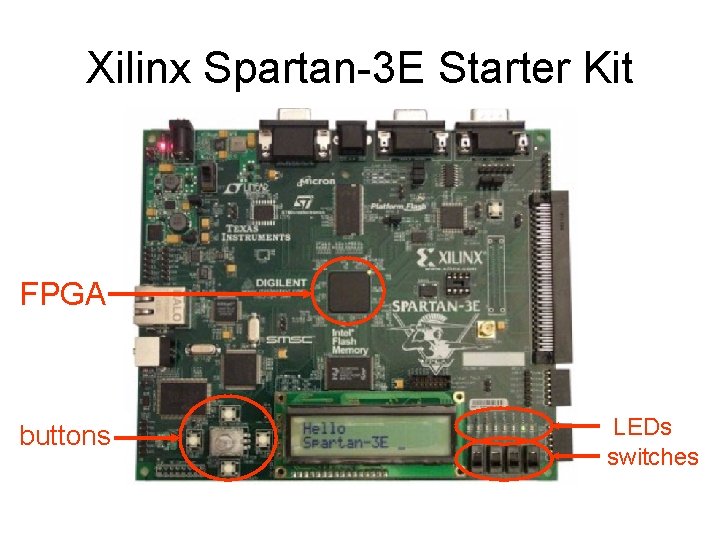
Xilinx Spartan-3 E Starter Kit FPGA buttons LEDs switches
FPGA Principles • A Field-Programmable Gate Array (FPGA) is an integrated circuit that can be configured by the user to emulate any digital circuit as long as there are enough resources • An FPGA can be seen as an array of Configurable Logic Blocks (CLBs) connected through programmable interconnect (Switch Boxes)
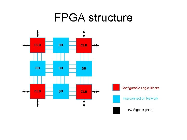
FPGA structure
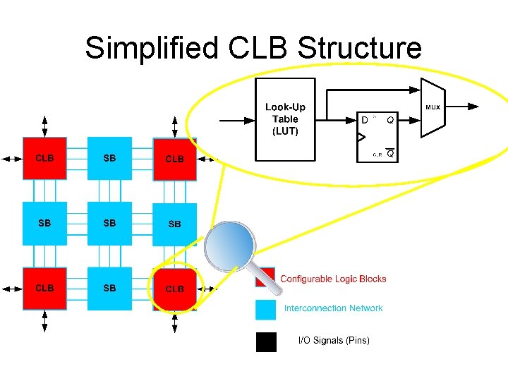
Simplified CLB Structure
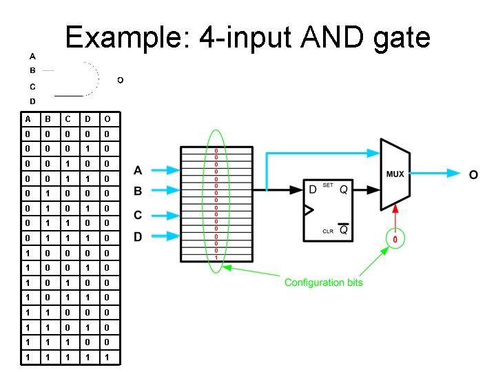
Example: 4 -input AND gate A B C D O 0 0 0 0 1 1 0 0 0 0 1 1 0 0 0 1 1 1 0 0 0 0 1 0 1 0 0 1 1 0 0 0 1 1 1 0 0 1 1 1
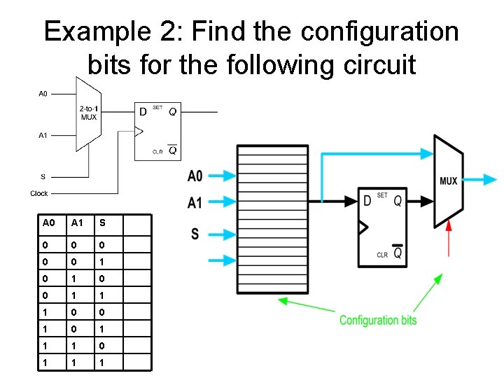
Example 2: Find the configuration bits for the following circuit A 0 A 1 S 0 0 0 1 1 1 0 0 1 1 1
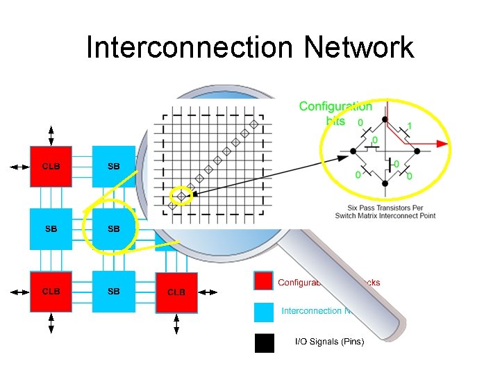
Interconnection Network
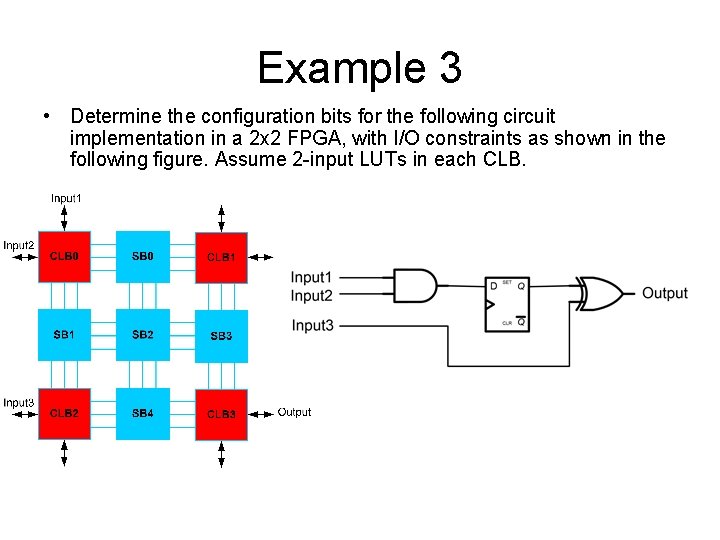
Example 3 • Determine the configuration bits for the following circuit implementation in a 2 x 2 FPGA, with I/O constraints as shown in the following figure. Assume 2 -input LUTs in each CLB.
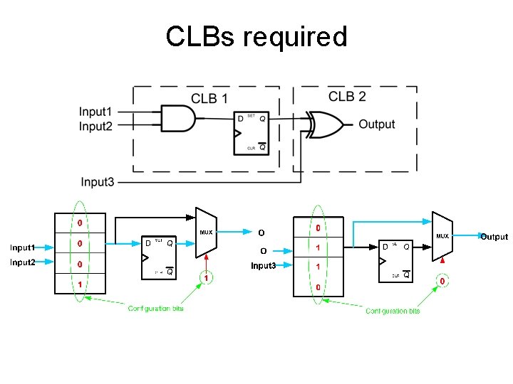
CLBs required
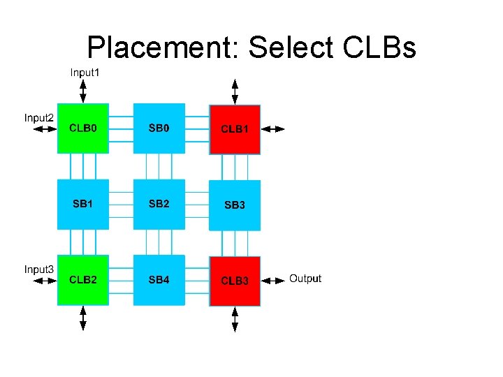
Placement: Select CLBs
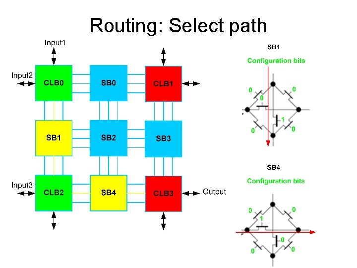
Routing: Select path
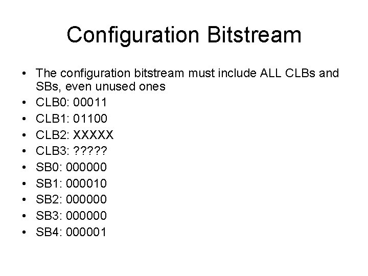
Configuration Bitstream • The configuration bitstream must include ALL CLBs and SBs, even unused ones • CLB 0: 00011 • CLB 1: 01100 • CLB 2: XXXXX • CLB 3: ? ? ? • SB 0: 000000 • SB 1: 000010 • SB 2: 000000 • SB 3: 000000 • SB 4: 000001
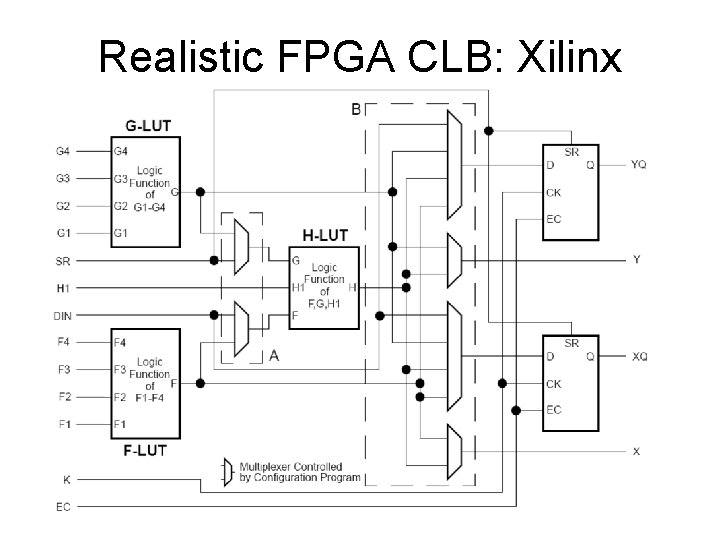
Realistic FPGA CLB: Xilinx
FPGA EDA Tools • Must provide a design environment based on digital design concepts and components (gates, flip-flops, MUXs, etc. ) • Must hide the complexities of placement, routing and bitstream generation from the user. Manual placement, routing and bitstream generation is infeasible for practical FPGA array sizes and circuit complexities.
- Slides: 16