
Access to 65 nm Technology through CERN Sandro
- Slides: 11
Access to 65 nm Technology through CERN Sandro Bonacini, Kostas Kloukinas, Alessandro Marchioro, CERN, PH-ESE dept. CH 1211, Geneve 23 Switzerland
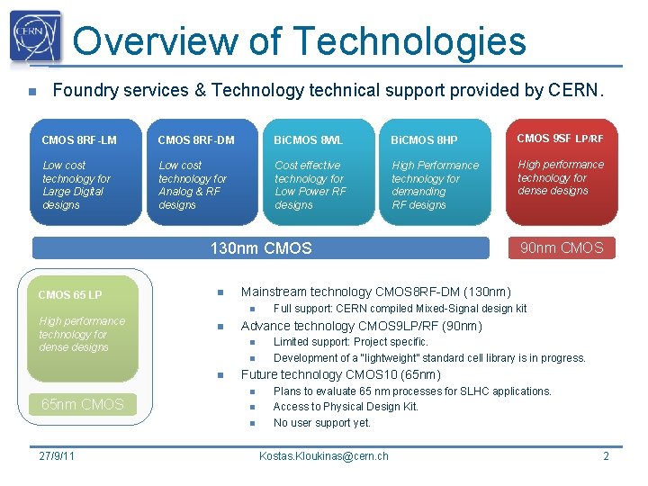
Overview of Technologies n Foundry services & Technology technical support provided by CERN. CMOS 8 RF-LM CMOS 8 RF-DM Bi. CMOS 8 WL Bi. CMOS 8 HP CMOS 9 SF LP/RF Low cost technology for Large Digital designs Low cost technology for Analog & RF designs Cost effective technology for Low Power RF designs High Performance technology for demanding RF designs High performance technology for dense designs 130 nm CMOS 65 LP n Mainstream technology CMOS 8 RF-DM (130 nm) n High performance technology for dense designs n n 27/9/11 Limited support: Project specific. Development of a “lightweight” standard cell library is in progress. Future technology CMOS 10 (65 nm) n 65 nm CMOS Full support: CERN compiled Mixed-Signal design kit Advance technology CMOS 9 LP/RF (90 nm) n n 90 nm CMOS Plans to evaluate 65 nm processes for SLHC applications. Access to Physical Design Kit. No user support yet. Kostas. Kloukinas@cern. ch 2
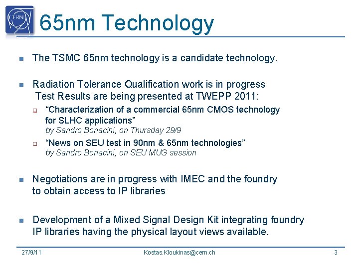
65 nm Technology n The TSMC 65 nm technology is a candidate technology. n Radiation Tolerance Qualification work is in progress Test Results are being presented at TWEPP 2011: q “Characterization of a commercial 65 nm CMOS technology for SLHC applications” by Sandro Bonacini, on Thursday 29/9 q “News on SEU test in 90 nm & 65 nm technologies” by Sandro Bonacini, on SEU MUG session n Negotiations are in progress with IMEC and the foundry to obtain access to IP libraries n Development of a Mixed Signal Design Kit integrating foundry IP libraries having the physical layout views available. 27/9/11 Kostas. Kloukinas@cern. ch 3
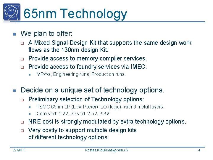
65 nm Technology n We plan to offer: q q q A Mixed Signal Design Kit that supports the same design work flows as the 130 nm design Kit. Provide access to memory compiler services. Provide access to foundry services via IMEC. n n MPWs, Engineering runs, Production runs. Decide on a unique set of technology options. q Preliminary selection of Technology options: n n q q 27/9/11 TSMC 65 nm LP (Low Power), LO (logic), with 6 metal layers. Core vdd: 1. 2 V, IO vdd: 2. 5 V, 3. 3 V NRE cost is strongly modulated by extra technology options. Very costly to support multiple design kits of different technology options. Kostas. Kloukinas@cern. ch 4
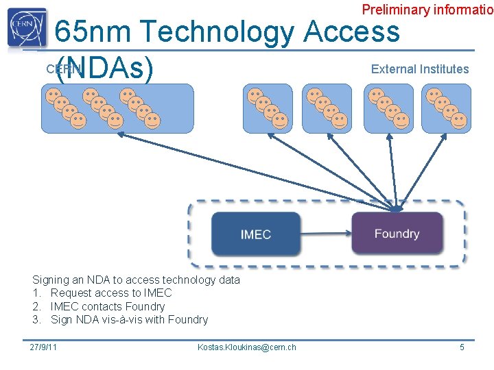
Preliminary informatio 65 nm Technology Access CERN External Institutes (NDAs) Signing an NDA to access technology data 1. Request access to IMEC 2. IMEC contacts Foundry 3. Sign NDA vis-à-vis with Foundry 27/9/11 Kostas. Kloukinas@cern. ch 5
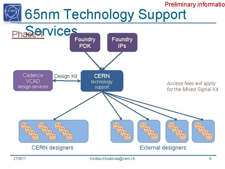
Preliminary informatio 65 nm Technology Support Services Phase 1 Foundry PDK Cadence VCAD Design Kit design services IPs CERN technology support CERN designers 27/9/11 Access fees will apply for the Mixed Signal Kit External designers Kostas. Kloukinas@cern. ch 6
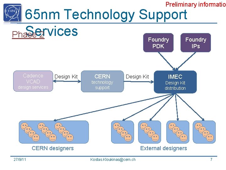
Preliminary informatio 65 nm Technology Support Services Phase 2 Foundry PDK Cadence VCAD Design Kit design services CERN Design Kit technology support CERN designers 27/9/11 IPs IMEC Design Kit distribution External designers Kostas. Kloukinas@cern. ch 7
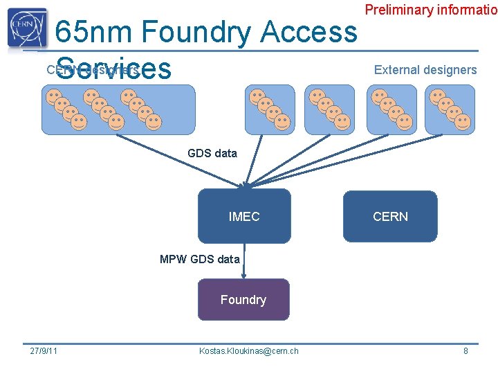
65 nm Foundry Access CERN designers Services Preliminary informatio External designers GDS data IMEC CERN MPW GDS data Foundry 27/9/11 Kostas. Kloukinas@cern. ch 8
THANK YOU One more slide 27/9/11 Kostas. Kloukinas@cern. ch 9
MPW Call for Interest n Please contact for participation to: q Forthcoming MPW runs: n CMOS 8 RF (130 nm) q CERN MPW, February 2012 (tentative) q MOSIS MPW, Nov. 7, 2011 n CMOS 6 (250 nm) q November 2011. n Keep us informed for your future submission plans. n Contact: kostas. kloukinas@cern. ch 27/9/11 Kostas. Kloukinas@cern. ch 10
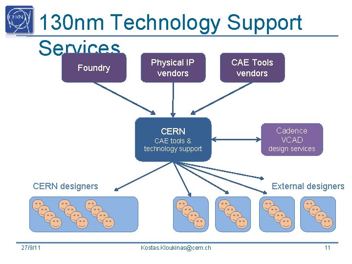
130 nm Technology Support Services Physical IP CAE Tools Foundry vendors CERN CAE tools & technology support CERN designers 27/9/11 vendors Cadence VCAD design services External designers Kostas. Kloukinas@cern. ch 11