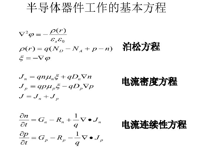
acceptor donor recombination majority minority transition region depletion

acceptor 受主 donor 施主 recombination 复合 majority 多子 minority 少子 transition region 过渡区 depletion region 耗尽区 contact barrier 接触势垒 p-n junction pn结 heterojunction/异质结 EHP 电子空穴对 homojunction/同质结

Schottky barrier /肖特基势垒 barrier height/势垒高度 ideal/理想的 work function/功函数 practical/实际的 electron affinity/电子亲和能 Fermi level/费米能级 electrostatic potential/静电势 rectifier /整流器 breakdown /击穿 rectifying contacts/整流接触 Ohmic contacts/欧姆接触 lattice-matched/晶格匹配的 tunneling effect/隧道效应 surface state/表面态
 Many of the useful properties of a p-n")
5. 7 Metal-Semiconductor junctions or contacts(金属-半导体结、金-半接触) Many of the useful properties of a p-n junction can be achieved by simply forming an appropriate metal-semiconductor(MS) contact.

5. 7. 1 Schottky Barriers • http: //en. wikipedia. org/wiki/Walter_H. _Schottky 1. Schottky effect Possibly, in retrospect, Schottky's most important scientific achievement was to develop (in 1914) the well-known classical formula, now written -q 2/4πε 0 x, for the interaction energy between a point charge q and a flat metal surface, when the charge is at a distance x from the surface. Owing to the method of its derivation, this interaction is called the "image potential energy" (image PE). Schottky based his work on earlier work by (Lord) Kelvin relating to the image PE for a sphere. Schottky's image PE has become a standard component in simple models of the barrier to motion, M(x), experienced by an electron on approaching a metal surface or a metal-semiconductor interface from the inside.

• (The image PE is usually combined with terms relating to an applied electric field F and to the height h (in the absence of any field) of the barrier. This leads to the following expression for the dependence of the barrier energy on distance x, measured from the "electrical surface" of the metal, into the vacuum or into the semiconductor: – • Here, e is the elementary positive charge, ε 0 is the electric constant and εr is the relative permittivity of the second medium (=1 for vacuum). In the case of a metal-semiconductor junction, this is called a Schottky barrier; in the case of the metal-vacuum interface, this is sometimes called a Schottky-Nordheim barrier. In many contexts, h has to be taken equal to the local work function φ. • This Schottky-Nordheim barrier (SN barrier) has played in important role in theories of thermionic emission and of field electron emission. Applying the field causes lowering of the barrier, and thus enhances the emission current in thermionic emission. This is called the "Schottky effect", and the resulting emission regime is called "Schottky emission".
: The energy with the work function is required to")
• The work function(功函数): The energy with the work function is required to remove an electron at the Fermi level to the vacuum outside the metal. (Al=4. 3 e. V) • the electron affinity(电 子 亲 和 能 ): The energy with the electron affinity is required to remove an electron at the bottom of the conduction band to the vacuum outside the semiconductors. (Si=4. 1 e. V)
metal-n type semiconductor, q m> q s")
• Four sets of combination: • (1)metal-n type semiconductor, q m> q s • (2)metal-n type semiconductor, q m< q s • (3)metal-p type semiconductor, q m> q s • (4)metal-p type semiconductor, q m< q s

• Two kinds of MS contacts will occur: rectifying and ohmic • The rectifying contact is similar to the p -n junction in function. (diode) • The ohmic contact is usually used to connect semiconductors to electrodes or wires. (resistor)
 (1)q m>q s Metal/n-type semiconductor charge transfer occurs until the Fermi")
2. Schottky barriers(肖特基势垒) (1)q m>q s Metal/n-type semiconductor charge transfer occurs until the Fermi levels align at equilibrium

p the electrostatic potential of the semiconductor must be raised V 0 p the electron energy must be lowered. –q. V 0 p the depletion region is formed near the Φ is called Schottky B junction. p Contact potential barrier: q. V 0=q m-q s p potential barrier height q B= q m-q barrier
Metal/p type semiconductor, q m<q s p. Electrons flow from metal to semiconductor till")
(2)Metal/p type semiconductor, q m<q s p. Electrons flow from metal to semiconductor till the Fermi levels align at equilibrium p the electrostatic potential of the semiconductor must be lowered V 0 p the electron energy must be raised –q. V 0 p the depletion region is formed near the junction. p Contact potential barrier: q. V 0=q s-q m V 0 retards hole diffusion from the semiconductor to the metal
 You can treat the Schottky barrier for M/n-type S")
5. 7. 2 Rectifying contacts(diode) You can treat the Schottky barrier for M/n-type S (or M/ptype S) as the P+N (or N+P)junction except that no hole injection occurs from the metal into the semiconductor. Case 1: Metal-n type contact (a)Forward bias Electrons flow from semiconductor to Metal under forward bias.
Reverse bias How about p-n junction? One important feature is that the saturation current")
(b)Reverse bias How about p-n junction? One important feature is that the saturation current I 0 depends upon B and is unaffected by the bias voltage. I 0∝Exp(-q B /k. T)

• For pn junction : ~10 -11 A/cm 2 • For M-S junction
Forward bias Holes flow from semiconductor to metal")
Case 2: metal-p type Schottky contact? (a)Forward bias Holes flow from semiconductor to metal under forward bias. (b)Reverse bias A reverse voltage increases the barrier for hole flow and the current becomes negligible.
 In many cases we wish to have an")
5. 7. 3 Ohmic contacts(ideal, resistor) In many cases we wish to have an ohmic metal-semiconductor contact, having a linear I-V characteristic in both biasing directions. For example, the interconnected lines (互连线)are required in IC. So, it is important that such contacts be ohmic, with minimal resistance and no tendency to rectify signals. The barrier to electron flow between the metal and semiconductor is small and easily overcome by a small voltage. R Case 1 M/n type, qΦm<q Φs

Case 2: metal-p type semiconductor, q m> q s Unlike the rectifying contacts, no depletion region occurs in the semiconductor in these two cases since the electrostatic potential difference required to align the Fermi level at equilibrium calls for accumulation of majority carriers in the semiconductor.
 In practice, it is always impossible for us to")
5. 7. 3 Ohmic contacts(practical) In practice, it is always impossible for us to form the ohmic contacts of metal-semiconductor by choosing the appropriate work function of the metal. The reason is that the semiconductor surface contains surface states due to incomplete covalent bonds. The metal/semiconductor contacts form always a barrier whatever metals are used. So, to obtain the ohmic contacts for metal/semiconductor, a practical method is by doping the semiconductor heavily in the contact regions. Therefore, if a barrier exists at the interface, the depletion width is small enough to allow carriers to tunnel through the barrier. Tunneling probability can be referred to< semiconductor physics>(P 236 -238).
: because of surface states and")
5. 7. 4 Typical Schottky Barriers Pinning effect (钉扎效应): because of surface states and interfacial layer

– P 168 It is easier to obtain the width of the depletion region at M-S Schottky junction. For p-n junction

For M-n type Schottky barrier For M-p type Schottky barrier

PROBLEM 1 • What is the difference between p-n diode and Schottky barrier diode?

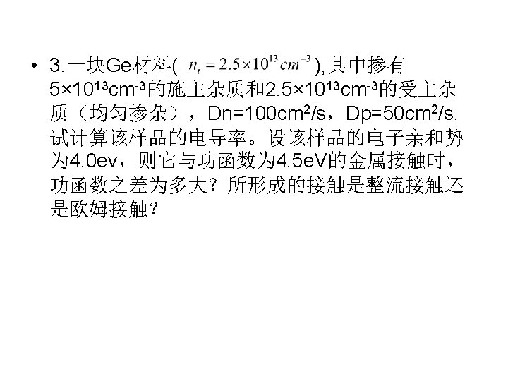
Problem 2 • A Schottky barrier is formed between a metal having a work function of 4. 3 ev and p type Si(electron affinity is 4 ev). The acceptor doping in the Silicon is 1017 cm-3. (a)Calculate q. V 0 and draw the equilibrium band diagram. (b)Draw the band diagram with 0. 3 V forward bias and 2 V reverse bias.
- Slides: 25