Accelerating DSP Algorithms Using FPGAs Sean Gallagher DSP
- Slides: 28

Accelerating DSP Algorithms Using FPGAs Sean Gallagher DSP Specialist Xilinx Inc Gallagher 1 P 188/MAPLD 2004

Why DSP in FPGAs • Availability of fast analog-to-digital converters (ADCs) – Enables digital methods for functions traditionally done in RF components • Massive parallel processing – FPGAs may have several hundred embedded multipliers on-chip – One FPGA can replace many DSP Processors Gallagher 2 P 188/MAPLD 2004

Architectural Considerations • FPGA architectures are vendor specific – Unlike ASICS, no two are alike • FPGA vendors develop distinct competencies – In device architecture design – In intellectual property (dsp functions, bus controllers, etc) – In design tool flows • Vendor independent HDL can be written but this usually achieves mediocre results in clock speed and design size instantiation Gallagher 3 P 188/MAPLD 2004

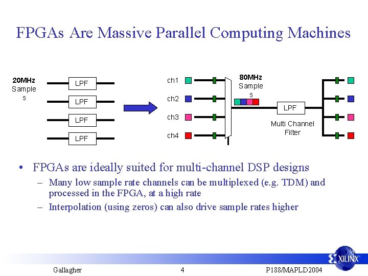
FPGAs Are Massive Parallel Computing Machines 20 MHz Sample s LPF ch 1 LPF ch 2 LPF ch 3 LPF ch 4 80 MHz Sample s LPF Multi Channel Filter • FPGAs are ideally suited for multi-channel DSP designs – Many low sample rate channels can be multiplexed (e. g. TDM) and processed in the FPGA, at a high rate – Interpolation (using zeros) can also drive sample rates higher Gallagher 4 P 188/MAPLD 2004

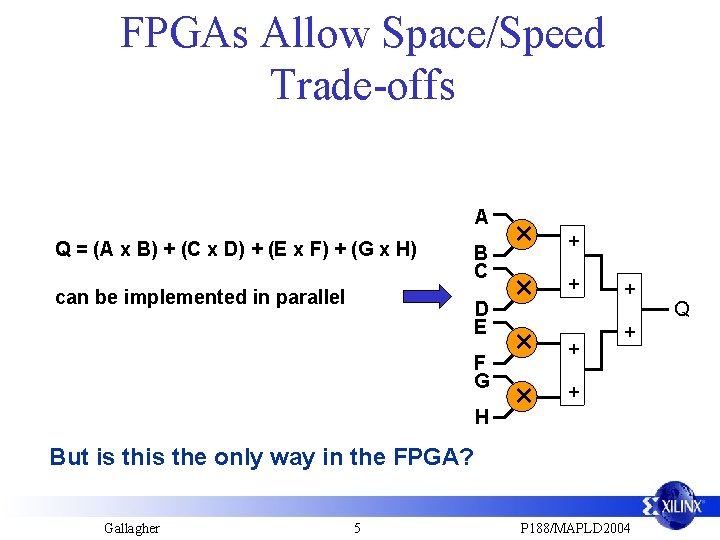
FPGAs Allow Space/Speed Trade-offs A Q = (A x B) + (C x D) + (E x F) + (G x H) can be implemented in parallel B C D E F G H × × + + + But is the only way in the FPGA? Gallagher 5 P 188/MAPLD 2004 Q

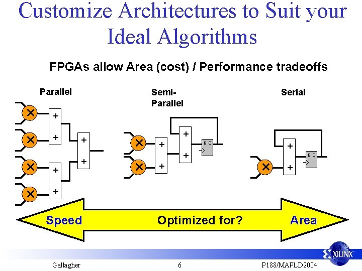
Customize Architectures to Suit your Ideal Algorithms FPGAs allow Area (cost) / Performance tradeoffs Parallel × × Semi. Parallel Serial + + + × × + + DQ + + + × DQ + + Speed Gallagher Optimized for? 6 Area P 188/MAPLD 2004

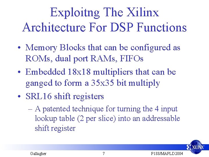
Exploitng The Xilinx Architecture For DSP Functions • Memory Blocks that can be configured as ROMs, dual port RAMs, FIFOs • Embedded 18 x 18 multipliers that can be ganged to form a 35 x 35 bit multiply • SRL 16 shift registers – A patented technique for turning the 4 input lookup table (2 per slice) into an addressable shift register Gallagher 7 P 188/MAPLD 2004

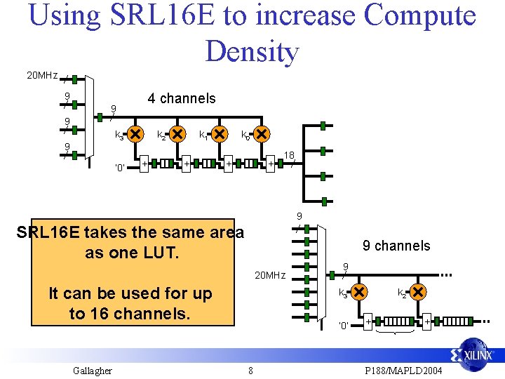
Using SRL 16 E to increase Compute Density 20 MHz 4 channels 9 9 9 k 3 9 ‘ 0’ k 2 + k 1 + k 0 + + 18 9 SRL 16 E takes the same area as one LUT. 9 channels 20 MHz It can be used for up to 16 channels. Gallagher 9 k 3 ‘ 0’ 8 k 2 + + P 188/MAPLD 2004

Xilinx System Generator For DSP – System Generator is a Block Set that resides in Simulink/Matlab environment. – System Generator blocks are bit true and cycle true models of Xilinx’s DSP intellectual property (IP) cores. – Hardware DSP design capture is significantly accelerated due to automatic code generation from Simulink Gallagher 9 P 188/MAPLD 2004

Algorithm Instantiation Considerations • There are cases where following a textbook approach does not necessarily translate into an efficient instantiation • Manipulating the algorithm to exploit features of the architecture can lead to much more efficient instantiations • Modification of a text book algorithm includes how the math is executed as well as over-clocking structures to allow the structures to be time division multiplexed Gallagher 10 P 188/MAPLD 2004

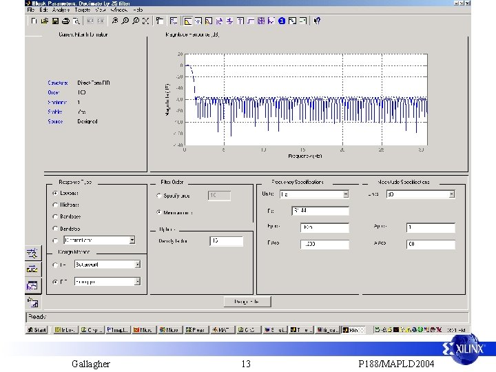
Example 1: Digital Down Conversion • In digital down conversion we need to filter before we decimate to prevent aliasing • These filters can get rather large because the transition band is rather narrow in relation to the sample rate • A text book solution is to step the sample rate down in steps Gallagher 11 P 188/MAPLD 2004

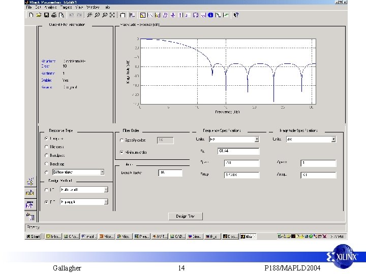
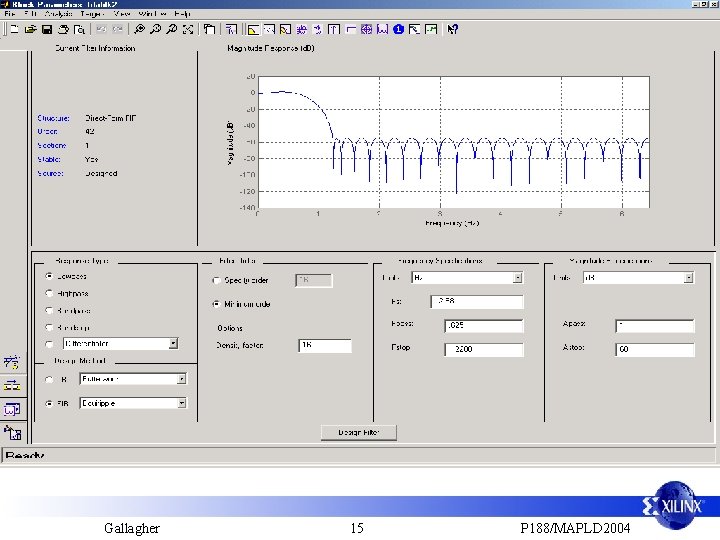
Digital Down Conversion • The following 3 slides show three different filter designs for the down conversion of a. 625 Mhz band of interest that is centered at 20 MHz and sampled at 61. 44 MHz. – The decimation rate is 25 – The final sample rate will be 61. 44/25= 2. 4576 MHz • The next slide shows the filter design needed if decimating by 25 in one step – the total coefficient count is 184 • The two slides after the next show the two filters necessary to decimate in steps, decimating by 5 in each step – The total coefficient count is 11+43=54 Gallagher 12 P 188/MAPLD 2004

Gallagher 13 P 188/MAPLD 2004

Gallagher 14 P 188/MAPLD 2004

Gallagher 15 P 188/MAPLD 2004

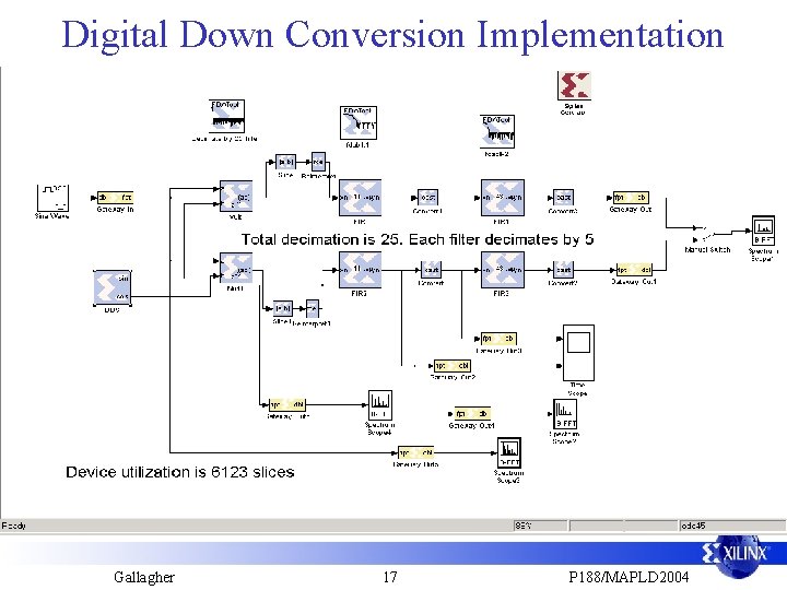
Digital Down Conversion (DDC) Implementation • The following design shows how the DDC function would be implemented using the FIR filter core from the Xilinx Library • The coefficients are automatically loaded into the filter cores • The design has been compiled and was found to use about 6000 logic slices • The fir filter core is a legacy core and is built as an optimized lookup table of coefficients Gallagher 16 P 188/MAPLD 2004

Digital Down Conversion Implementation Gallagher 17 P 188/MAPLD 2004

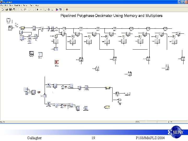
DDC –Another Way • While we were able to exploit the math of DSP to reduce our coefficient count, we did not necessarily exploit the Xilinx architecture. • The next design shows a design that implements the 184 coefficient filter but is significantly smaller in instantiation size then the previous design • This design exploits the memory, embedded multipliers, and SRL 16 s Gallagher 18 P 188/MAPLD 2004

Gallagher 19 P 188/MAPLD 2004

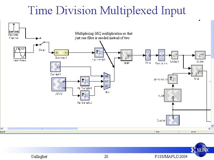
Time Division Multiplexed Input Multiplexing I&Q multiplication so that just one filter is needed instead of two Gallagher 20 P 188/MAPLD 2004

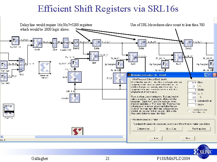
Efficient Shift Registers via SRL 16 s Delay line would require 16 x 50 x 7=5200 registers which would be 2800 logic slices. Gallagher Use of SRL 16 s reduces slice count to less then 700 21 P 188/MAPLD 2004

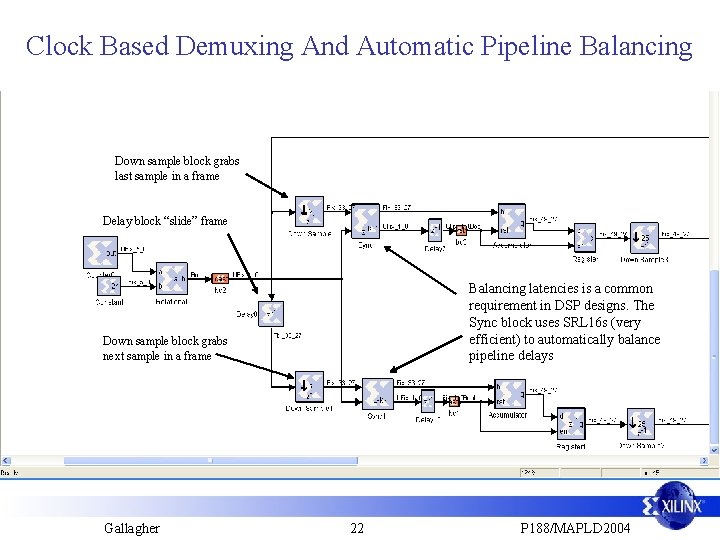
Clock Based Demuxing And Automatic Pipeline Balancing Down sample block grabs last sample in a frame Delay block “slide” frame Balancing latencies is a common requirement in DSP designs. The Sync block uses SRL 16 s (very efficient) to automatically balance pipeline delays Down sample block grabs next sample in a frame Gallagher 22 P 188/MAPLD 2004

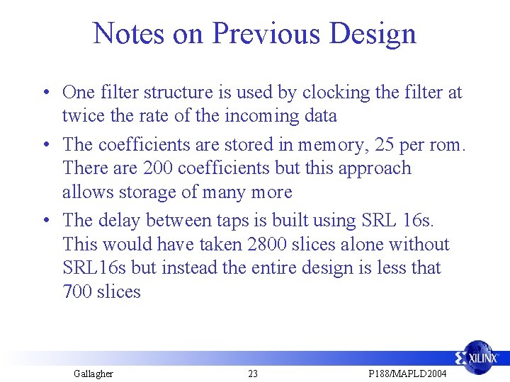
Notes on Previous Design • One filter structure is used by clocking the filter at twice the rate of the incoming data • The coefficients are stored in memory, 25 per rom. There are 200 coefficients but this approach allows storage of many more • The delay between taps is built using SRL 16 s. This would have taken 2800 slices alone without SRL 16 s but instead the entire design is less that 700 slices Gallagher 23 P 188/MAPLD 2004

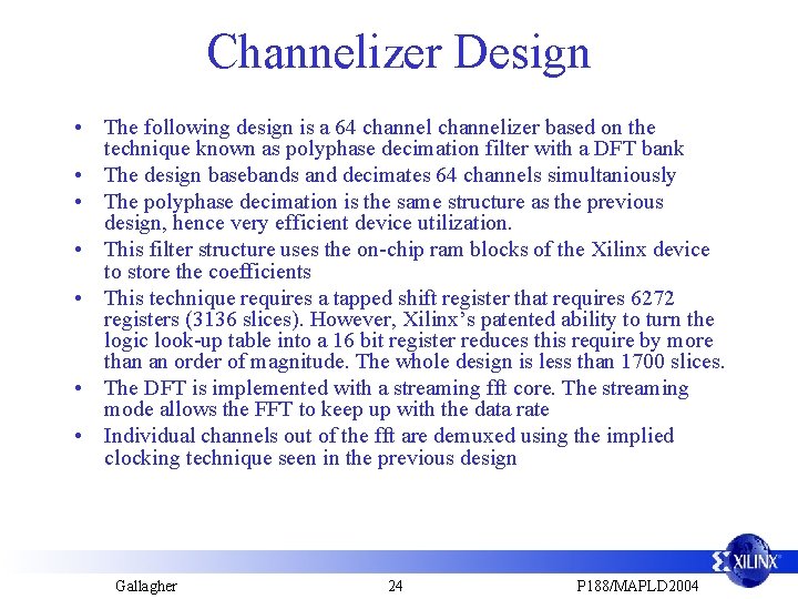
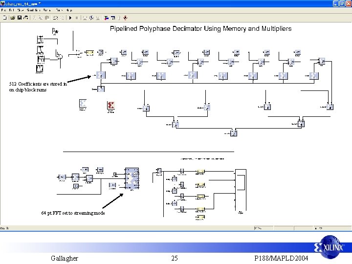
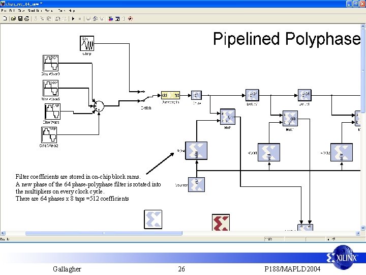
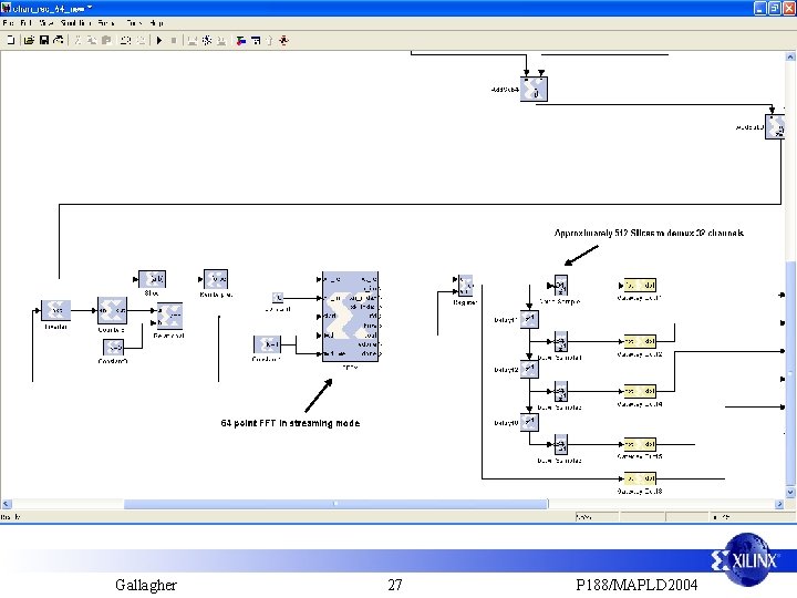
Channelizer Design • The following design is a 64 channelizer based on the technique known as polyphase decimation filter with a DFT bank • The design basebands and decimates 64 channels simultaniously • The polyphase decimation is the same structure as the previous design, hence very efficient device utilization. • This filter structure uses the on-chip ram blocks of the Xilinx device to store the coefficients • This technique requires a tapped shift register that requires 6272 registers (3136 slices). However, Xilinx’s patented ability to turn the logic look-up table into a 16 bit register reduces this require by more than an order of magnitude. The whole design is less than 1700 slices. • The DFT is implemented with a streaming fft core. The streaming mode allows the FFT to keep up with the data rate • Individual channels out of the fft are demuxed using the implied clocking technique seen in the previous design Gallagher 24 P 188/MAPLD 2004

512 Coefficients are stored in on chip block rams 64 pt FFT set to streaming mode Gallagher 25 P 188/MAPLD 2004

Filter coefficients are stored in on-chip block rams. A new phase of the 64 phase-polyphase filter is rotated into the multipliers on every clock cycle. There are 64 phases x 8 taps =512 coefficients Gallagher 26 P 188/MAPLD 2004

Gallagher 27 P 188/MAPLD 2004

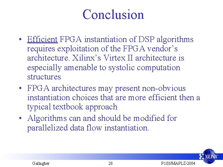
Conclusion • Efficient FPGA instantiation of DSP algorithms requires exploitation of the FPGA vendor’s architecture. Xilinx’s Virtex II architecture is especially amenable to systolic computation structures • FPGA architectures may present non-obvious instantiation choices that are more efficient then a typical textbook approach • Algorithms can and should be modified for parallelized data flow instantiation. Gallagher 28 P 188/MAPLD 2004