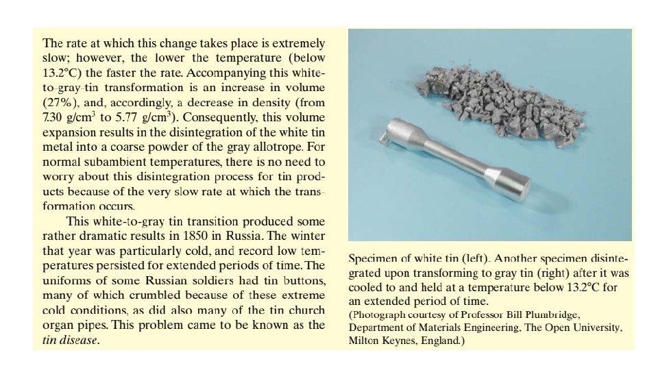
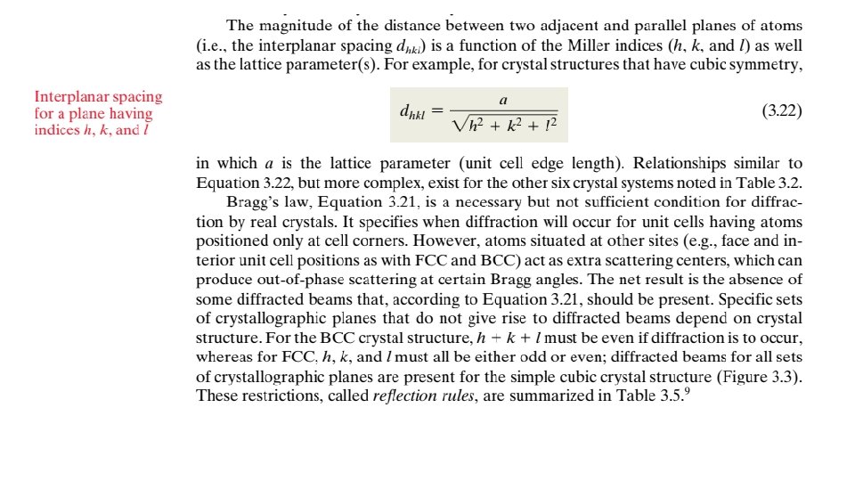
a Xray diffraction photograph for a single crystal
 X-ray diffraction photograph for a single crystal of magnesium. (b) Schematic diagram illustrating")


 a hard-sphere unit cell")
 are thought of as being solid")


 a hard-sphere unit cell")


 is taken as the number of atoms")
,")


 Demonstration of how two waves (labeled 1 and 2) that")


- Slides: 55
(a) X-ray diffraction photograph for a single crystal of magnesium. (b) Schematic diagram illustrating how the spots (i. e. , the diffraction pattern) in (a) are produced. The lead screen blocks out all beams generated from the x-ray source, except for a narrow beam traveling in a single direction. This incident beam is diffracted by individual crystallographic planes in the single crystal (having different orientations), which gives rise to the various diffracted beams that impinge on the photographic plate.
Intersections of these beams with the plate appear as spots when the film is developed. The large spot in the center of (a) is from the incident beam, which is parallel to a [0001] crystallographic direction. It should be noted that the hexagonal symmetry of magnesium’s hexagonal close packed crystal structure [shown in (c)] is indicated by the diffraction spot pattern that was generated. (d) Photograph of a single crystal of magnesium that was cleaved (or split) along a (0001) plane—the flat surface is a (0001) plane. Also, the direction perpendicular to this plane is a [0001] direction.
WHY STUDY The Structure of Crystalline Solids? The properties of some materials are directly related to their crystal structures. For example, pure and undeformed magnesium and beryllium, having one crystal structure, are much more brittle (i. e. , fracture at lower degrees of deformation) than are pure and undeformed metals such as gold and silver that have yet another crystal structure. Furthermore, significant property differences exist between crystalline and noncrystalline materials having the same composition. For example, noncrystalline ceramics and polymers normally are optically transparent; the same materials in crystalline (or semicrystalline) form tend to be opaque or, at best, translucent. 3. 1 INTRODUCTION Chapter 2 was concerned primarily with the various types of atomic bonding, which are determined by the electron structures of the individual atoms. The present discussion is devoted to the next level of the structure of materials, specifically, to some of the arrangements that may be assumed by atoms in the solid state. Within this framework, concepts of crystallinity and noncrystallinity are introduced. For crystalline solids, the notion of crystal structure is presented, specified in terms of a unit cell. The three common crystal structures found in metals are then detailed, along with the scheme by which crystallographic points, directions, and planes are expressed. Single crystals, polycrystalline materials, and noncrystalline materials are considered. Another section of this chapter briefly describes how crystal structures are determined experimentally using x-ray diffraction techniques.
Crystal Structures 3. 2 FUNDAMENTAL CONCEPTS Solid materials may be classified according to the regularity with which atoms or ions are arranged with respect to one another. A crystalline material is one in which the atoms are situated in a repeating or periodic array over large atomic distances—that is, long-range order exists, such that upon solidification, the atoms will position themselves in a relative three-dimensional pattern, in which each atom is bonded to its nearest neighbor atoms. All metals, many ceramic materials, and certain polymers form crystalline structures under normal solidification conditions. For those that do not crystallize, this long-range atomic order is absent; these noncrystalline or amorphous materials are discussed briefly at the end of this chapter. Some of the properties of crystalline solids depend on the crystal structure of the material, the manner in which atoms, ions, or molecules are spatially arranged. There is an extremely large number of different crystal structures all having long-range atomic order; these vary from relatively simple structures for metals to exceedingly complex ones, as displayed by some of the ceramic and polymeric materials. The present discussion deals with several common metallic crystal structures.
Figure 3. 1 For the face-centered cubic crystal structure, (a) a hard-sphere unit cell representation, (b) a reduced sphere unit cell, and (c) an aggregate of many atoms.
When crystalline structures are described, atoms (or ions) are thought of as being solid spheres having well-defined diameters. This is termed the atomic hard-sphere model in which spheres representing nearest-neighbor atoms touch one another. An example of the hard-sphere model for the atomic arrangement found in some of the common elemental metals is displayed in Figure 3. 1 c. In this particular case all the atoms are identical. Sometimes the term lattice is used in the context of crystal structures; in this sense lattice means a three-dimensional array of points coinciding with atom positions (or sphere centers). 3. 3 UNIT CELLS The atomic order in crystalline solids indicates that small groups of atoms form a repetitive pattern. Thus, in describing crystal structures, it is often convenient to subdivide the structure into small repeat entities called unit cells. Unit cells for most crystal structures are parallelepipeds or prisms having three sets of parallel faces; one is drawn within the aggregate of spheres (Figure 3. 1 c), which in this case happens to be a cube. A unit cell is chosen to represent the symmetry of the crystal structure, where all the atom Positions in the crystal may be generated by translations of the unit cell integral distances along each of its edges. Thus, the unit cell is the basic structural unit or building block of the crystal structure and defines the crystal structure by virtue of its geometry and the atom positions within. Convenience usually dictates that parallelepiped corners coincide with centers of the hard-sphere atoms. Furthermore, more than a single unit cell may be chosen for a particular crystal structure; however, we generally use the unit cell having the highest level of geometrical symmetry.
3. 4 METALLIC CRYSTAL STRUCTURES The atomic bonding in this group of materials is metallic and thus nondirectional in nature. Consequently, there are minimal restrictions as to the number and position of nearest-neighbor atoms; this leads to relatively large numbers of nearest neighbors and dense atomic packings for most metallic crystal structures. Also, for metals, when we use the hard-sphere model for the crystal structure, each sphere represents an ion core. Table 3. 1 presents the atomic radii for a number of metals. Three relatively simple crystal structures are found for most of the common metals: face-centered cubic, body centered cubic, and hexagonal close-packed. The Face-Centered Cubic Crystal Structure The crystal structure found for many metals has a unit cell of cubic geometry, with atoms located at each of the corners and the centers of all the cube faces. It is aptly called the face-centered cubic (FCC) crystal structure. Some of the familiar metals having this crystal structure are copper, aluminum, silver, and gold (see also Table 3. 1). Figure 3. 1 a shows a hard-sphere model for the FCC unit cell, whereas in Figure 3. 1 b the atom centers are represented by small circles to provide a better perspective on atom positions. The aggregate of atoms in Figure 3. 1 c represents a section of crystal consisting of many FCC unit cells. These spheres or ion cores touch one another across a face diagonal; the cube edge length a and the atomic radius R are related through
On occasion, we need to determine the number of atoms associated with each unit cell. Depending on an atom’s location, it may be considered to be shared with adjacent unit cells—that is, only some fraction of the atom is assigned to a specific cell. For example, for cubic unit cells, an atom completely within the interior “belongs” to that unit cell, one at a cell face is shared with one other cell, and an atom residing at a corner is shared among eight. The number of atoms per unit cell, N, can be computed using the following formula:
or a total of four whole atoms may be assigned to a given unit cell. This is depicted in Figure 3. 1 a, where only sphere portions are represented within the confines of the cube. The cell is composed of the volume of the cube that is generated from the centers of the corner atoms, as shown in the figure. Corner and face positions are really equivalent—that is, translation of the cube corner from an original corner atom to the center of a face atom will not alter the cell structure.
Two other important characteristics of a crystal structure are the coordination number and the atomic packing factor (APF). For metals, each atom has the same number of nearest-neighbor or touching atoms, which is the coordination number. For face-centered cubic, the coordination number is 12. This may be confirmed by examination of Figure 3. 1 a; the front face atom has four corner nearest-neighbor atoms surrounding it, four face atoms that are in contact from behind, and four other equivalent face atoms residing in the next unit cell to the front (not shown). The APF is the sum of the sphere volumes of all atoms within a unit cell (assuming the atomic hard-sphere model) divided by the unit cell volume— that is, For the FCC structure, the atomic packing factor is 0. 74, which is the maximum packing possible for spheres all having the same diameter. Computation of this APF is also included as an example problem. Metals typically have relatively large atomic packing factors to maximize the shielding provided by the free electron cloud. The Body-Centered Cubic Crystal Structure Another common metallic crystal structure also has a cubic unit cell with atoms located at all eight corners and a single atom at the cube center. This is called a body-centeredcubic (BCC) crystal structure. A collection of spheres depicting this crystal structure is shown in Figure 3. 2 c, whereas Figures 3. 2 a and 3. 2 b are diagrams of BCC unit cells withthe atoms represented by hard-sphere and reducedsphere models, respectively. center and corner atoms touch one another along cube diagonals, and unit cell length a and atomic radius R are related through
Figure 3. 2 For the body-centered cubic crystal structure, (a) a hard-sphere unit cell presentation, (b) a reduced sphere unit cell, and (c) an aggregate of many atoms.
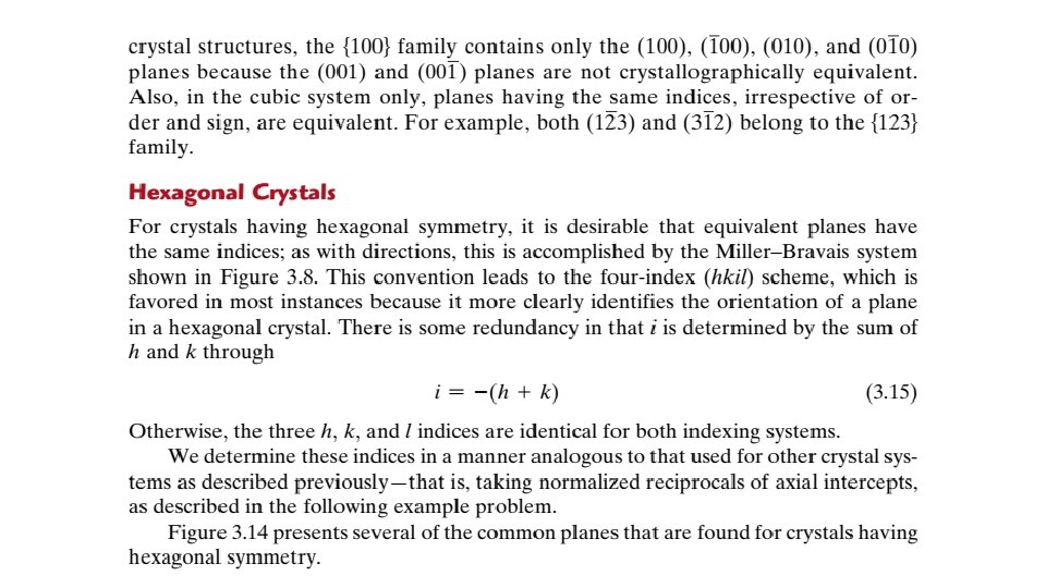
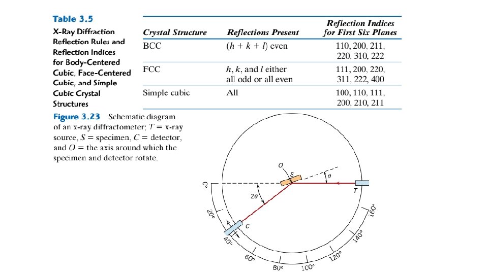
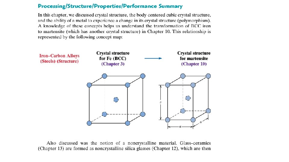
Chromium, iron, tungsten, and several other metals listed in Table 3. 1 exhibit a BCC structure. Each BCC unit cell has eight corner atoms and a single center atom, which is wholly contained within its cell; therefore, from Equation 3. 2, the number of atoms per BCC unit cell is The coordination number for the BCC crystal structure is 8; each center atom has as nearest neighbors its eight corner atoms. Because the coordination number is less for BCC than for FCC, the atomic packing factor is also lower for BCC— 0. 68 versus 0. 74. It is also possible to have a unit cell that consists of atoms situated only at the corners of a cube. This is called the simple cubic (SC) crystal structure; hard-sphere and reduced-sphere models are shown, respectively, in Figures 3. 3 a and 3. 3 b. None of the metallic elements have this crystal structure because of its relatively low atomic packing factor. The only simple-cubic element is polonium, which is considered to be a metalloid (or semi-metal). The Hexagonal Close-Packed Crystal Structure Not all metals have unit cells with cubic symmetry; the final common metallic crystal structure to be discussed has a unit cell that is hexagonal. Figure 3. 4 a shows a reduced sphere unit cell for this structure, which is termed hexagonal close-packed (HCP); an assemblage of several HCP unit cells is presented in Figure 3. 4 b. The top and bottom faces of the unit cell consist of six atoms that form regular
hexagons and surround a single atom in the center. Another plane that provides three additional atoms to the unit cell is situated between the top and bottom planes. The atoms in this midland have as nearest neighbors atoms in both of the adjacent two planes. In order to compute the number of atoms per unit cell for the HCP crystal structure, Equation 3. 2 is modified to read as follows: Figure 3. 3 For the simple cubic crystal structure, (a) a hard-sphere unit cell, and (b) a reduced-sphere unit cell.
That is, one-sixth of each corner atom is assigned to a unit cell (instead of 8 as with the cubic structure). Because for HCP there are 6 corner atoms in each of the top and bottom faces (for a total of 12 corner atoms), 2 face center atoms (one from each of the top and bottom faces), and 3 midplane interior atoms, the value of N for HCP is found, using Equation 3. 5, to be Figure 3. 4 For the hexagonal close-packed crystal structure, (a) a reducedsphere unit cell (a and c represent the short and long edge lengths, respectively), and (b) an aggregate of many atoms.
If a and c represent, respectively, the short and long unit cell dimensions of Figure 3. 4 a, the c/a ratio should be 1. 633; however, for some HCP metals, this ratio deviates from the ideal value. The coordination number and the atomic packing factor for the HCP crystal structure are the same as for FCC: 12 and 0. 74, respectively. The HCP metals include cadmium, magnesium, titanium, and zinc; some of these are listed in Table 3. 1. 3. 5 DENSITY COMPUTATIONS A knowledge of the crystal structure of a metallic solid permits computation of its theoretical density through the relationship 3. 6 POLYMORPHISM AND ALLOTROPY Some metals, as well as nonmetals, may have more than one crystal structure, a phenomenon known as polymorphism.
When found in elemental solids, the condition is often termed allotropy. The prevailing crystal structure depends on both the temperature and the external pressure. One familiar example is found in carbon: graphite is the stable polymorph at ambient conditions, whereas diamond is formed at extremely high pressures. Also, pure iron has a BCC crystal structure at room temperature, which changes to FCC iron at 912 C (1674 F). Most often a modification of the density and other physical properties accompanies a polymorphic transformation.
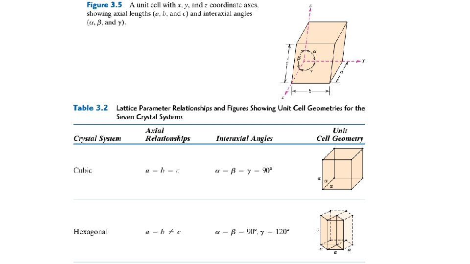
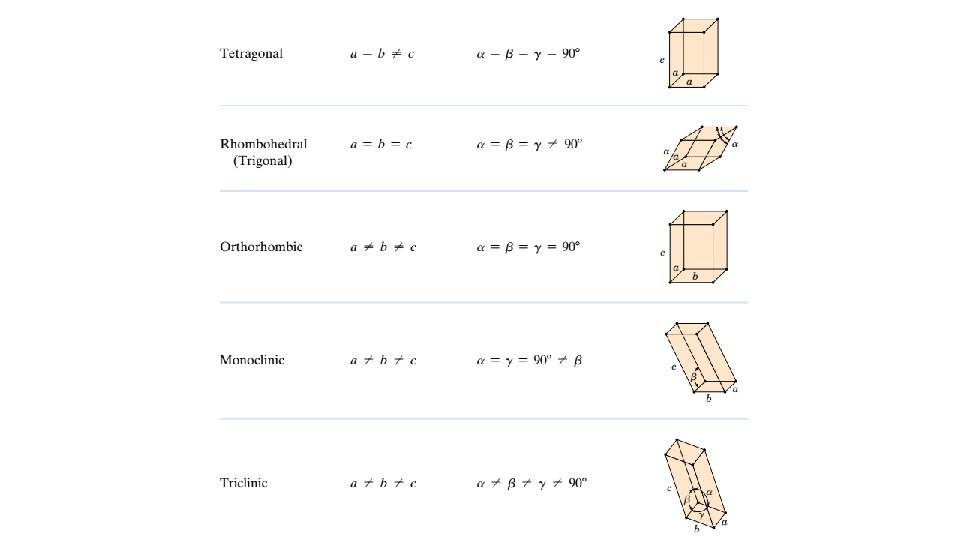
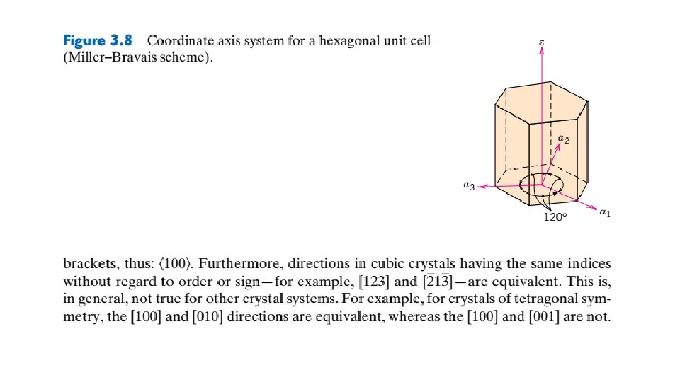
3. 7 CRYSTAL SYSTEMS Because there are many different possible crystal structures, it is sometimes convenient to divide them into groups according to unit cell configurations and/or atomic arrangements. One such scheme is based on the unit cell geometry, that is, the shape of the appropriate unit cell parallelepiped without regard to the atomic positions in the cell. Within this framework, an xyz coordinate system is established with its origin at one of the unit cell corners; each of the x, y, and z axes coincides with one of the three parallelepiped edges that extend from this corner, as illustrated in Figure 3. 5. The unit cell geometry is completely defined in terms of six parameters: the three edge lengths a, b, and c, and the three interaxial angles. These are indicated in Figure 3. 5, and are sometimes termed the lattice parameters of a crystal structure. On this basis there are seven different possible combinations of a, b, and c and , each of which represents a distinct crystal system. These seven crystal systems are cubic, tetragonal, hexagonal, orthorhombic, rhombohedral, monoclinic, and triclinic. The lattice parameter relationships and unit cell sketches for each are represented in Table 3. 2. The cubic system, for which a b c and , has the greatest degree of symmetry. The least symmetry is displayed by the triclinic system, because From the discussion of metallic crystal structures, it should be apparent that both FCC and BCC structures belong to the cubic crystal system, whereas HCP falls within the hexagonal system. The conventional hexagonal unit cell really consists of three parallelepipeds situated as shown in Table 3. 2.
Crystallographic Points, Directions, and Planes When dealing with crystalline materials, it often becomes necessary to specify a particular point within a unit cell, a crystallographic direction, or some crystallographic plane of atoms. Labeling conventions have been established in which three numbers or indices are used to designate point locations, directions, and planes. The basis for determining index values is the unit cell, with a right-handed coordinate system consisting of three (x, y, and z) axes situated at one of the corners and coinciding with the unit cell edges, as shown in Figure 3. 5. For some crystal systems—namely, hexagonal, rhombohedral, monoclinic, and triclinic—the three axes are not mutually perpendicular, as in the familiar Cartesian coordinate scheme. 3. 8 POINT COORDINATES Sometimes it is necessary to specify a lattice position within a unit cell. This is possible using three point coordinate indices: q, r, and s. These indices are fractional multiples of a, b, and c unit cell edge lengths —that is, q is some fractional length of a along the x axis, r is some fractional length of b along the y axis, and similarly for s; or
To illustrate, consider the unit cell in Figure 3. 6, the x-y-z coordinate system with its origin located at a unit cell corner, and the lattice site located at point P. Note how the location of P is related to the products of its q, r, and s coordinate indices and the unit cell edge lengths. 3. 9 CRYSTALLOGRAPHIC DIRECTIONS A crystallographic direction is defined as a line directed between two points, or a vector. The following steps are used to determine three directional indices:
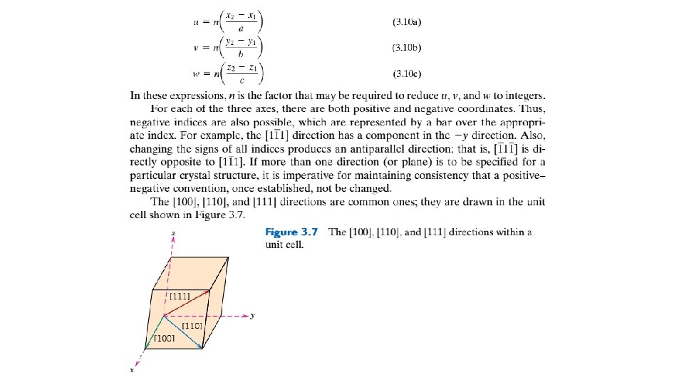
1. A right-handed x-y-z coordinate system is first constructed. As a matter of convenience, its origin may be located at a unit cell corner. 2. The coordinates of two points that lie on the direction vector (referenced to the coordinate system) are determined—for example, for the vector tail, point 1: x 1, y 1, and z 1; whereas for the vector head, point 2: x 2, y 2, and z 2. 3. Tail point coordinates are subtracted from head point components- that is, x 2 - x 1, y 2 - y 1, and z 2 - z 1. 4. These coordinate differences are then normalized in terms of (i. e. , divided by) their respective a, b, and c lattice parameters—that is, which yields a set of three numbers. 5. If necessary, these three numbers are multiplied or divided by a common factor to reduce them to the smallest integer values. 6. The three resulting indices, not separated by commas, are enclosed in square brackets, thus: [u v w]. The u, v, and w integers correspond to the normalized coordinate differences referenced to the x, y, and z axes, respectively. In summary, the u, v, and w indices may be determined using the following equations:
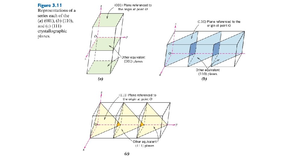
3. 10 CRYSTALLOGRAPHIC PLANES The orientations of planes for a crystal structure are represented in a similar manner. Again, the unit cell is the basis, with the three-axis coordinate system as represented in Figure 3. 5. In all but the hexagonal crystal system, crystallographic planes are specified by three Miller indices as (hkl). Any two planes parallel to each other are equivalent and have identical indices. The procedure used to determine the h, k, and l index numbersis as follows: 1. If the plane passes through the selected origin, either another parallel plane must be constructed within the unit cell by an appropriate translation, or a new origin must be established at the corner of another unit cell. 6 2. At this point, the crystallographic plane either intersects or parallels each of the three axes. The coordinate for the intersection of the crystallographic plane with each of the axes is determined (referenced to the origin of the coordinate system). These intercepts for the x, y, and z axes will be designed by A, B, and C, respectively. 3. The reciprocals of these numbers are taken. A plane that parallels an axis is considered to have an infinite intercept and therefore a zero index. 4. The reciprocals of the intercepts are then normalized in terms of (i. e. , multiplied by) their respective a, b, and c lattice parameters. That is,
5. If necessary, these three numbers are changed to the set of smallest integers by multiplication or by division by a common factor. 6. Finally, the integer indices, not separated by commas, are enclosed within parentheses, thus: (hkl). The h, k, and l integers correspond to the normalized intercept reciprocals referenced to the x, y, and z axes, respectively. In summary, the h, k, and l indices may be determined using the following equations: In these expressions, n is the factor that may be required to reduce h, k, and l to integers. An intercept on the negative side of the origin is indicated by a bar or minus sign positioned over the appropriate index. Furthermore, reversing the directions of all indices specifies another plane parallel to, on the opposite side of, and equidistant from the origin. Several low-index planes are represented in Figure 3. 11. One interesting and unique characteristic of cubic crystals is that planes and directions having the same indices are perpendicular to one another; however, for other crystal systems there are no simple geometrical relationships between planes and directions having the same indices.
3. 11 LINEAR AND PLANAR DENSITIES The two previous sections discussed the equivalency of nonparallel crystallographic directions and planes. Directional equivalency is related to linear density in the sense that, for a particular material, equivalent directions have identical linear densities. The corresponding parameter for crystallographic planes is planar density, and planes having the same planar density values are also equivalent. Linear density (LD) is defined as the number of atoms per unit length whose centers lie on the direction vector for a specific crystallographic direction; that is, The units of linear density are reciprocal length (e. g. , nm 1, m 1). For example, let us determine the linear density of the [110] direction for the FCC crystal structure. An FCC unit cell (reduced sphere) and the [110] direction therein are shown in Figure 3. 15 a. Represented in Figure 3. 15 b are the five atoms that lie on the bottom face of this unit cell; here, the [110] direction vector passes from the center of atom X, through atom Y, and finally to the center of atom Z. With regard to the numbers of atoms, it is necessary to take into account the sharing of atoms with adjacent unit cells (as discussed in Section 3. 4 relative to atomic packing factor computations). Each of the X and Z corner atoms is also shared with one other adjacent unit cell along this [110] direction (i. e. , one-half of each of these atoms belongs to the unit cell being considered), whereas atom Y lies entirely within the unit cell. Thus, there is an equivalence of two atoms along the [110] direction vector in the unit cell. Now, the direction vector length is equal to 4 R (Figure 3. 15 b); thus, from Equation 3. 16, the [110] linear density for FCC is
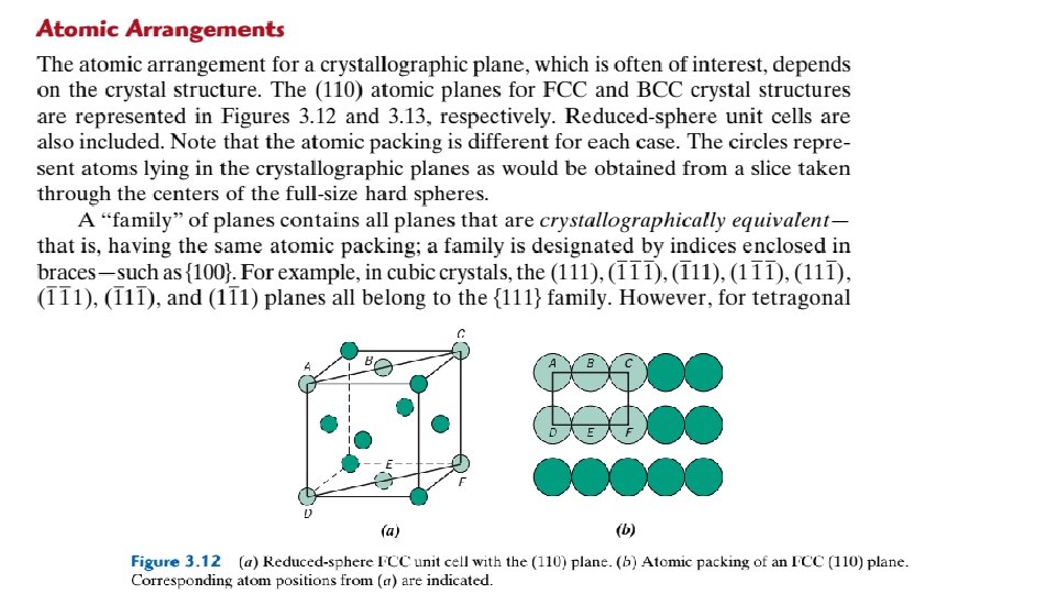
In an analogous manner, planar density (PD) is taken as the number of atoms per unit area that are centered on a particular crystallographic plane, or The units for planar density are reciprocal area (e. g. , nm-2, m-2). For example, consider the section of a (110) plane within an FCC unit cell as represented in Figures 3. 12 a and 3. 12 b.
Although six atoms have centers that lie on this plane (Figure 3. 12 b), only one-quarter of each of atoms A, C, D, and F and one-half of atoms B and E, for a total equivalence of just 2 atoms, are on that plane. Furthermore, the area of this rectangular section is equal to the product of its length and width. From Figure 3. 12 b, the length (horizontal dimension) is equal to 4 R, whereas the width (vertical dimension) is equal to because it corresponds to the FCC unit cell edge length (Equation 3. 1). Thus, the area of this planar region is , and the planar density is determined as follows: Linear and planar densities are important considerations relative to the process of slip— that is, the mechanism by which metals plastically deform (Section 7. 4). Slip occurs on the most densely packed crystallographic planes and, in those planes, along directions having the greatest atomic packing. 3. 12 CLOSE-PACKED CRYSTAL STRUCTURES You may remember from the discussion on metallic crystal structures (Section 3. 4) that both facecentered cubic and hexagonal close-packed crystal structures have atomic packing factors of 0. 74, which is the most efficient packing of equal-size spheres or atoms. In addition to unit cell representations, these two crystal structures may be described in terms of close-packed planes of atoms (i. e. , planes having a maximum atom or sphere-packing density); a portion of one such plane is illustrated in Figure 3. 16 a. Both crystal structures may be generated by the stacking of these close-packed planes on top of one another; the difference between the two structures lies in the stacking sequence.
Let the centers of all the atoms in one close-packed plane be labeled A. Associated with this plane are two sets of equivalent triangular depressions formed by three adjacent atoms, into which the next closepacked plane of atoms may rest. Those having the triangle vertex pointing up are arbitrarily designated as B positions, whereas the remaining depressions are those with the down vertices, which are marked C in Figure 3. 16 a. A second close-packed plane may be positioned with the centers of its atoms over either B or C sites; at this point, both are equivalent. Suppose that the B positions are arbitrarily chosen; the stacking sequence is termed AB, which is illustrated in Figure 3. 16 b. The real distinction between FCC and HCP lies in where third close-packed layer is positioned. For HCP, the centers of this layer are aligned directly above the original. A positions. This stacking sequence, ABABAB. . . , is repeated over and over. Of course, the ACACAC. . . arrangement would be equivalent. These close-packed planes for HCP are (0001)-type planes, and the correspondence between this and the unit cell representation is shown in Figure 3. 17.
For the face-centered crystal structure, the centers of the third plane are situated over the C sites of the first plane (Figure 3. 18 a). This yields an ABCABCABC. . . stacking sequence; that is, the atomic alignment repeats every third plane. It is more difficult to correlate the stacking of close-packed planes to the FCC unit cell. However, this relationship is demonstrated in Figure 3. 18 b. These planes are of the (111) type; an FCC unit cell is outlined on the upper left-hand front face of Figure 3. 18 b to provide perspective. The significance of these FCC and HCP close-packed planes.
specify crystallographic planes and directions in terms of directional and Miller indices; furthermore, on occasion it is important to ascertain the atomic and ionic arrangements of particular crystallographic planes. Also, the crystal structures of a number of ceramic materials may be generated by the stacking of close-packed planes of ions
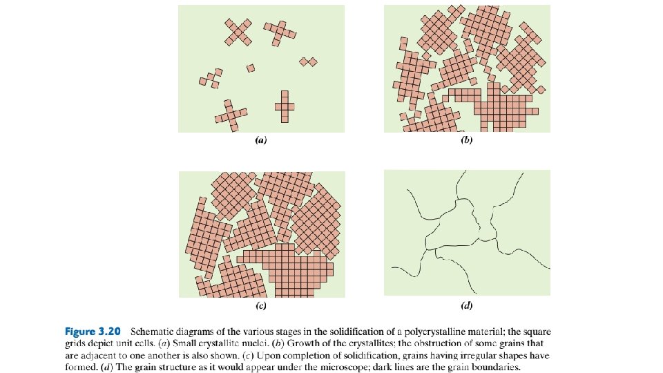
Crystalline and Noncrystalline Materials 3. 13 SINGLE CRYSTALS For a crystalline solid, when the periodic and repeated arrangement of atoms is perfector extends throughout the entirety of the specimen without interruption, the result is a single crystal. All unit cells interlock in the same way and have the same orientation. Single crystals exist in nature, but they can also be produced artificially. They are ordinarily difficult to grow because the environment must be carefully controlled. If the extremities of a single crystal are permitted to grow without any external constraint, the crystal assumes a regular geometric shape having flat faces, as with some of the gemstones; the shape is indicative of the crystal structure. A garnet single crystal is shown in Figure 3. 19. Within the past few years, single crystals have become extremely important in many modern technologies, in particular electronic microcircuits, which employ single crystals of silicon and other semiconductors. 3. 14 POLYCRYSTALLINE MATERIALS Most crystalline solids are composed of a collection of many small crystals or grains; such materials are termed polycrystalline. Various stages in the solidification of a polycrystalline specimen are represented schematically in Figure 3. 20. Initially, small crystals or nuclei form at various positions.
These have random crystallographic orientations, as indicated by the square grids. The small grains grow by the successive addition from the surrounding liquid of atoms to the structure of each. The extremities of adjacent grains impinge on one another as the solidification process approaches completion. As indicated in Figure 3. 20, the crystallographic orientation varies from grain to grain. Also, there exists some atomic mismatch within the region where two grains meet; this area, called a grain boundary.
3. 15 ANISOTROPY The physical properties of single crystals of some substances depend on the crystallographic direction in which measurements are taken. For example, the elastic modulus, the electrical conductivity, and the index of refraction may have different values in the [100] and [111] directions. This directionality of properties is termed anisotropy, and it is associated with the variance of atomic or ionic spacing with crystallographic direction. Substances in which measured properties are independent of the direction of measurement are isotropic. The extent and magnitude of anisotropic effects in crystalline materials are functions of the symmetry of the crystal structure; the degree of anisotropy increases with decreasing structural symmetry—triclinic structures normally are highly anisotropic. The modulus of elasticity values at [100], [110], and [111] orientations for several metals are presented in Table 3. 4.
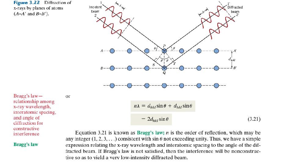
3. 16 X-RAY DIFFRACTION: DETERMINATION OF CRYSTAL STRUCTURES Historically, much of our understanding regarding the atomic and molecular arrangements in solids has resulted from x-ray diffraction investigations; furthermore, x-rays are still very important in developing new materials. We now give a brief overview of the diffraction phenomenon and how, using x-rays, atomic interplanar distances and crystal structures are deduced. The Diffraction Phenomenon Diffraction occurs when a wave encounters a series of regularly spaced obstacles that (1) are capable of scattering the wave, and (2) have spacings that are comparable in magnitude to the wavelength. Furthermore, diffraction is a consequence of specific phase relationships established between two or more waves that have been scattered by the obstacles. Consider waves 1 and 2 in Figure 3. 21 a, which have the same wavelength and are in phase at point O–O-. Now let us suppose that both waves are scattered
Figure 3. 21 (a) Demonstration of how two waves (labeled 1 and 2) that have the same wavelength l and remain in phase after a scattering event (waves 1 - and 2 -) constructively interfere with one another. The amplitudes of the scattered waves add together in the resultant wave. (b) Demonstration of how two waves (labeled 3 and 4) that have the same wavelength and become out of phase after a scattering event (waves 3 and 4 -) destructively interfere with one another. The amplitudes of the two scattered waves cancel one another.
X-Ray Diffraction and Bragg’s Law
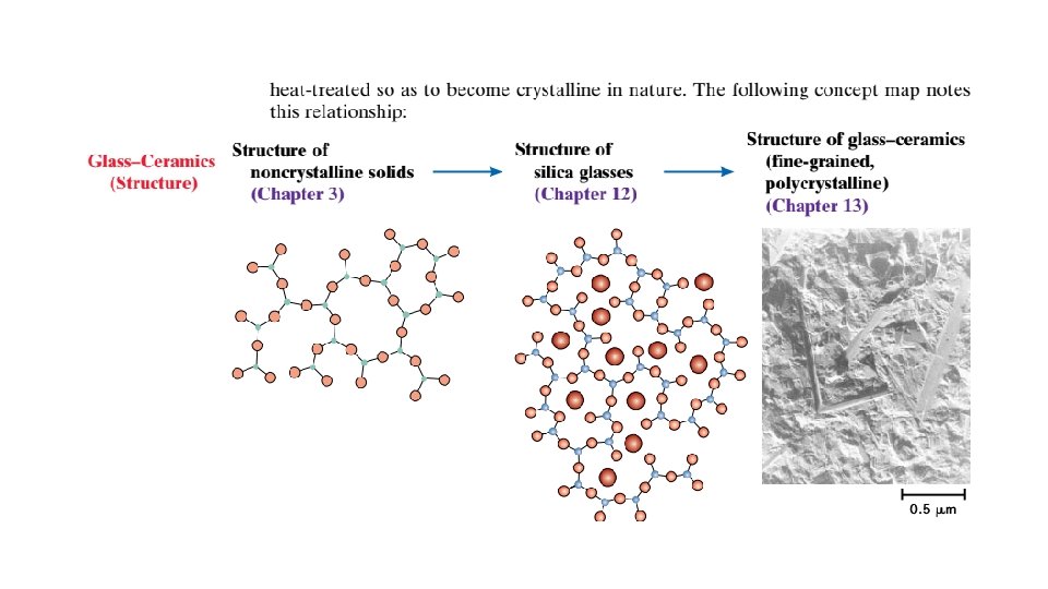
Furthermore, rapidly cooling through the freezing temperature favors the formation of a noncrystalline solid, because little time is allowed for the ordering process. Metals normally form crystalline solids, but some ceramic materials are crystalline, whereas others—the inorganic glasses—are amorphous. Polymers may be completely noncrystalline or semicrystalline consisting of varying degrees of crystallinity.