
A wide dynamic range Charge Sensitive Amplifier June


- Slides: 12
A wide dynamic range Charge Sensitive Amplifier June 5, 2013 PV/BG Luigi Gaioni
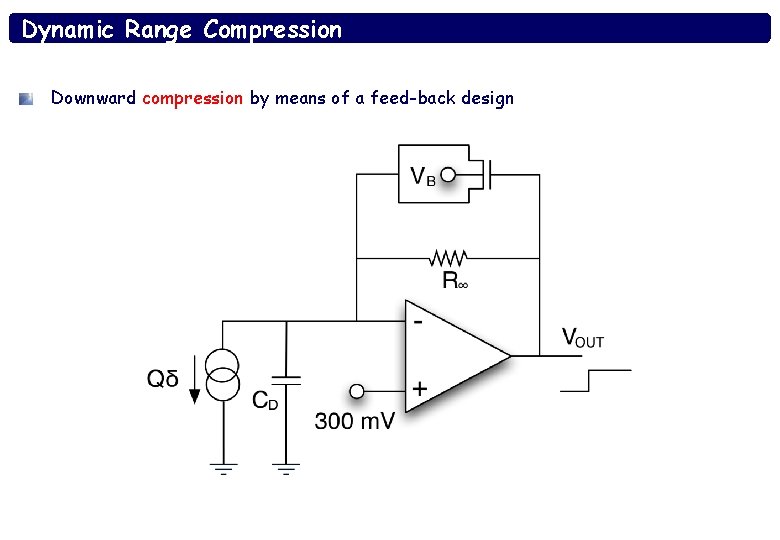
Dynamic Range Compression Downward compression by means of a feed-back design
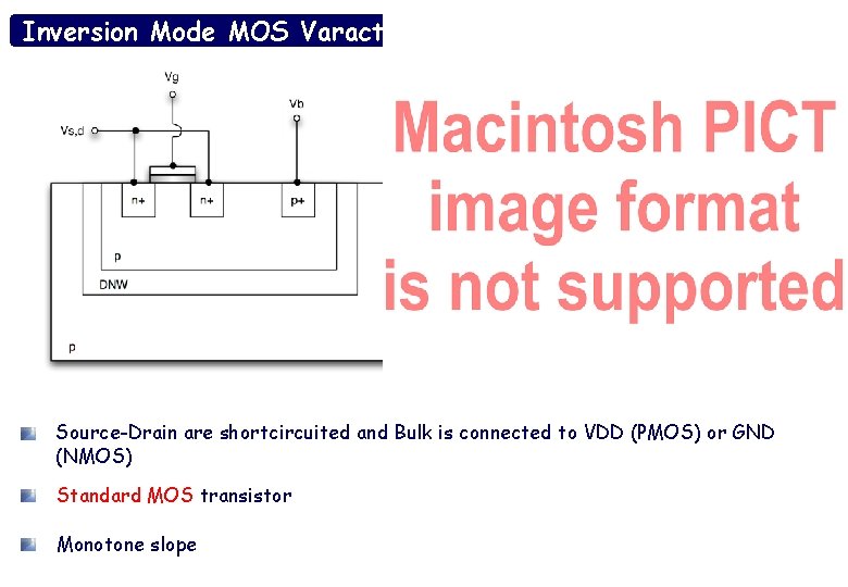
Inversion Mode MOS Varactor Source-Drain are shortcircuited and Bulk is connected to VDD (PMOS) or GND (NMOS) Standard MOS transistor Monotone slope
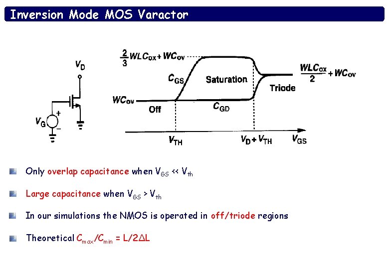
Inversion Mode MOS Varactor Only overlap capacitance when VGS << Vth Large capacitance when VGS > Vth In our simulations the NMOS is operated in off/triode regions Theoretical Cmax/Cmin = L/2∆L
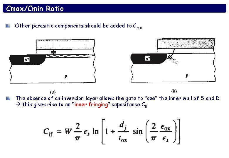
Cmax/Cmin Ratio Other parasitic components should be added to Cmin The absence of an inversion layer allows the gate to “see” the inner wall of S and D this gives rise to an “inner fringing” capacitance Cif
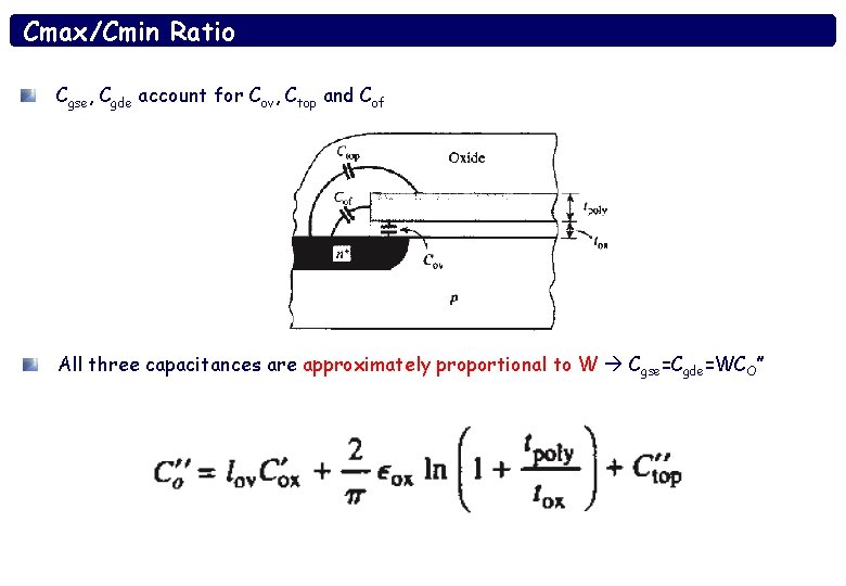
Cmax/Cmin Ratio Cgse, Cgde account for Cov, Ctop and Cof All three capacitances are approximately proportional to W Cgse=Cgde=WCO’’
CSA signal amplitude VS energy High-Energy Gain Low-Energy Gain (LEG) increases by increasing Vsb (increasing Vth) High-Energy Gain (HEG) depends on the WL product Equivalent Feedback capacitance Ceq = (d. Vout/d. Qin)-1
MOS geometry effects on LEG increases with decreasing W (1/W behavior) 1/L behavior for L > 10 µm Why LEG is affected by L and Vth ?
MOS geometry effects on LEG We get Cmin for VGS < 0 For VGS ≈ 0 Ceq depends on Vth and on gate dimension MOSFET has to be DC biased with negative VGS
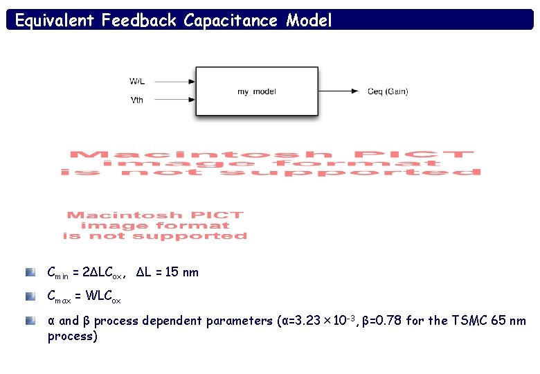
Equivalent Feedback Capacitance Model Cmin = 2ΔLCox, ΔL = 15 nm Cmax = WLCox α and β process dependent parameters (α=3. 23× 10 -3, β=0. 78 for the TSMC 65 nm process)
Model validation
Model validation