A Simplified MIPS Processor in Verilog Data Memory
![Instruction Memory • The most straightforward way of loading a program: ram[0] ram[1] ram[2] Instruction Memory • The most straightforward way of loading a program: ram[0] ram[1] ram[2]](https://slidetodoc.com/presentation_image/09d090ea01392862aa3b1bfecb489b80/image-7.jpg)
![ALU module MIPSALU (ALUctl, A, B, ALUOut, Zero); input [3: 0] ALUctl; input [31: ALU module MIPSALU (ALUctl, A, B, ALUOut, Zero); input [3: 0] ALUctl; input [31:](https://slidetodoc.com/presentation_image/09d090ea01392862aa3b1bfecb489b80/image-11.jpg)
![Sign Extension module Sign. Extend (in, out); input [15: 0] in; output [31: 0] Sign Extension module Sign. Extend (in, out); input [15: 0] in; output [31: 0]](https://slidetodoc.com/presentation_image/09d090ea01392862aa3b1bfecb489b80/image-12.jpg)
![Supporting a new instruction else if (instr[31: 26] == 6'b 000001) //lwr begin Reg. Supporting a new instruction else if (instr[31: 26] == 6'b 000001) //lwr begin Reg.](https://slidetodoc.com/presentation_image/09d090ea01392862aa3b1bfecb489b80/image-20.jpg)
- Slides: 20

A Simplified MIPS Processor in Verilog

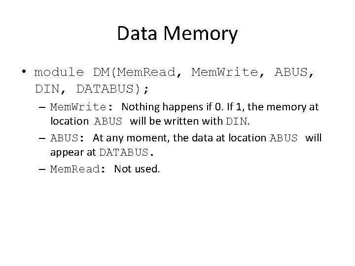
Data Memory • module DM(Mem. Read, Mem. Write, ABUS, DIN, DATABUS); – Mem. Write: Nothing happens if 0. If 1, the memory at location ABUS will be written with DIN. – ABUS: At any moment, the data at location ABUS will appear at DATABUS. – Mem. Read: Not used.

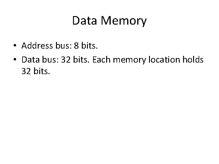
Data Memory • Address bus: 8 bits. • Data bus: 32 bits. Each memory location holds 32 bits.

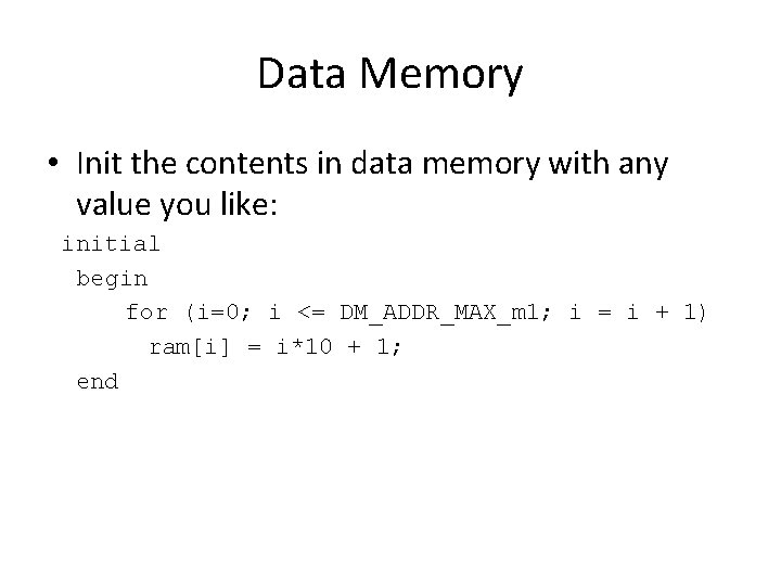
Data Memory • Init the contents in data memory with any value you like: initial begin for (i=0; i <= DM_ADDR_MAX_m 1; i = i + 1) ram[i] = i*10 + 1; end

Instruction Memory • module IM(CSB, WRB, ABUS, DATABUS); – CSB: chip select. If 0, selected. If 1, not selected. – WRB: Not used. – ABUS: Address bus. At any moment, if chip is selected, the data at location ABUS will appear at DATABUS.

Instruction Memory • Address bus: 8 bits. • Data bus: 32 bits. Each memory location holds 32 bits.
![Instruction Memory The most straightforward way of loading a program ram0 ram1 ram2 Instruction Memory • The most straightforward way of loading a program: ram[0] ram[1] ram[2]](https://slidetodoc.com/presentation_image/09d090ea01392862aa3b1bfecb489b80/image-7.jpg)
Instruction Memory • The most straightforward way of loading a program: ram[0] ram[1] ram[2] ram[3] ram[4] ram[5] ram[6] ram[7] ram[8] ram[9] = = = = = 32'b 001000000000000000; 32'b 00100000001000000001; 32'b 001000010000000010; 32'b 00100000011000000011; 32'b 00000000000000000000000000000000; 32'b 00000000000000000000000000000000; // // // addi nop nop nop $0, $1, $2, $3, 0 1 2 3

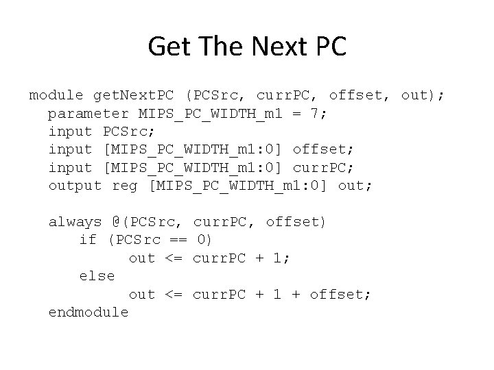
Get The Next PC module get. Next. PC (PCSrc, curr. PC, offset, out); parameter MIPS_PC_WIDTH_m 1 = 7; input PCSrc; input [MIPS_PC_WIDTH_m 1: 0] offset; input [MIPS_PC_WIDTH_m 1: 0] curr. PC; output reg [MIPS_PC_WIDTH_m 1: 0] out; always @(PCSrc, curr. PC, offset) if (PCSrc == 0) out <= curr. PC + 1; else out <= curr. PC + 1 + offset; endmodule

PC • module MIPSPC(clk, new. PC, PC); • Just an 8 -bit D-flip-flop.

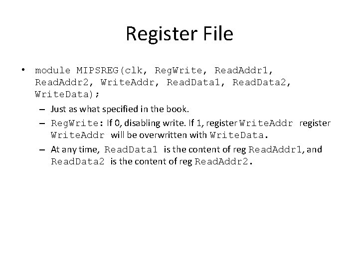
Register File • module MIPSREG(clk, Reg. Write, Read. Addr 1, Read. Addr 2, Write. Addr, Read. Data 1, Read. Data 2, Write. Data); – Just as what specified in the book. – Reg. Write: If 0, disabling write. If 1, register Write. Addr will be overwritten with Write. Data. – At any time, Read. Data 1 is the content of reg Read. Addr 1, and Read. Data 2 is the content of reg Read. Addr 2.
![ALU module MIPSALU ALUctl A B ALUOut Zero input 3 0 ALUctl input 31 ALU module MIPSALU (ALUctl, A, B, ALUOut, Zero); input [3: 0] ALUctl; input [31:](https://slidetodoc.com/presentation_image/09d090ea01392862aa3b1bfecb489b80/image-11.jpg)
ALU module MIPSALU (ALUctl, A, B, ALUOut, Zero); input [3: 0] ALUctl; input [31: 0] A, B; output reg [31: 0] ALUOut; output Zero; assign Zero = (ALUOut==0); //Zero is true if ALUOut is 0; goes anywhere always @(ALUctl, A, B) //reevaluate if these change case (ALUctl) 0: ALUOut <= A & B; 1: ALUOut <= A | B; 2: ALUOut <= A + B; 6: ALUOut <= A - B; 7: ALUOut <= A < B ? 1: 0; 12: ALUOut <= ~(A | B); // result is nor default: ALUOut <= 0; //default to 0, should not happen; endcase endmodule
![Sign Extension module Sign Extend in out input 15 0 in output 31 0 Sign Extension module Sign. Extend (in, out); input [15: 0] in; output [31: 0]](https://slidetodoc.com/presentation_image/09d090ea01392862aa3b1bfecb489b80/image-12.jpg)
Sign Extension module Sign. Extend (in, out); input [15: 0] in; output [31: 0] out; assign out[15: 0] = in[15: 0]; assign out[31: 16] = in[15]; endmodule

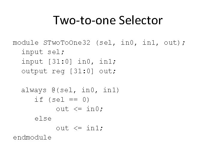
Two-to-one Selector module STwo. To. One 32 (sel, in 0, in 1, out); input sel; input [31: 0] in 0, in 1; output reg [31: 0] out; always @(sel, in 0, in 1) if (sel == 0) out <= in 0; else out <= in 1; endmodule

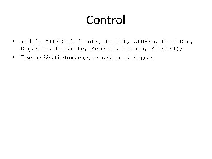
Control • module MIPSCtrl (instr, Reg. Dst, ALUSrc, Mem. To. Reg, Reg. Write, Mem. Read, branch, ALUCtrl); • Take the 32 -bit instruction, generate the control signals.

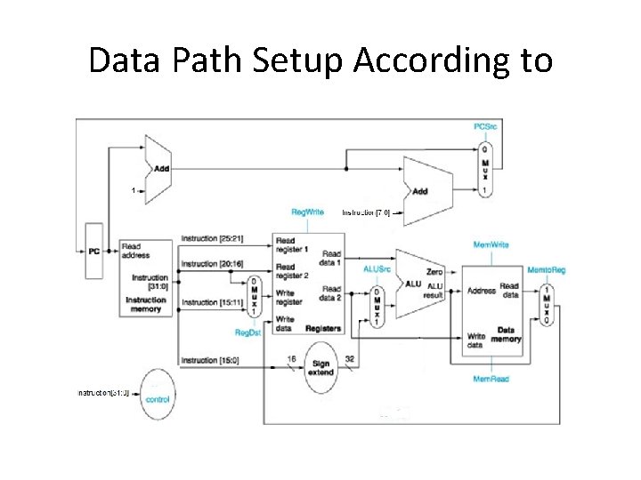
Data Path Setup According to

Supported instructions • add, sub, addi, lw, sw, beq.

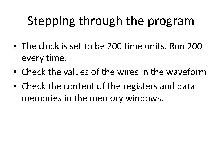
Stepping through the program • The clock is set to be 200 time units. Run 200 every time. • Check the values of the wires in the waveform • Check the content of the registers and data memories in the memory windows.

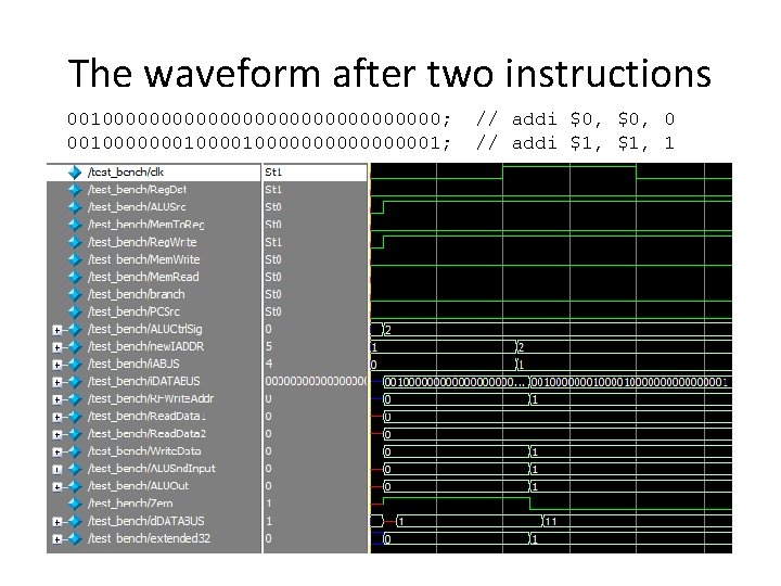
The waveform after two instructions 001000000000000000; 00100000001000000001; // addi $0, 0 // addi $1, 1

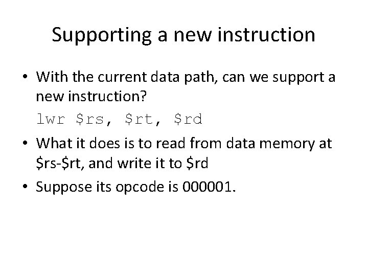
Supporting a new instruction • With the current data path, can we support a new instruction? lwr $rs, $rt, $rd • What it does is to read from data memory at $rs-$rt, and write it to $rd • Suppose its opcode is 000001.
![Supporting a new instruction else if instr31 26 6b 000001 lwr begin Reg Supporting a new instruction else if (instr[31: 26] == 6'b 000001) //lwr begin Reg.](https://slidetodoc.com/presentation_image/09d090ea01392862aa3b1bfecb489b80/image-20.jpg)
Supporting a new instruction else if (instr[31: 26] == 6'b 000001) //lwr begin Reg. Dst <= 1; ALUSrc <= 0; Mem. To. Reg <= 1; Reg. Write <= 1; Mem. Read <= 1; Mem. Write <= 0; branch <= 0; ALUCtrl <= 4'b 0110; end