A RADHARD LVDS CHIP TRANSISTOR LEVEL DESIGN ASPECTS







- Slides: 26

A RADHARD LVDS CHIP: TRANSISTOR LEVEL DESIGN ASPECTS JAN WOUTERS AMICSA 2018, LEUVEN PUBLIC

OUTLINE § Introduction & context § Design aspects § § § transmitter common mode receiver extended common mode SET hardening SET hardness & “HOT” PMOS cold spare ESD § § § receiver failsafe receiver oscillation current reference decoupling (on-chip, damped) power down receiver testability § Future work 2 AMICSA 2018

INTRODUCTION & CONTEXT 3

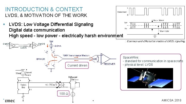
INTRODUCTION & CONTEXT LVDS, & MOTIVATION OF THE WORK § LVDS: Low Voltage Differential Signaling Digital data communication High speed - low power - electrically harsh environment CMOS LVDS Space. Wire: - standard for communication in spacecrafts - physical level: LVDS Current driven 100 4 AMICSA 2018

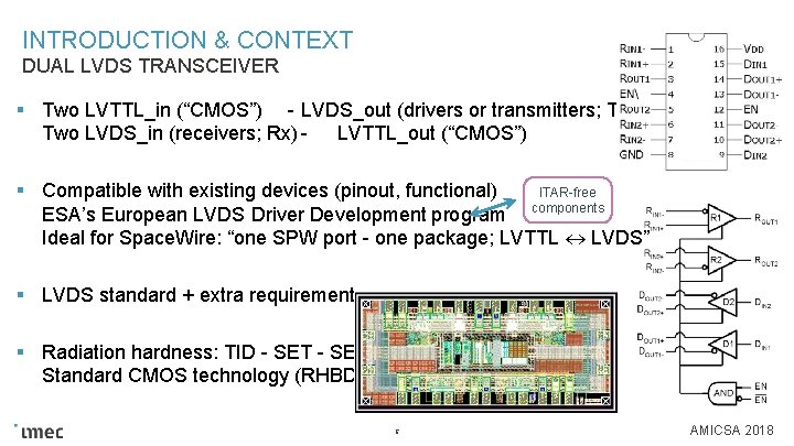
INTRODUCTION & CONTEXT DUAL LVDS TRANSCEIVER § Two LVTTL_in (“CMOS”) - LVDS_out (drivers or transmitters; Tx) Two LVDS_in (receivers; Rx) - LVTTL_out (“CMOS”) § Compatible with existing devices (pinout, functional) ITAR-free ESA’s European LVDS Driver Development program components Ideal for Space. Wire: “one SPW port - one package; LVTTL LVDS” § LVDS standard + extra requirements § Radiation hardness: TID - SET - SEL Standard CMOS technology (RHBD) 5 AMICSA 2018

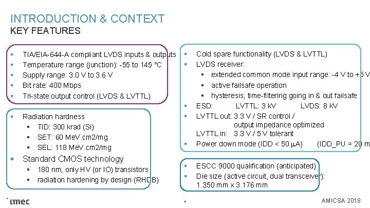
INTRODUCTION & CONTEXT KEY FEATURES § § § § TIA/EIA-644 -A compliant LVDS inputs & outputs Temperature range (junction): -55 to 145 °C Supply range: 3. 0 V to 3. 6 V Bit rate: 400 Mbps Tri-state output control (LVDS & LVTTL) Radiation hardness § TID: 300 krad (Si) § SET: 60 Me. V. cm 2/mg § SEL: 118 Me. V. cm 2/mg Standard CMOS technology § 180 nm; only HV (or IO) transistors § radiation hardening by design (RHDB) § § § § 6 Cold spare functionality (LVDS & LVTTL) LVDS receiver: § extended common mode input range: -4 V to +5 V § active failsafe operation § hysteresis; time-filtering going in & out failsafe ESD: LVTTL: 3 k. V LVDS: 8 k. V LVTTL out: 3. 3 V / SR control / output impedance optimized LVTTL in: 3. 3 V / 5 V tolerant Power down mode (IDD < 50 A) (IDD_PU = 20 m ESCC 9000 qualification (anticipated) Die size (active circuit, dual transceiver): 1. 350 mm x 3. 176 mm AMICSA 2018

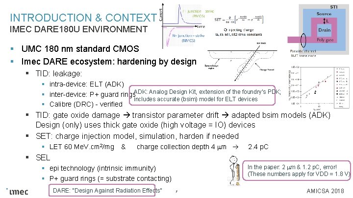
INTRODUCTION & CONTEXT IMEC DARE 180 U ENVIRONMENT § UMC 180 nm standard CMOS § Imec DARE ecosystem: hardening by design § TID: leakage: § intra-device: ELT (ADK) § inter-device: P+ guard rings. ADK: Analog Design Kit, extension of the foundry’s PDK; includes accurate (bsim) model for ELT devices § Calibre (DRC) - verified § TID: gate oxide damage transistor parameter drift adapted bsim models (ADK) Design (only) uses thick gate oxide (high voltage = IO) devices § SET: charge injection model, simulation, harden if needed § LET 60 Me. V. cm 2/mg & charge collection depth 4 m 2. 4 p. C § SEL In the paper: 2 m & 1. 2 p. C, error! (These numbers apply for VDD = 1. 8 V) § epi technology (intrinsic immunity) § P+ guard rings (= substrate contacting) DARE: “Design Against Radiation Effects” 7 AMICSA 2018

DESIGN ASPECTS 8

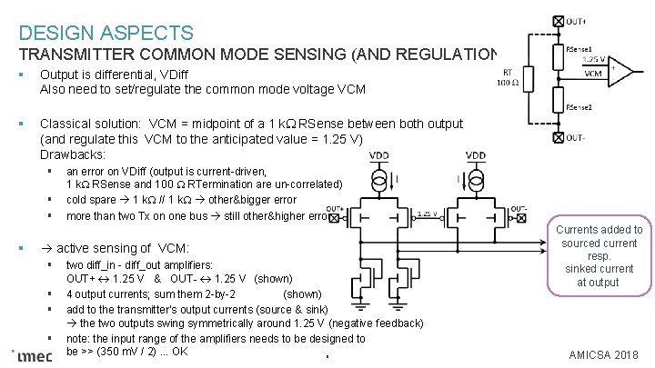
DESIGN ASPECTS TRANSMITTER COMMON MODE SENSING (AND REGULATION) § Output is differential, VDiff Also need to set/regulate the common mode voltage VCM § Classical solution: VCM = midpoint of a 1 k RSense between both output (and regulate this VCM to the anticipated value = 1. 25 V) Drawbacks: § § an error on VDiff (output is current-driven, 1 k RSense and 100 RTermination are un-correlated) cold spare 1 k // 1 k other&bigger error more than two Tx on one bus still other&higher error active sensing of VCM: § § two diff_in - diff_out amplifiers: OUT+ 1. 25 V & OUT - 1. 25 V (shown) 4 output currents; sum them 2 -by-2 (shown) add to the transmitter’s output currents (source & sink) the two outputs swing symmetrically around 1. 25 V (negative feedback) note: the input range of the amplifiers needs to be designed to be >> (350 m. V / 2). . . OK 9 Currents added to sourced current resp. sinked current at output AMICSA 2018

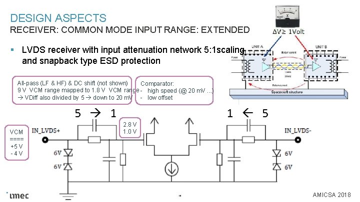
DESIGN ASPECTS RECEIVER: COMMON MODE INPUT RANGE: EXTENDED § LVDS receiver with input attenuation network 5: 1 scaling and snapback type ESD protection All-pass (LF & HF) & DC shift (not shown) Comparator: 9 V VCM range mapped to 1. 8 V VCM range - high speed (@ 20 m. V. . . ) VDiff also divided by 5 down to 20 m. V - low offset VCM ==== +5 V -4 V 2. 8 V 1. 0 V 10 AMICSA 2018

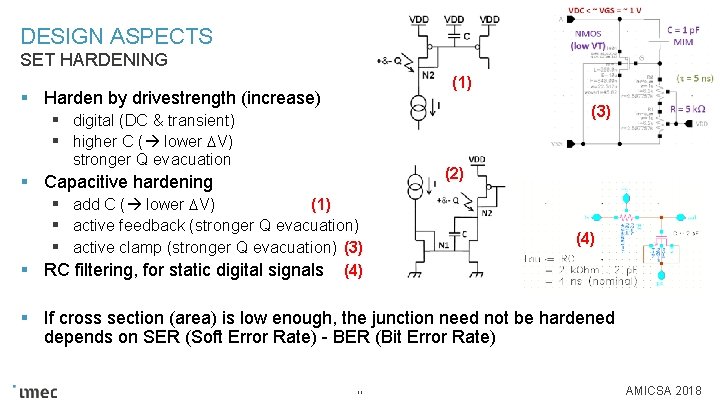
DESIGN ASPECTS SET HARDENING (1) § Harden by drivestrength (increase) (3) § digital (DC & transient) § higher C ( lower V) stronger Q evacuation (2) § Capacitive hardening § add C ( lower V) (1) § active feedback (stronger Q evacuation) (2) § active clamp (stronger Q evacuation) (3) § RC filtering, for static digital signals (4) § If cross section (area) is low enough, the junction need not be hardened depends on SER (Soft Error Rate) - BER (Bit Error Rate) 11 AMICSA 2018

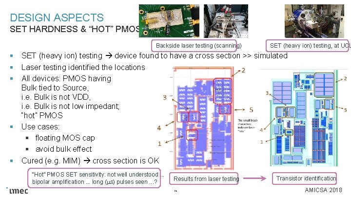
DESIGN ASPECTS SET HARDNESS & “HOT” PMOS Backside laser testing (scanning) § § § SET (heavy ion) testing, at UCL SET (heavy ion) testing device found to have a cross section >> simulated Laser testing identified the locations All devices: PMOS having Bulk tied to Source, i. e. Bulk is not VDD, i. e. Bulk is not low impedant; “hot” PMOS Use cases: § floating MOS cap § avoid bulk effect Cured (e. g. MIM) cross section is OK “Hot” PMOS SET sensitivity: not well understood. . . bipolar amplification. . . long ( s) pulses seen. . . ? Results from laser testing 12 Transistor identification AMICSA 2018

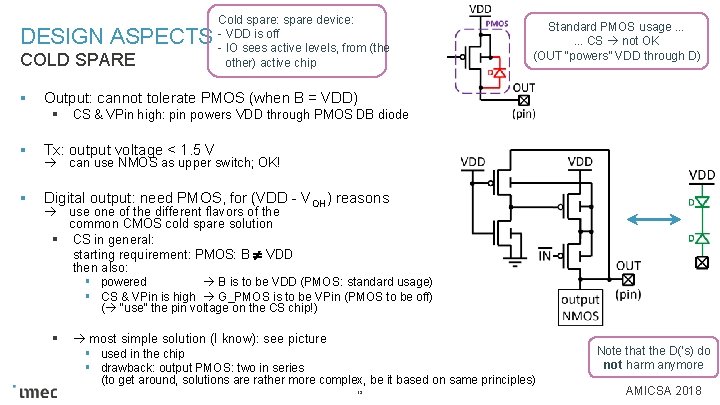
DESIGN ASPECTS COLD SPARE § Cold spare: spare device: - VDD is off - IO sees active levels, from (the other) active chip Standard PMOS usage. . . CS not OK (OUT “powers” VDD through D) Output: cannot tolerate PMOS (when B = VDD) § CS & VPin high: pin powers VDD through PMOS DB diode § Tx: output voltage < 1. 5 V § Digital output: need PMOS, for (VDD - VOH) reasons can use NMOS as upper switch; OK! use one of the different flavors of the common CMOS cold spare solution § CS in general: starting requirement: PMOS: B VDD then also: § powered B is to be VDD (PMOS: standard usage) § CS & VPin is high G_PMOS is to be VPin (PMOS to be off) ( “use” the pin voltage on the CS chip!) § most simple solution (I know): see picture § used in the chip § drawback: output PMOS: two in series Note that the D(’s) do not harm anymore (to get around, solutions are rather more complex, be it based on same principles) 13 AMICSA 2018

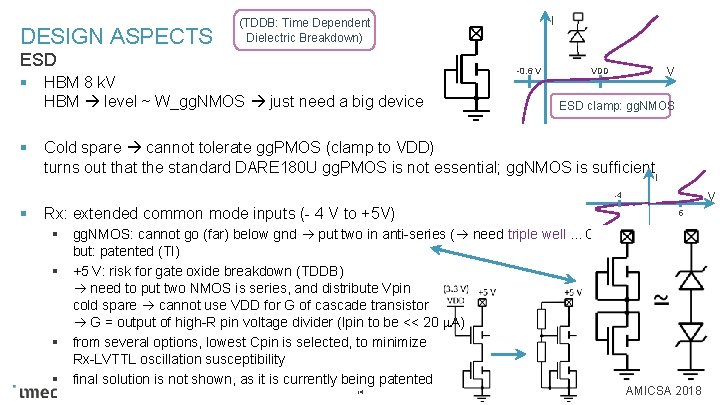
DESIGN ASPECTS ESD § § I (TDDB: Time Dependent Dielectric Breakdown) HBM 8 k. V HBM level ~ W_gg. NMOS just need a big device -0. 6 V V VDD ESD clamp: gg. NMOS Cold spare cannot tolerate gg. PMOS (clamp to VDD) turns out that the standard DARE 180 U gg. PMOS is not essential; gg. NMOS is sufficient I V -4 § Rx: extended common mode inputs (- 4 V to +5 V) § gg. NMOS: cannot go (far) below gnd put two in anti-series ( need triple well. . . OK) but: patented (TI) § +5 V: risk for gate oxide breakdown (TDDB) need to put two NMOS is series, and distribute Vpin cold spare cannot use VDD for G of cascade transistor G = output of high-R pin voltage divider (Ipin to be << 20 A) § from several options, lowest Cpin is selected, to minimize Rx-LVTTL oscillation susceptibility § final solution is not shown, as it is currently being patented 14 5 AMICSA 2018

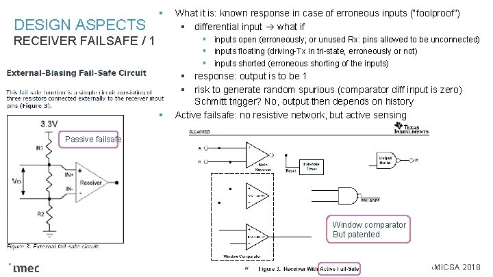
DESIGN ASPECTS § RECEIVER FAILSAFE / 1 What it is: known response in case of erroneous inputs (“foolproof”) § differential input what if § inputs open (erroneously; or unused Rx: pins allowed to be unconnected) § inputs floating (driving-Tx in tri-state, erroneously or not) § inputs shorted (erroneous shorting of the inputs) § § response: output is to be 1 § risk to generate random spurious (comparator diff input is zero) Schmitt trigger? No, output then depends on history Active failsafe: no resistive network, but active sensing Passive failsafe Window comparator But patented 15 AMICSA 2018

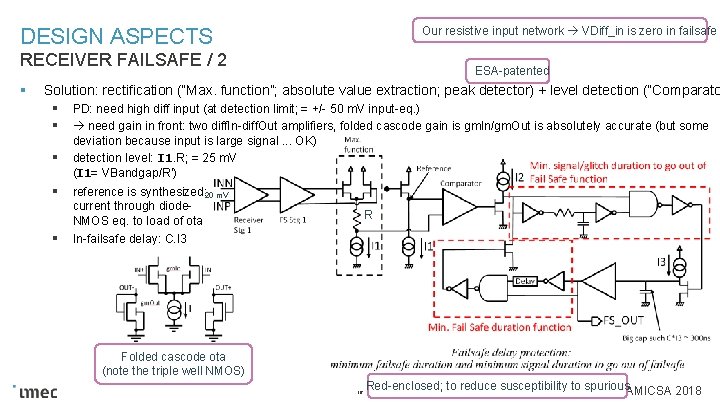
Our resistive input network VDiff_in is zero in failsafe DESIGN ASPECTS RECEIVER FAILSAFE / 2 § ESA-patented Solution: rectification (“Max. function”; absolute value extraction; peak detector) + level detection (“Comparato § § § PD: need high diff input (at detection limit; = +/- 50 m. V input-eq. ) need gain in front: two diff. In-diff. Out amplifiers, folded cascode gain is gm. In/gm. Out is absolutely accurate (but some deviation because input is large signal. . . OK) detection level: I 1. R; = 25 m. V (I 1= VBandgap/R’) reference is synthesized: 20 m. V current through diode. NMOS eq. to load of ota In-failsafe delay: C. I 3 R Folded cascode ota (note the triple well NMOS) 16 Red-enclosed; to reduce susceptibility to spurious. AMICSA 2018

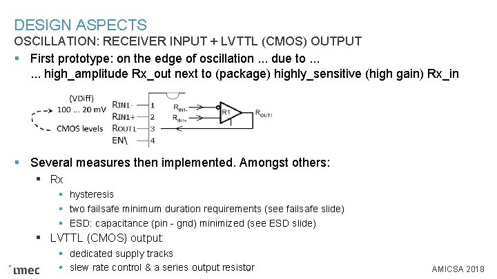
DESIGN ASPECTS OSCILLATION: RECEIVER INPUT + LVTTL (CMOS) OUTPUT § First prototype: on the edge of oscillation. . . due to. . . high_amplitude Rx_out next to (package) highly_sensitive (high gain) Rx_in § Several measures then implemented. Amongst others: § Rx § hysteresis § two failsafe minimum duration requirements (see failsafe slide) § ESD: capacitance (pin - gnd) minimized (see ESD slide) § LVTTL (CMOS) output: § dedicated supply tracks § slew rate control & a series output resistor 17 AMICSA 2018

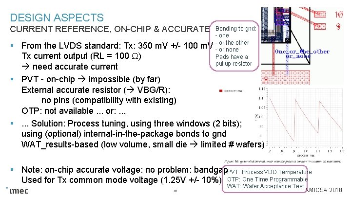
DESIGN ASPECTS CURRENT REFERENCE, ON-CHIP & ACCURATE Bonding to gnd: - one - or the other - or none Pads have a pullup resistor § From the LVDS standard: Tx: 350 m. V +/- 100 m. V Tx current output (RL = 100 ) need accurate current § PVT - on-chip impossible (by far) External accurate resistor ( VBG/R): no pins (compatibility with existing) OTP: not available. . . or: . . . §. . . Solution: Process tuning, using three windows (2 bits); using (optional) internal-in-the-package bonds to gnd WAT_results-based (low volume, small die limited # wafers) § Note: on-chip accurate voltage: no problem: bandgap. PVT: Process VDD Temperature Used for Tx common mode voltage (1. 25 V +/- 10%) OTP: One Time Programmable 18 WAT: Wafer Acceptance Test AMICSA 2018

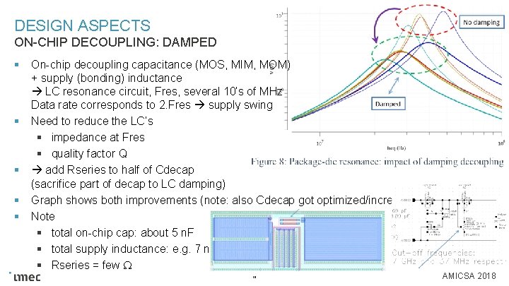
DESIGN ASPECTS ON-CHIP DECOUPLING: DAMPED § § § On-chip decoupling capacitance (MOS, MIM, MOM) + supply (bonding) inductance LC resonance circuit, Fres, several 10’s of MHz Data rate corresponds to 2. Fres supply swing Need to reduce the LC’s § impedance at Fres § quality factor Q add Rseries to half of Cdecap (sacrifice part of decap to LC damping) Graph shows both improvements (note: also Cdecap got optimized/increased) Note § total on-chip cap: about 5 n. F § total supply inductance: e. g. 7 n. H § Rseries = few 19 AMICSA 2018

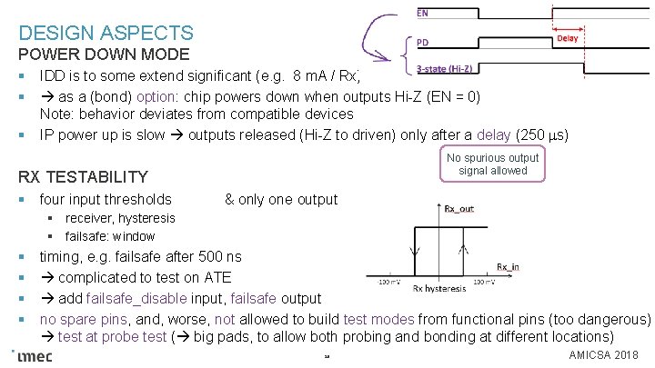
DESIGN ASPECTS POWER DOWN MODE § § § IDD is to some extend significant (e. g. 8 m. A / Rx) as a (bond) option: chip powers down when outputs Hi-Z (EN = 0) Note: behavior deviates from compatible devices IP power up is slow outputs released (Hi-Z to driven) only after a delay (250 s) No spurious output signal allowed RX TESTABILITY § four input thresholds & only one output § receiver, hysteresis § failsafe: window § § timing, e. g. failsafe after 500 ns complicated to test on ATE add failsafe_disable input, failsafe output no spare pins, and, worse, not allowed to build test modes from functional pins (too dangerous) test at probe test ( big pads, to allow both probing and bonding at different locations) 20 AMICSA 2018

FUTURE WORK 21

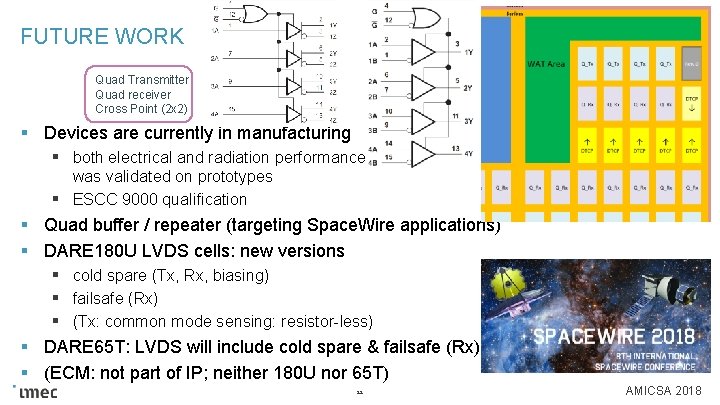
FUTURE WORK Quad Transmitter Quad receiver Cross Point (2 x 2) § Devices are currently in manufacturing § both electrical and radiation performance was validated on prototypes § ESCC 9000 qualification § Quad buffer / repeater (targeting Space. Wire applications) § DARE 180 U LVDS cells: new versions § cold spare (Tx, Rx, biasing) § failsafe (Rx) § (Tx: common mode sensing: resistor-less) § DARE 65 T: LVDS will include cold spare & failsafe (Rx) § (ECM: not part of IP; neither 180 U nor 65 T) 22 AMICSA 2018

ACKNOWLEDGEMENT / CO-AUTHORS: L. BERTI, S. ZAGROCKI, G. THYS, S. REDANT IMEC V. VASSILEV NOVORELL J. ILSTAD, R. JANSEN ESA

NEXT ACTIVITY TODAY AT 17: 00. . . 24 AMICSA 2018

25 AMICSA 2018

PUBLIC