
A Presentation on Unit 1 Diode Circuits By
A Presentation on Unit 1. Diode Circuits By, ASST. PROF. P. D. JADHAV DYPIEMR, AK
Content • • • P-N Junction diode Half wave rectifier Full wave rectifier Bridge wave rectifier Rectifier circuits with C filter Clipper & Clamper circuits Voltage multiplier circuits Zener diode Light emitting diode Photodiode
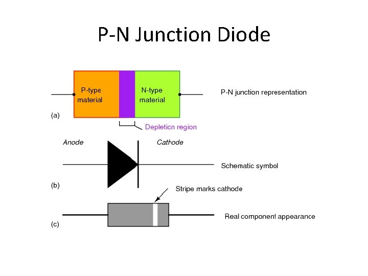
P-N Junction Diode
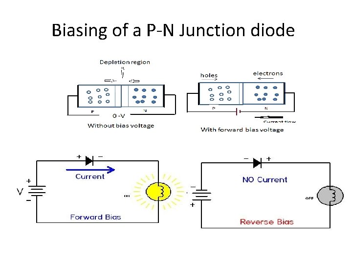
Biasing of a P-N Junction diode
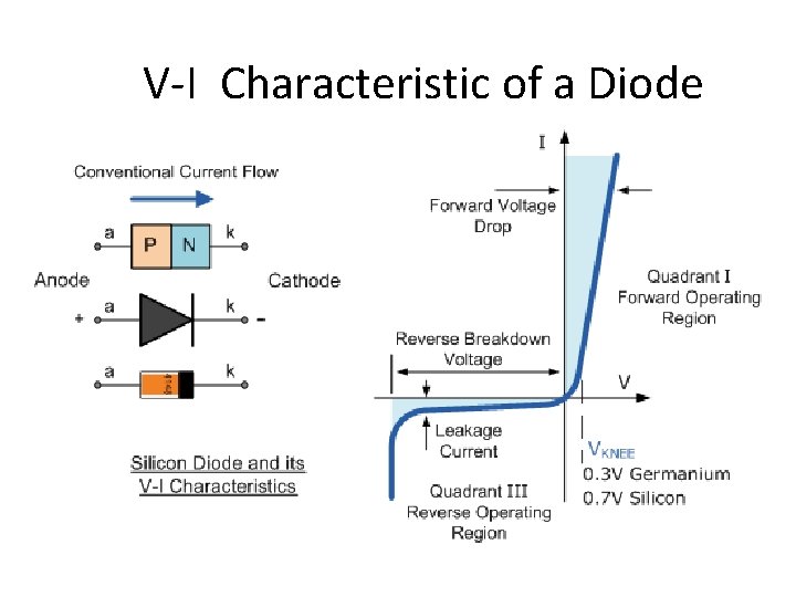
V-I Characteristic of a Diode
Rectifier * Rectifiers convert ac power to dc power. • Rectifiers form the basis for electronic power suppliers and battery charging circuits. • Types of Rectifier – 1) Half Wave Rectifier 2) Full Wave Rectifier 3) Bridge Wave Rectifier
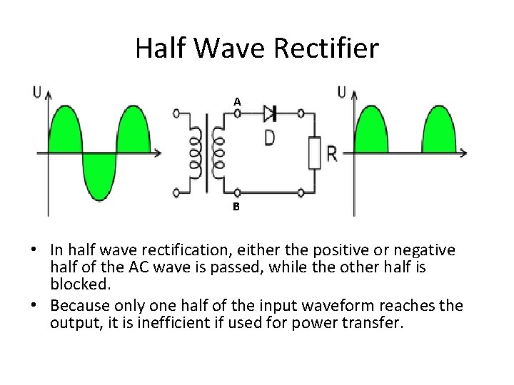
Half Wave Rectifier A B • In half wave rectification, either the positive or negative half of the AC wave is passed, while the other half is blocked. • Because only one half of the input waveform reaches the output, it is inefficient if used for power transfer.
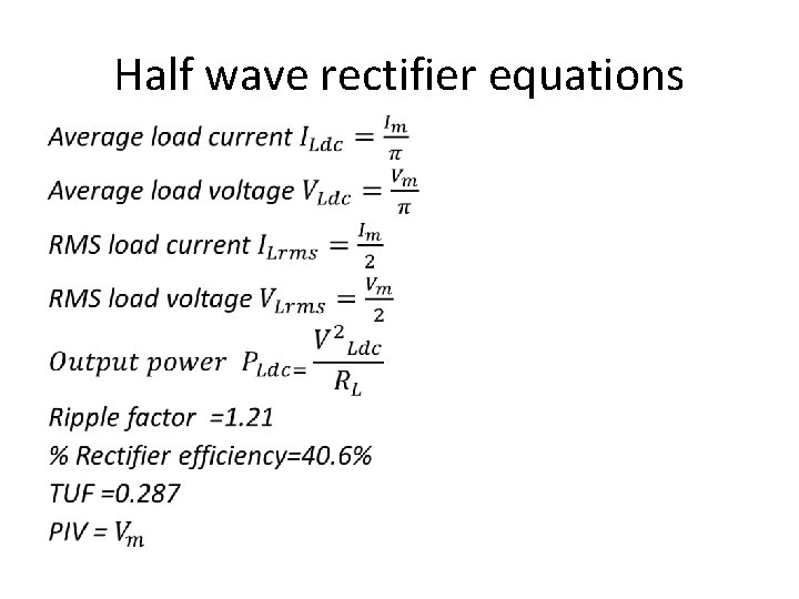
Half wave rectifier equations •
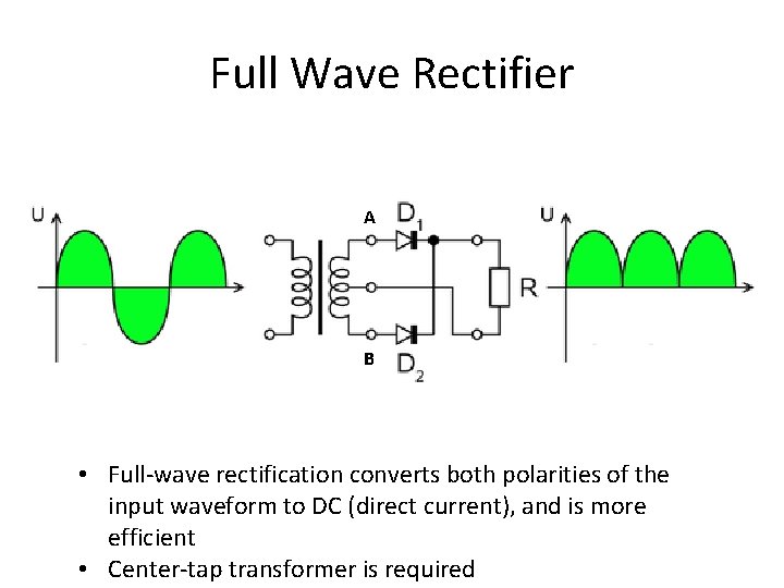
Full Wave Rectifier A B • Full-wave rectification converts both polarities of the input waveform to DC (direct current), and is more efficient • Center-tap transformer is required
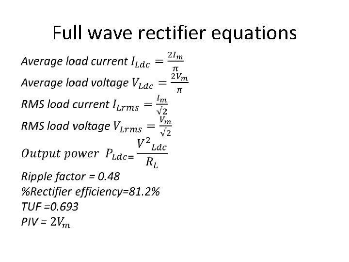
Full wave rectifier equations •
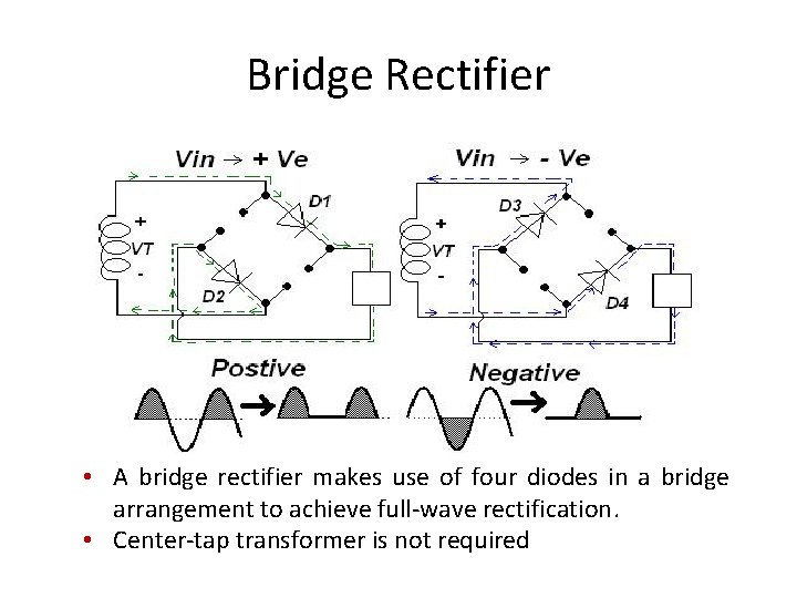
Bridge Rectifier • A bridge rectifier makes use of four diodes in a bridge arrangement to achieve full-wave rectification. • Center-tap transformer is not required
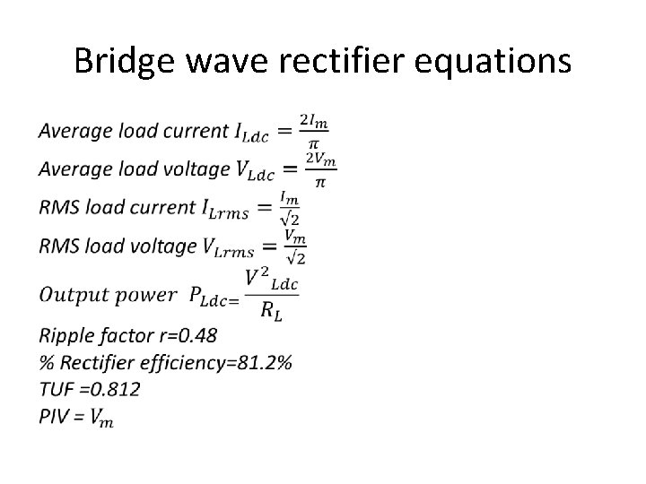
Bridge wave rectifier equations •
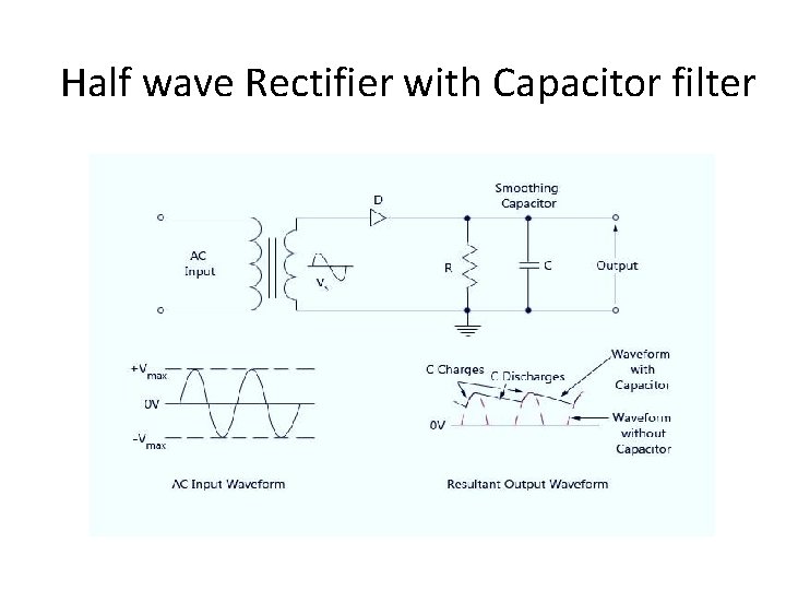
Half wave Rectifier with Capacitor filter
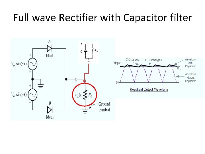
Full wave Rectifier with Capacitor filter
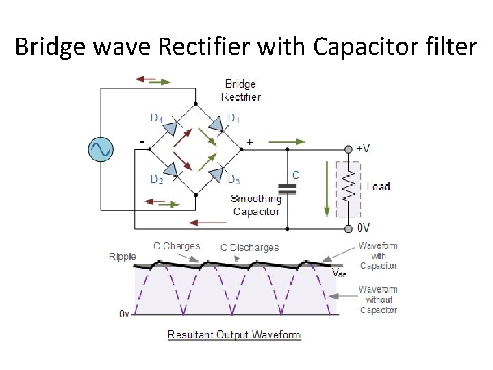
Bridge wave Rectifier with Capacitor filter
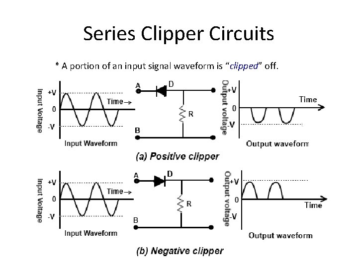
Series Clipper Circuits * A portion of an input signal waveform is “clipped” off.
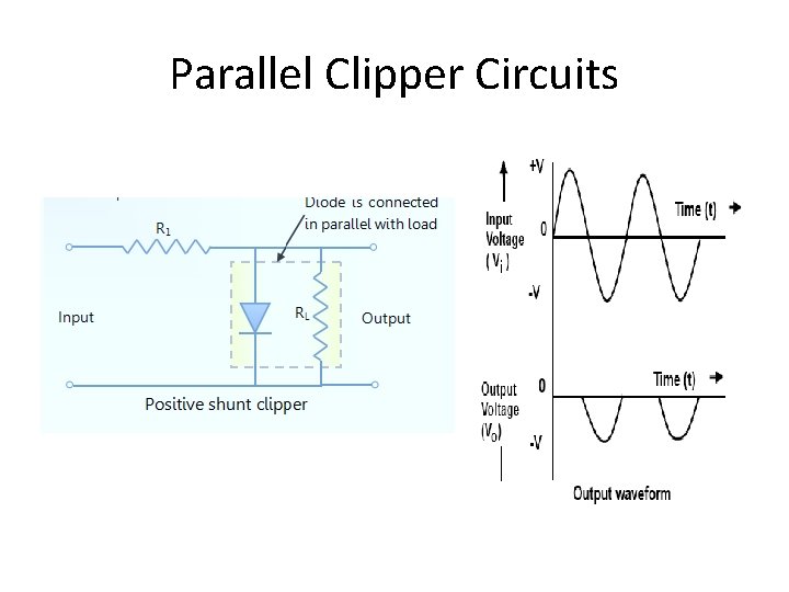
Parallel Clipper Circuits

Biased Clipper Circuit
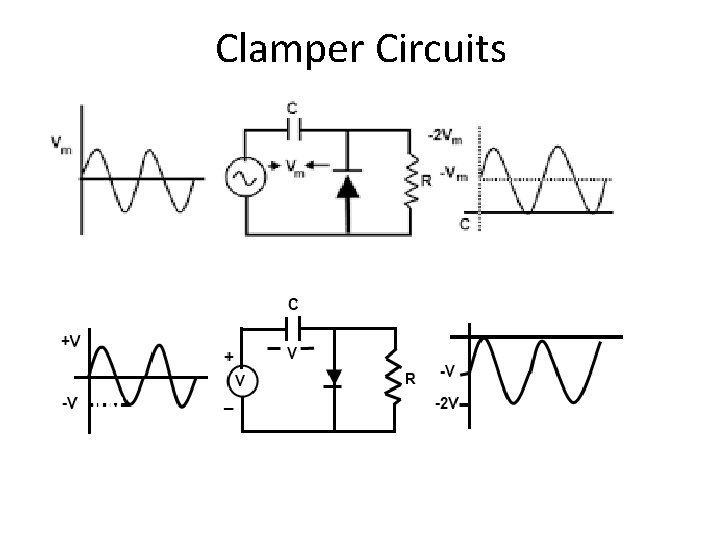
Clamper Circuits
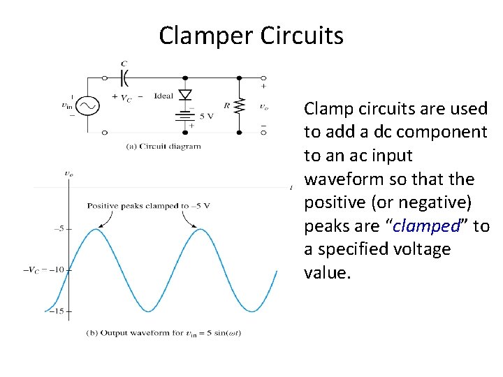
Clamper Circuits Clamp circuits are used to add a dc component to an ac input waveform so that the positive (or negative) peaks are “clamped” to a specified voltage value.
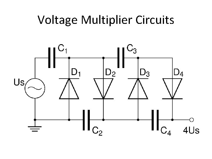
Voltage Multiplier Circuits
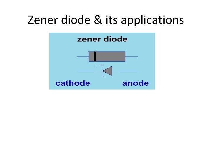
Zener diode & its applications
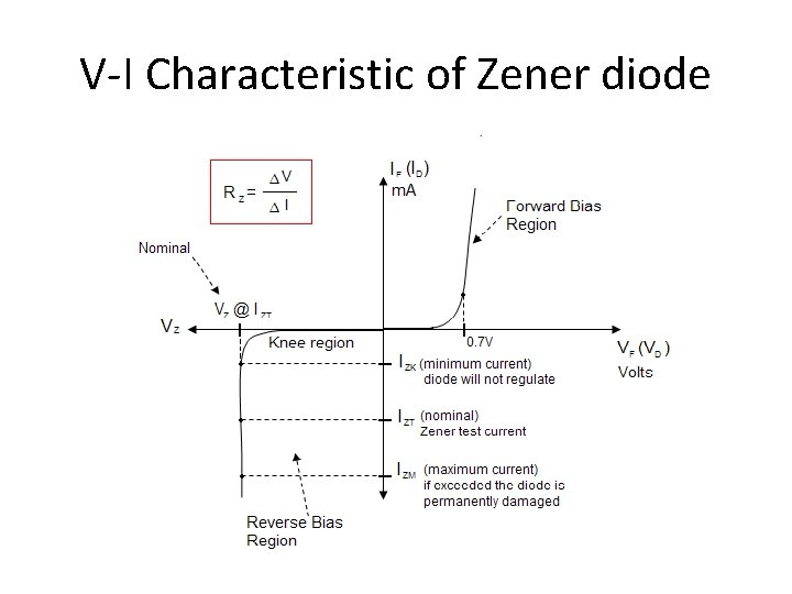
V-I Characteristic of Zener diode
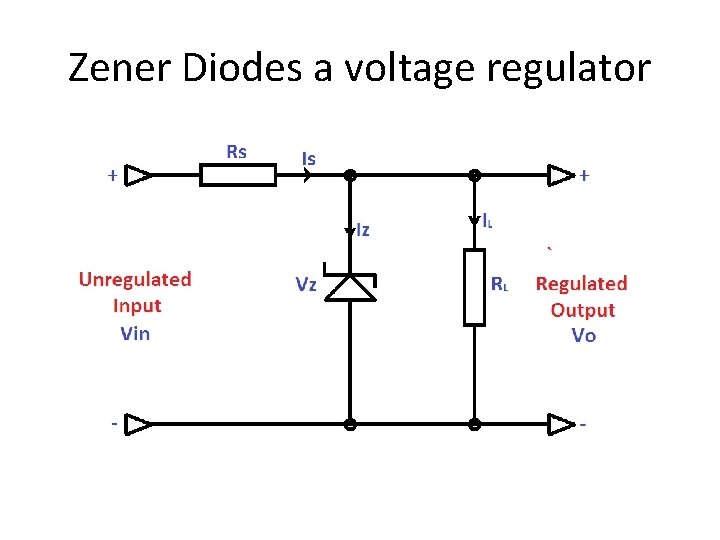
Zener Diodes a voltage regulator
Need of Regulator • The expensive electronic instruments can not use the unregulated dc power supply • They need a dc power supply whose output voltage remains constant at variation in the input voltage, load current or temperature • The power supply which provides a constant output voltage is called as a regulated power supply
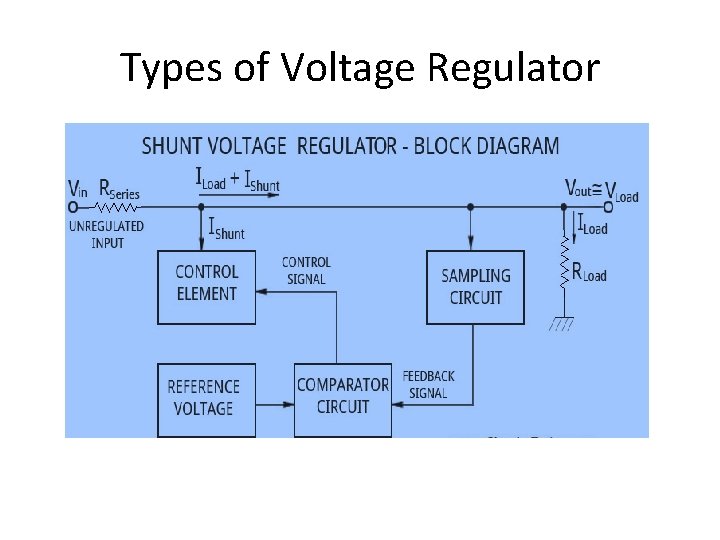
Types of Voltage Regulator
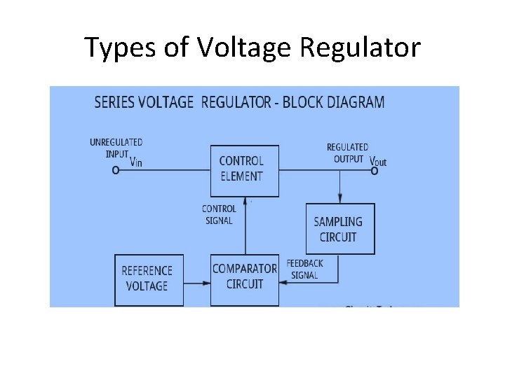
Types of Voltage Regulator
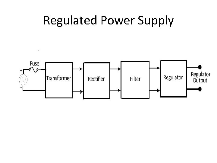
Regulated Power Supply
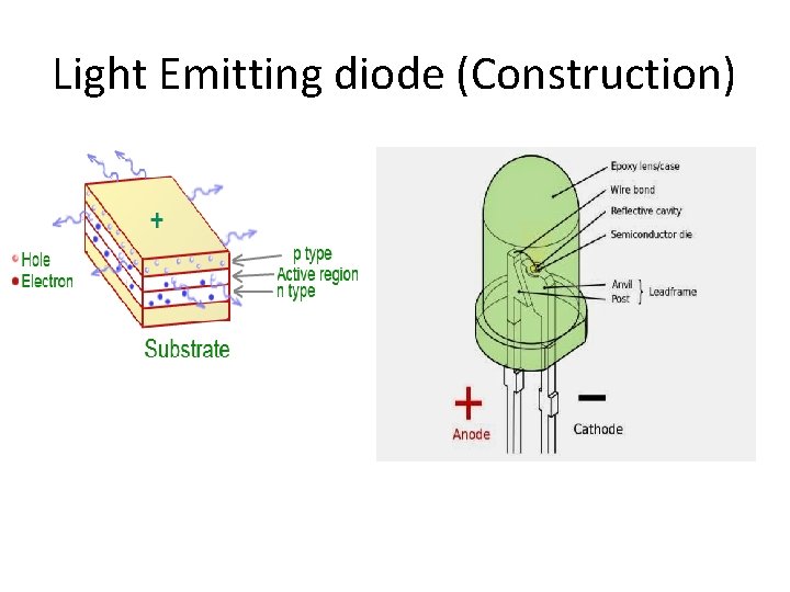
Light Emitting diode (Construction)
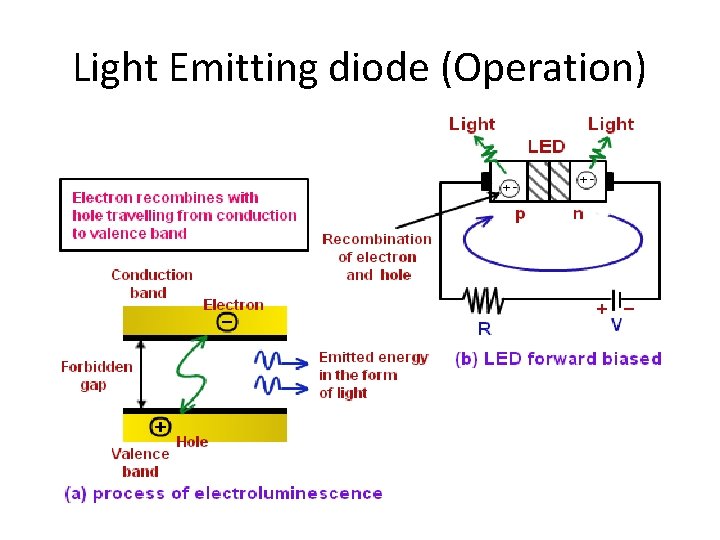
Light Emitting diode (Operation)
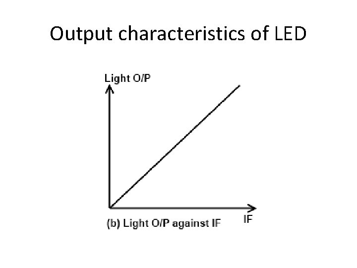
Output characteristics of LED
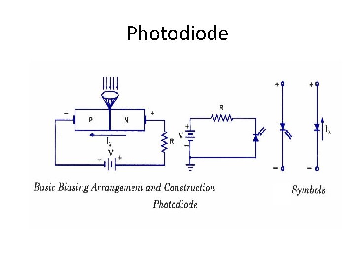
Photodiode
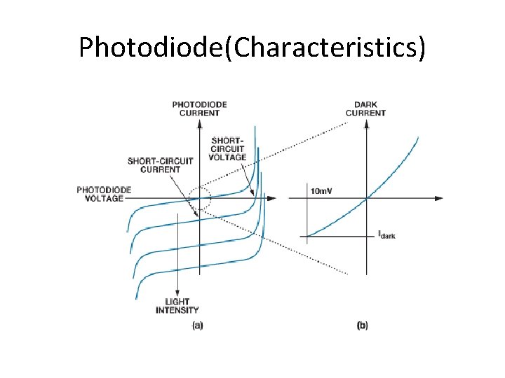
Photodiode(Characteristics)
A Presentation on Unit 2. Bipolar Junction Transistor Circuits By, ASST. PROF. P. D. JADHAV DYPIEMR, AK
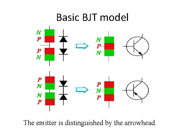
Basic BJT model The emitter is distinguished by the arrowhead.
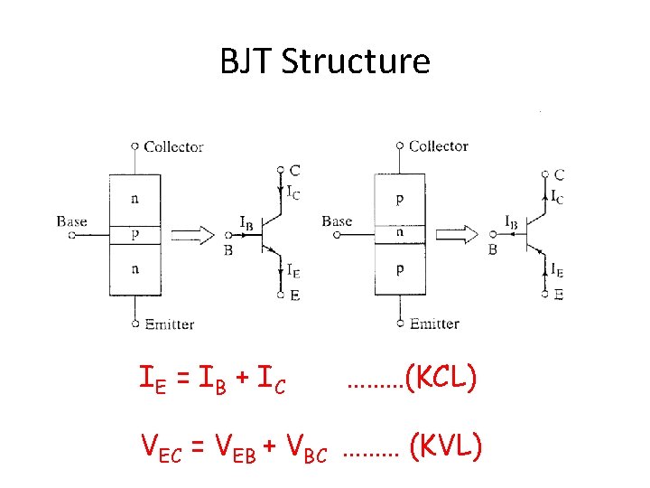
BJT Structure IE = I B + I C ………(KCL) VEC = VEB + VBC ……… (KVL)
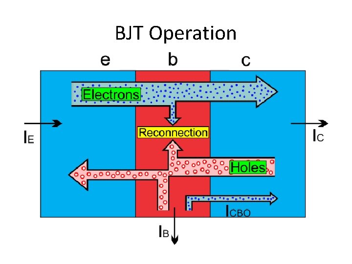
BJT Operation
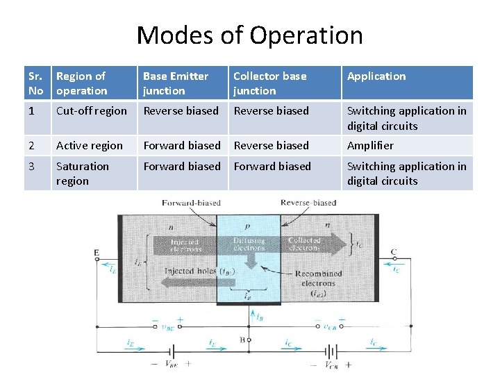
Modes of Operation Sr. No Region of operation Base Emitter junction Collector base junction Application 1 Cut-off region Reverse biased Switching application in digital circuits 2 Active region Forward biased Reverse biased Amplifier 3 Saturation region Forward biased Switching application in digital circuits
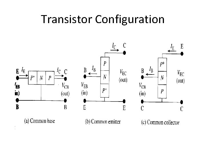
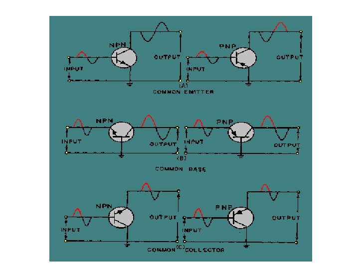
Transistor Configuration
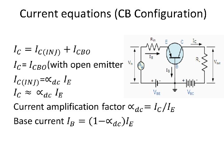
Current equations (CB Configuration) •
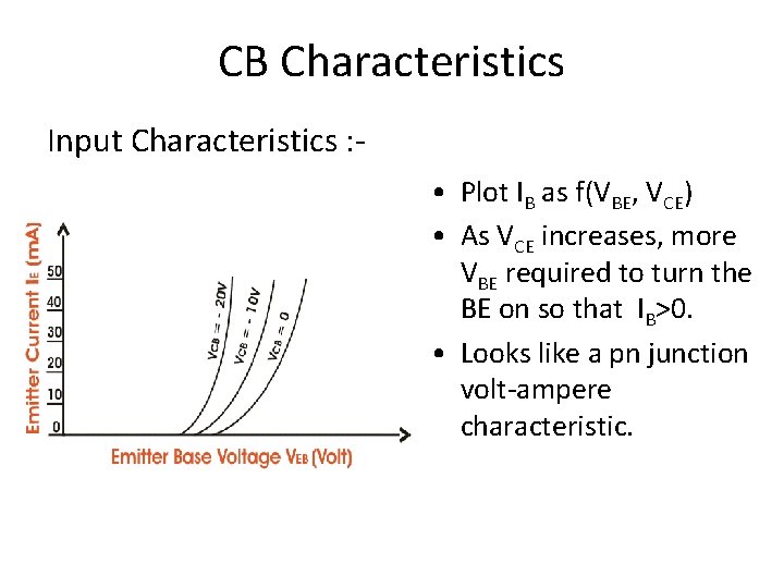
CB Characteristics Input Characteristics : • Plot IB as f(VBE, VCE) • As VCE increases, more VBE required to turn the BE on so that IB>0. • Looks like a pn junction volt-ampere characteristic.
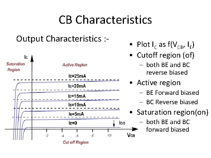
CB Characteristics Output Characteristics : - • Plot IC as f(VCB, IE) • Cutoff region (of) – both BE and BC reverse biased • Active region – BE Forward biased – BC Reverse biased • Saturation region(on) – both BE and BC forward biased
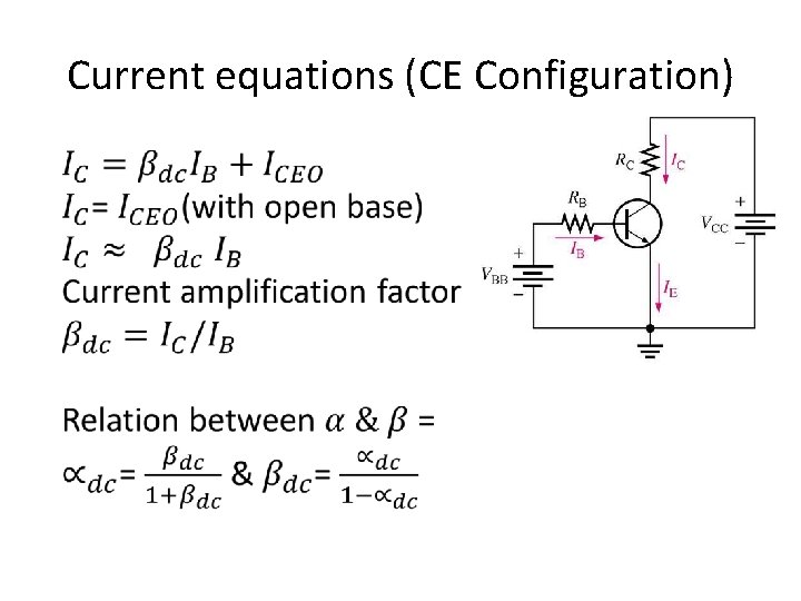
Current equations (CE Configuration)
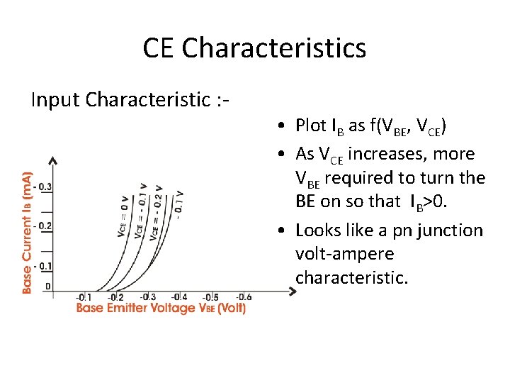
CE Characteristics Input Characteristic : - • Plot IB as f(VBE, VCE) • As VCE increases, more VBE required to turn the BE on so that IB>0. • Looks like a pn junction volt-ampere characteristic.
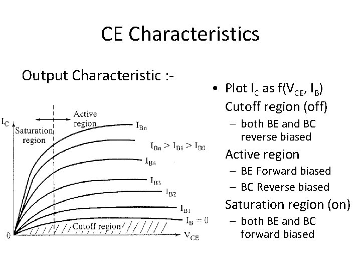
CE Characteristics Output Characteristic : - • Plot IC as f(VCE, IB) • Cutoff region (off) – both BE and BC reverse biased • Active region – BE Forward biased – BC Reverse biased • Saturation region (on) – both BE and BC forward biased
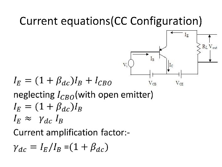
Current equations(CC Configuration) •
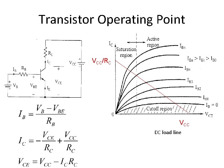
Transistor Operating Point VCC/RC VCC DC load line
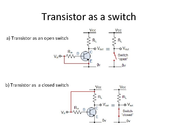
Transistor as a switch a) Transistor as an open switch b) Transistor as a closed switch
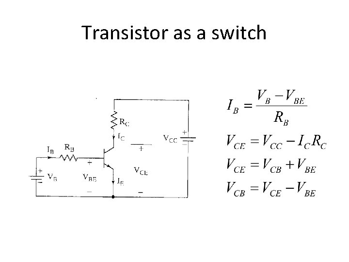
Transistor as a switch
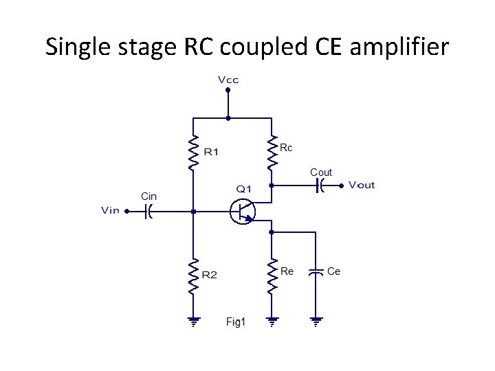
Single stage RC coupled CE amplifier
Transistor Applications • • Amplifiers Oscillators Switching circuits Logic circuits Timers & multivibrators Delay circuits Wave shaping circuits
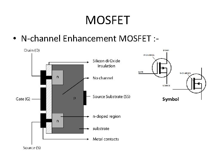
MOSFET • N-channel Enhancement MOSFET : - Symbol
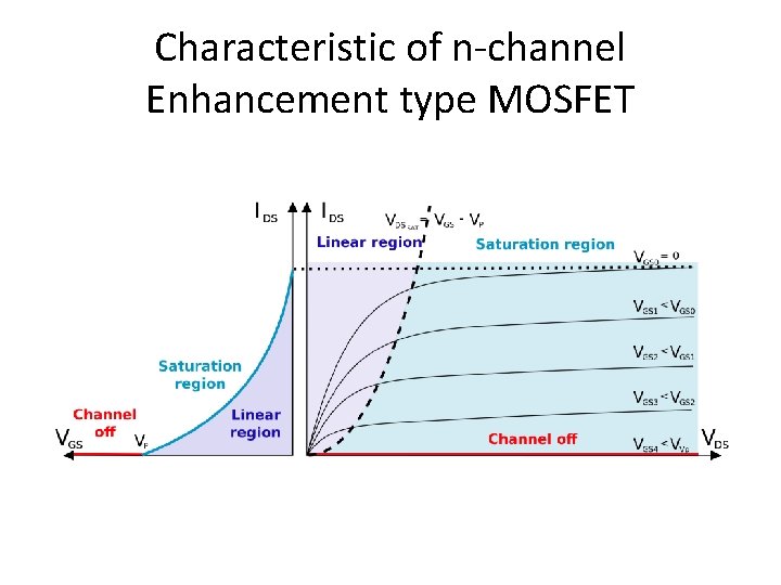
Characteristic of n-channel Enhancement type MOSFET
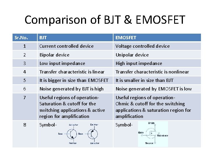
Comparison of BJT & EMOSFET Sr. No. BJT EMOSFET 1 Current controlled device Voltage controlled device 2 Bipolar device Unipolar device 3 Low input impedance High input impedance 4 Transfer characteristic is linear Transfer characteristic is nonlinear 5 It is bigger in size than EMOSFET It is smaller in size than BJT 6 Noise generated by BJT is high Noise generated by EMOSFET is low 7 Useful regions of operation. Saturation & cutoff for the switching applications & active region for amplification Useful regions of operation. Ohmic & cutoff for the switching applications & saturation region for amplification 8 Symbol-
- Slides: 55