A PCI Express Optical Link Based on LowCost
A PCI Express Optical Link Based on Low-Cost Transceiver Qualified for Radiation Hardness Andrea Triossi, Diego Barrientos, Damiano Bortolato, Roberto Isocrate, Gabriele Rampazzo, Sandro Ventura and Marco Bellato INFN – Padova and Legnaro September 18, TWEPP 2012, Oxford, UK
Outlines Backgrounds • PCI Express • LINCO Project New LINCO Boards • Block diagrams • Jitter test Radiation Tests • Transceiver comparison • PCI Express compatibility • Early Developments
Backgrounds PCI Express • • • 2. 5 -5 -8 Gbps/direction transfer rate Scalability (up to 32 lanes) Link Training Differential signaling Embedded clock (8 b/10 b) • • De-emphasis Retransmission of failed packets Quality of service PCI address space LINCO Project • Started in 2005 • Investigate a new physical medium for the protocol --> optical fibre • Manufacture copper to optical adapters • Assert their effectiveness in a harsh environment

Early development PMC form factor SFP transceivers PCI Ex / PCI bridge PCI to PCI Express optical adapter used in the VME crate of the DT sector collector (CMS) PCI / VME bridge
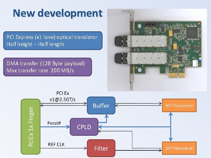
New development PCI Express (x 1 lane) optical translator Half height – Half length DMA transfer (128 Byte payload) Max transfer rate 200 MB/s

New development x 4 optical switch PCI Express Gen 2 20 Gbps Upstream port x 4 Downstream port x 1 Downstream port x 4 Two clock domains: • PCI Express spread spectrum • 100 MHz plain clock
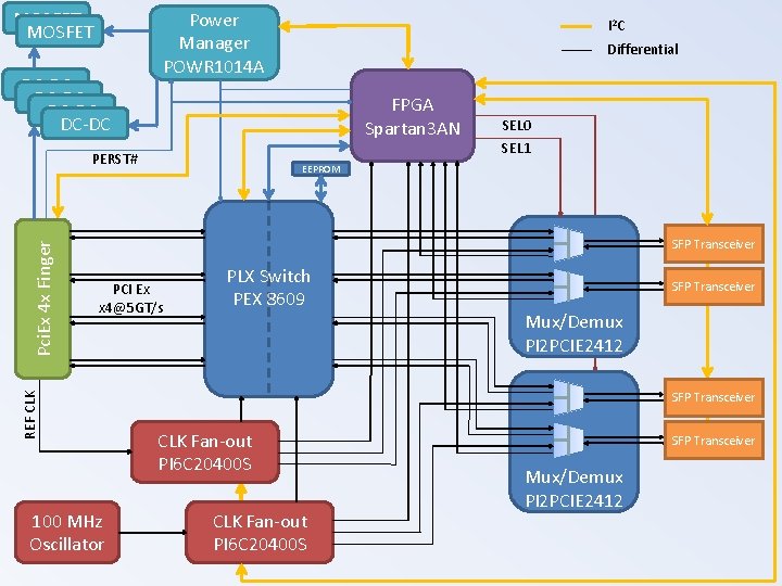
MOSFET DC-DC Power Manager POWR 1014 A Differential FPGA Spartan 3 AN PERST# SEL 0 SEL 1 EEPROM SFP Transceiver PCI Ex x 4@5 GT/s REF CLK Pci. Ex 4 x Finger I 2 C 100 MHz Oscillator PLX Switch PEX 8609 SFP Transceiver Mux/Demux PI 2 PCIE 2412 SFP Transceiver CLK Fan-out PI 6 C 20400 S SFP Transceiver Mux/Demux PI 2 PCIE 2412
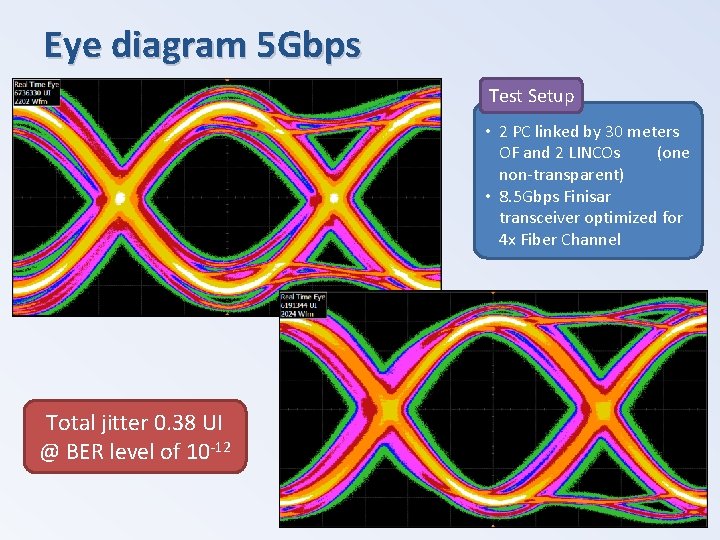
Eye diagram 5 Gbps Test Setup • 2 PC linked by 30 meters OF and 2 LINCOs (one non-transparent) • 8. 5 Gbps Finisar transceiver optimized for 4 x Fiber Channel Total jitter 0. 38 UI @ BER level of 10 -12
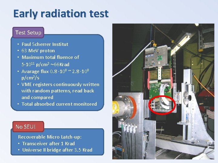
Early radiation test Test Setup • Paul Scherrer Institut • 63 Me. V proton • Maximum total fluence of 5∙ 1011 p/cm 2 ~66 Krad • Avarage flux 0. 8 ∙ 108 ~ 2. 8 ∙ 108 p/cm 2/s • VME registers continuously written with random patterns, read back and compared • Total absorbed current monitored No SEU! Recoverable Micro Latch-up: • Transceiver after 1 Krad • Universe II bridge after 3. 5 Krad
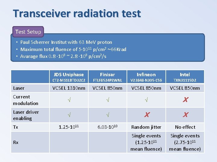
Transceiver radiation test Test Setup • Paul Scherrer Institut with 63 Me. V proton • Maximum total fluence of 5∙ 1011 p/cm 2 ~66 Krad • Avarage flux 0. 8 ∙ 108 ~ 2. 8 ∙ 108 p/cm 2/s JDS Uniphase Finisar Infineon Intel CT 2 -MS 1 LBTD 32 C 2 FTLF 8524 P 2 WNL V 23848 -N 305 -C 56 TXN 31115 D 2 VCSEL 1310 nm VCSEL 850 nm Current modulation √ √ √ X Laser driver enabling √ √ X X 1. 25∙ 1011 6. 03∙ 1010 Random jitter No effect Single events (1. 25∙ 1011 mean fluence) Single events (2. 75∙ 1011 mean fluence) Laser Tx Rx
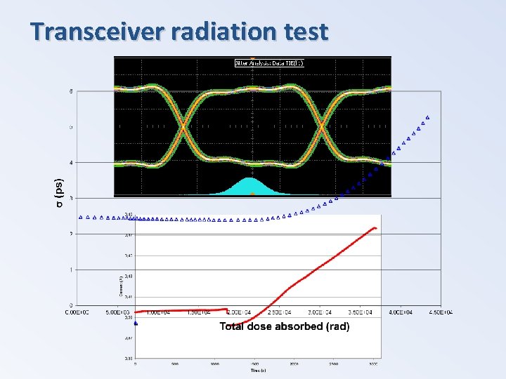
Transceiver radiation test
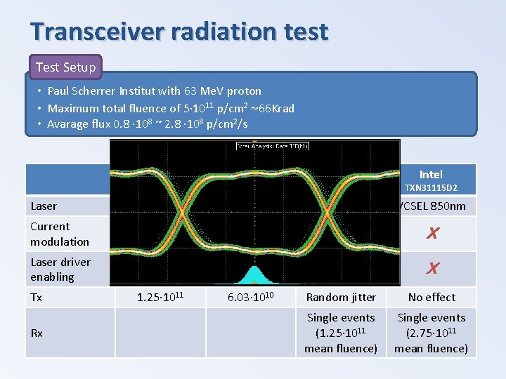
Transceiver radiation test Test Setup • Paul Scherrer Institut with 63 Me. V proton • Maximum total fluence of 5∙ 1011 p/cm 2 ~66 Krad • Avarage flux 0. 8 ∙ 108 ~ 2. 8 ∙ 108 p/cm 2/s JDS Uniphase Finisar Infineon Intel CT 2 -MS 1 LBTD 32 C 2 FTLF 8524 P 2 WNL V 23848 -N 305 -C 56 TXN 31115 D 2 VCSEL 1310 nm VCSEL 850 nm Current modulation √ √ √ X Laser driver enabling √ √ X X 1. 25∙ 1011 6. 03∙ 1010 Random jitter No effect Single events (1. 25∙ 1011 mean fluence) Single events (2. 75∙ 1011 mean fluence) Laser Tx Rx
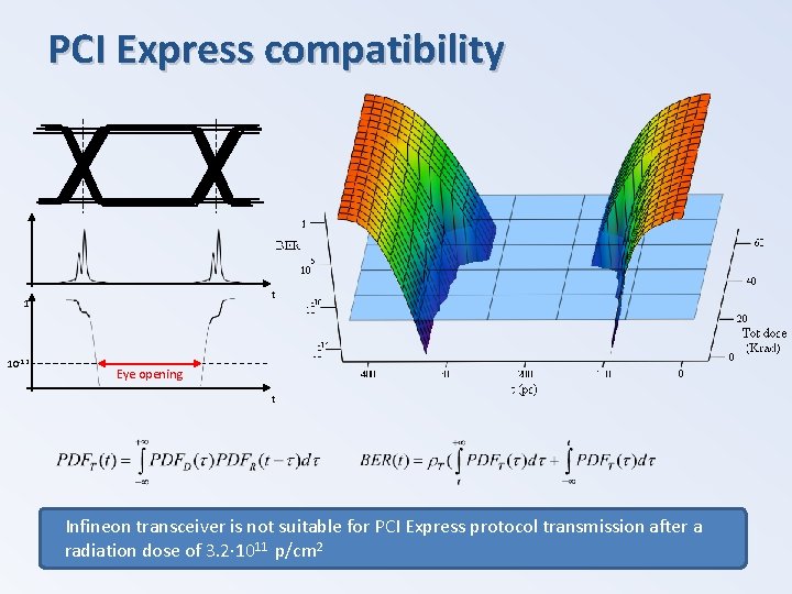
PCI Express compatibility t 1 10 -12 Eye opening t Infineon transceiver is not suitable for PCI Express protocol transmission after a radiation dose of 3. 2∙ 1011 p/cm 2
Conclusion LINCO Boards • Three flavors • Deployed in several experiments (CMS, AGATA, ICARUS…) Harsh Proton Environment • Commercial transceivers • Intel and Infineon transceivers got through CMS requirement
- Slides: 14