A new circular memory prototype for a plannar

- Slides: 1

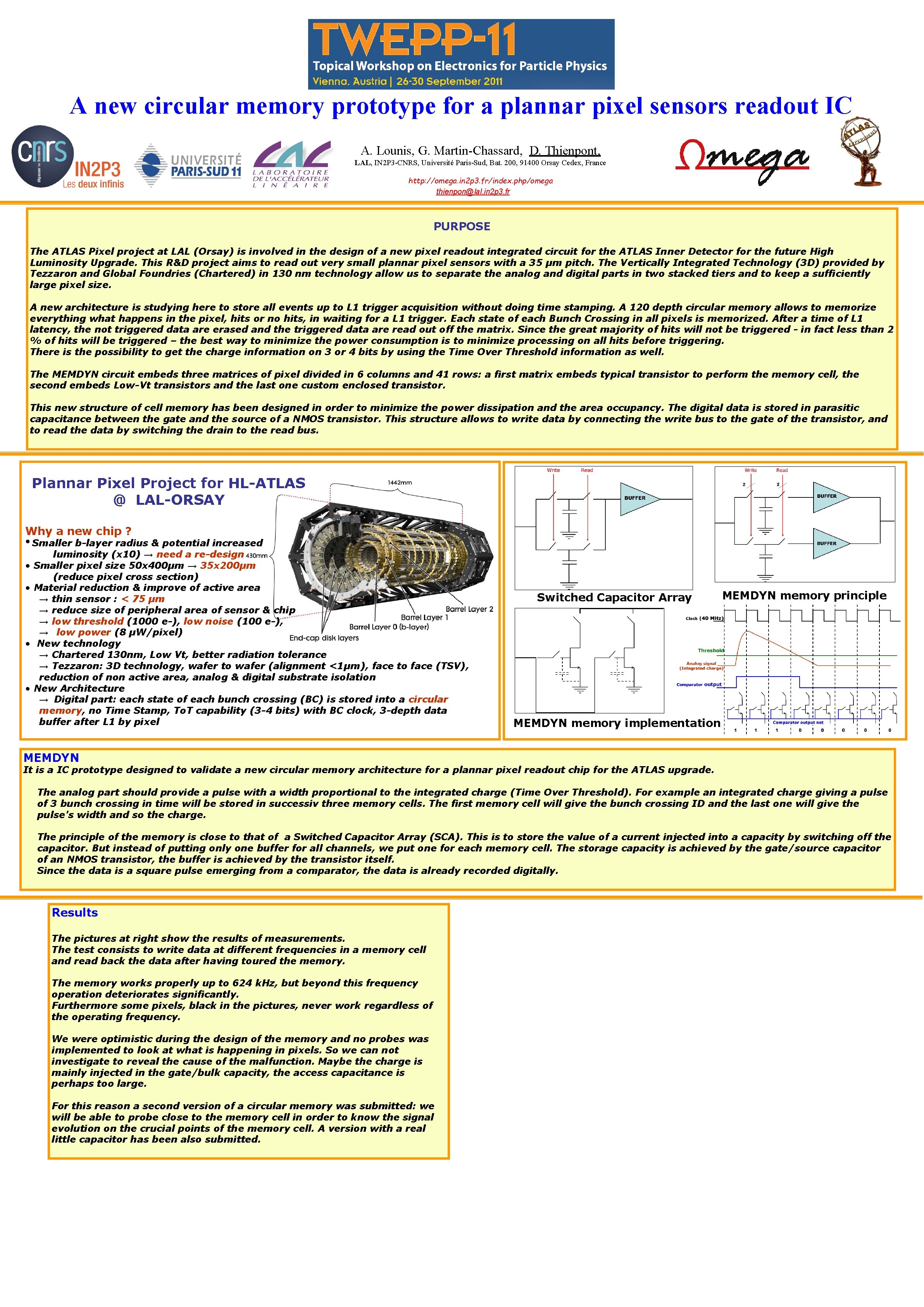
A new circular memory prototype for a plannar pixel sensors readout IC A. Lounis, G. Martin-Chassard, D. Thienpont, LAL, IN 2 P 3 -CNRS, Université Paris-Sud, Bat. 200, 91400 Orsay Cedex, France http: //omega. in 2 p 3. fr/index. php/omega thienpon@lal. in 2 p 3. fr PURPOSE The ATLAS Pixel project at LAL (Orsay) is involved in the design of a new pixel readout integrated circuit for the ATLAS Inner Detector for the future High Luminosity Upgrade. This R&D project aims to read out very small plannar pixel sensors with a 35 μm pitch. The Vertically Integrated Technology (3 D) provided by Tezzaron and Global Foundries (Chartered) in 130 nm technology allow us to separate the analog and digital parts in two stacked tiers and to keep a sufficiently large pixel size. A new architecture is studying here to store all events up to L 1 trigger acquisition without doing time stamping. A 120 depth circular memory allows to memorize everything what happens in the pixel, hits or no hits, in waiting for a L 1 trigger. Each state of each Bunch Crossing in all pixels is memorized. After a time of L 1 latency, the not triggered data are erased and the triggered data are read out off the matrix. Since the great majority of hits will not be triggered - in fact less than 2 % of hits will be triggered – the best way to minimize the power consumption is to minimize processing on all hits before triggering. There is the possibility to get the charge information on 3 or 4 bits by using the Time Over Threshold information as well. The MEMDYN circuit embeds three matrices of pixel divided in 6 columns and 41 rows: a first matrix embeds typical transistor to perform the memory cell, the second embeds Low-Vt transistors and the last one custom enclosed transistor. This new structure of cell memory has been designed in order to minimize the power dissipation and the area occupancy. The digital data is stored in parasitic capacitance between the gate and the source of a NMOS transistor. This structure allows to write data by connecting the write bus to the gate of the transistor, and to read the data by switching the drain to the read bus. Plannar Pixel Project for HL-ATLAS @ LAL-ORSAY Why a new chip ? • Smaller b-layer radius & potential increased • • luminosity (x 10) → need a re-design Smaller pixel size 50 x 400μm → 35 x 200μm (reduce pixel cross section) Material reduction & improve of active area → thin sensor : < 75 μm → reduce size of peripheral area of sensor & chip → low threshold (1000 e-), low noise (100 e-), → low power (8 μW/pixel) New technology → Chartered 130 nm, Low Vt, better radiation tolerance → Tezzaron: 3 D technology, wafer to wafer (alignment <1μm), face to face (TSV), reduction of non active area, analog & digital substrate isolation New Architecture → Digital part: each state of each bunch crossing (BC) is stored into a circular memory, no Time Stamp, To. T capability (3 -4 bits) with BC clock, 3 -depth data buffer after L 1 by pixel Switched Capacitor Array MEMDYN memory principle MEMDYN memory implementation MEMDYN It is a IC prototype designed to validate a new circular memory architecture for a plannar pixel readout chip for the ATLAS upgrade. The analog part should provide a pulse with a width proportional to the integrated charge (Time Over Threshold). For example an integrated charge giving a pulse of 3 bunch crossing in time will be stored in successiv three memory cells. The first memory cell will give the bunch crossing ID and the last one will give the pulse's width and so the charge. The principle of the memory is close to that of a Switched Capacitor Array (SCA). This is to store the value of a current injected into a capacity by switching off the capacitor. But instead of putting only one buffer for all channels, we put one for each memory cell. The storage capacity is achieved by the gate/source capacitor of an NMOS transistor, the buffer is achieved by the transistor itself. Since the data is a square pulse emerging from a comparator, the data is already recorded digitally. Results The pictures at right show the results of measurements. The test consists to write data at different frequencies in a memory cell and read back the data after having toured the memory. The memory works properly up to 624 k. Hz, but beyond this frequency operation deteriorates significantly. Furthermore some pixels, black in the pictures, never work regardless of the operating frequency. We were optimistic during the design of the memory and no probes was implemented to look at what is happening in pixels. So we can not investigate to reveal the cause of the malfunction. Maybe the charge is mainly injected in the gate/bulk capacity, the access capacitance is perhaps too large. For this reason a second version of a circular memory was submitted: we will be able to probe close to the memory cell in order to know the signal evolution on the crucial points of the memory cell. A version with a real little capacitor has been also submitted.