
A New Amplifier Shaper Discriminator for the Readout
- Slides: 1
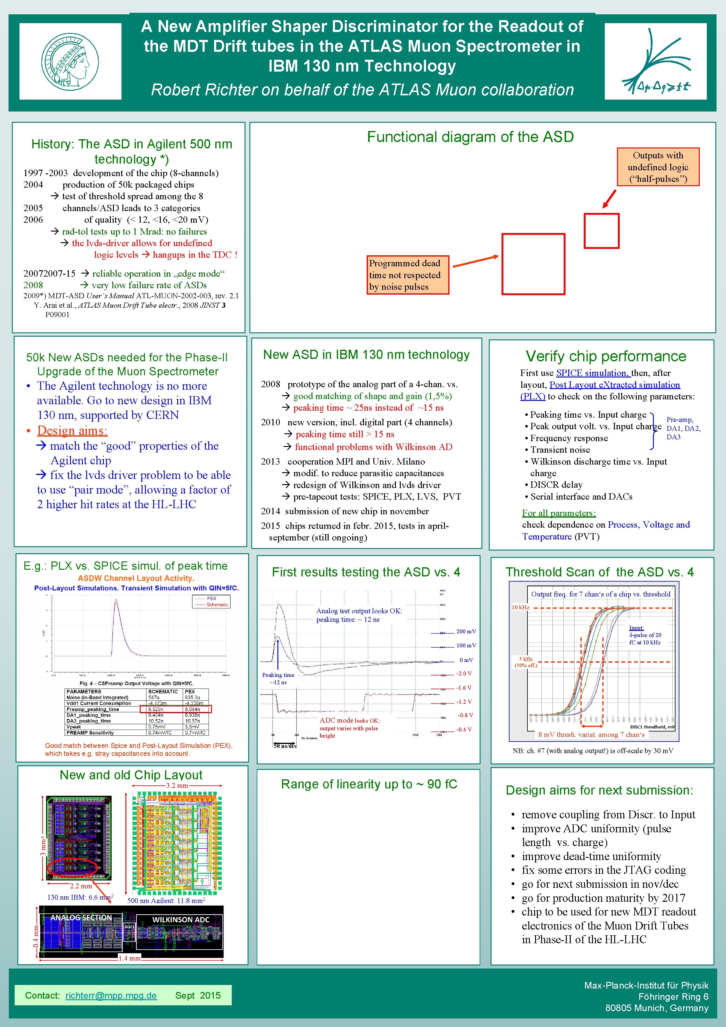
A New Amplifier Shaper Discriminator for the Readout of the MDT Drift tubes in the ATLAS Muon Spectrometer in IBM 130 nm Technology Robert Richter on behalf of the ATLAS Muon collaboration Functional diagram of the ASD History: The ASD in Agilent 500 nm technology *) Outputs with undefined logic (“half-pulses”) 1997 -2003 development of the chip (8 -channels) 2004 production of 50 k packaged chips test of threshold spread among the 8 2005 channels/ASD leads to 3 categories 2006 of quality (< 12, <16, <20 m. V) rad-tol tests up to 1 Mrad: no failures the lvds-driver allows for undefined logic levels hangups in the TDC ! Programmed dead time not respected by noise pulses 2007 -15 reliable operation in „edge mode“ 2008 very low failure rate of ASDs 2009*) MDT-ASD User’s Manual ATL-MUON-2002 -003, rev. 2. 1 Y. Arai et al. , ATLAS Muon Drift Tube electr. , 2008 JINST 3 P 09001 50 k New ASDs needed for the Phase-II Upgrade of the Muon Spectrometer New ASD in IBM 130 nm technology • The Agilent technology is no more available. Go to new design in IBM 130 nm, supported by CERN 2008 prototype of the analog part of a 4 -chan. vs. good matching of shape and gain (1, 5%) peaking time ~ 25 ns instead of ~15 ns 2010 new version, incl. digital part (4 channels) peaking time still > 15 ns functional problems with Wilkinson AD 2013 cooperation MPI and Univ. Milano modif. to reduce parasitic capacitances redesign of Wilkinson and lvds driver pre-tapeout tests: SPICE, PLX, LVS, PVT 2014 submission of new chip in november 2015 chips returned in febr. 2015, tests in aprilseptember (still ongoing) • Design aims: match the “good” properties of the Agilent chip fix the lvds driver problem to be able to use “pair mode”, allowing a factor of 2 higher hit rates at the HL-LHC E. g. : PLX vs. SPICE simul. of peak time First results testing the ASD vs. 4 Verify chip performance First use SPICE simulation, then, after layout, Post Layout e. Xtracted simulation (PLX) to check on the following parameters: • Peaking time vs. Input charge Pre-amp, • Peak output volt. vs. Input charge DA 1, DA 2, DA 3 • Frequency response • Transient noise • Wilkinson discharge time vs. Input charge • DISCR delay • Serial interface and DACs For all parameters: check dependence on Process, Voltage and Temperature (PVT) Threshold Scan of the ASD vs. 4 Output freq. for 7 chan‘s of a chip vs. threshold 10 k. Hz Analog test output looks OK: peaking time: ~ 12 ns Input: d-pulse of 20 f. C at 10 k. Hz 200 m. V 100 m. V 5 k. Hz (50% eff. ) -2. 0 V Peaking time ~12 ns -1. 6 V -1. 2 V -0. 8 V ADC mode looks OK: output varies with pulse height Good match between Spice and Post-Layout Simulation (PEX), which takes e. g. stray capacitances into account. New and old Chip Layout 3 mm 3. 2 mm ~2, 2 mm mm 2. 2 500 nm Agilent: 11. 8 mm 2 0. 40. 38 mm mm 130 nm IBM: 6. 6 mm 2 -0. 4 V 50 ns/div Range of linearity up to ~ 90 f. C 8 m. V thresh. variat. among 7 chan‘s NB: ch. #7 (with analog output!) is off-scale by 30 m. V Design aims for next submission: • remove coupling from Discr. to Input • improve ADC uniformity (pulse length vs. charge) • improve dead-time uniformity • fix some errors in the JTAG coding • go for next submission in nov/dec • go for production maturity by 2017 • chip to be used for new MDT readout electronics of the Muon Drift Tubes in Phase-II of the HL-LHC 1. 4 mm Contact: richterr@mpp. mpg. de Sept 2015 Max-Planck-Institut für Physik Föhringer Ring 6 80805 Munich, Germany