A MixedSignal CMOS VLSI Image Convolution Circuit using


![Signal-Noise Ratio 10 Log [ sij 2/ (yij – sij)2] Space Based SNR |x[n]|2 Signal-Noise Ratio 10 Log [ sij 2/ (yij – sij)2] Space Based SNR |x[n]|2](https://slidetodoc.com/presentation_image_h/9a7e9f084376f3eba63b41c06e628f20/image-8.jpg)



- Slides: 24

A Mixed-Signal CMOS VLSI Image Convolution Circuit using Error Spectrum Shaping Brent Buchanan July 2001 School of Electrical and Computer Engineering Georgia Institute of Technology

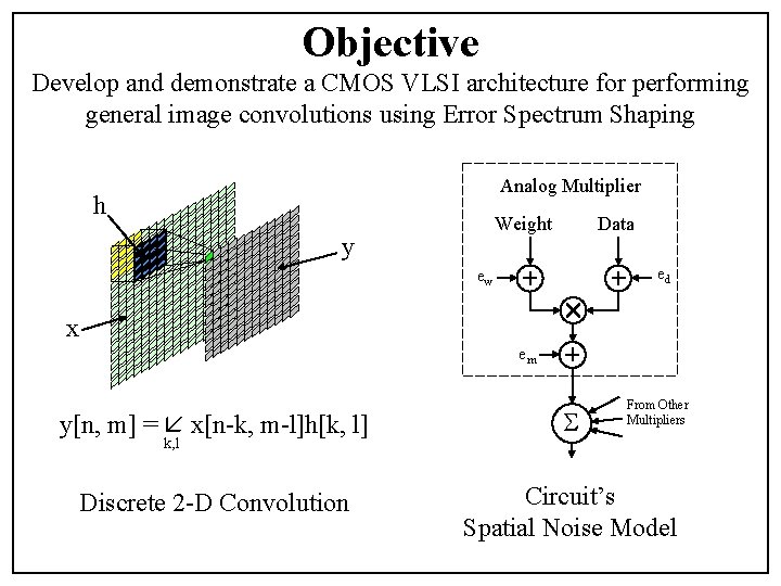
Objective Develop and demonstrate a CMOS VLSI architecture for performing general image convolutions using Error Spectrum Shaping Analog Multiplier h Weight y Data ed ew x em From Other Multipliers y[n, m] = x[n-k, m-l]h[k, l] S Discrete 2 -D Convolution Circuit’s Spatial Noise Model k, l

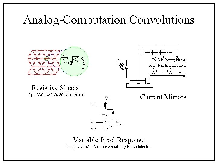
Analog-Computation Convolutions To Neighboring Pixels From Neighboring Pixels Iout Resistive Sheets E. g. , Mahowald’s Silicon Retina Current Mirrors Variable Pixel Response E. g. , Funatsu’s Variable Sensitivity Photodetectors

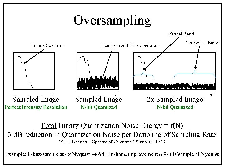
Oversampling Signal Band Image Spectrum p Quantization Noise Spectrum p ‘Disposal’ Band Sampled Image 2 x Sampled Image Perfect Intensity Resolution N-bit Quantized p Total Binary Quantization Noise Energy = f(N) 3 d. B reduction in Quantization Noise per Doubling of Sampling Rate W. R. Bennett, “Spectra of Quantized Signals, ” 1948 Example: 8 -bits/sample at 4 x Nyquist 6 d. B in-band improvement 9 -bits/sample at Nyquist

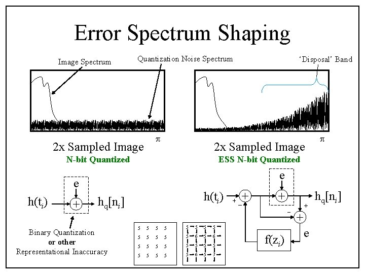
Error Spectrum Shaping Image Spectrum Quantization Noise Spectrum p 2 x Sampled Image N-bit Quantized p ESS N-bit Quantized e e h(ti) ‘Disposal’ Band Binary Quantization or other Representational Inaccuracy hq[ni] h(ti) hq[ni] 5 5 5 5 5 5 5 6 5 7 f(zi) e

Convolution and Noise Model Analog Multiplier Weight Data ed ew em From Other Multipliers y[n, m] = x[n-k, m-l]h[k, l] S Discrete 2 -D Convolution Circuit’s Spatial Noise Model k, l

Quantization Examples 5122 x 1 -bit Simple Quantization ESS Quantization
![SignalNoise Ratio 10 Log sij 2 yij sij2 Space Based SNR xn2 Signal-Noise Ratio 10 Log [ sij 2/ (yij – sij)2] Space Based SNR |x[n]|2](https://slidetodoc.com/presentation_image_h/9a7e9f084376f3eba63b41c06e628f20/image-8.jpg)
Signal-Noise Ratio 10 Log [ sij 2/ (yij – sij)2] Space Based SNR |x[n]|2 = 1/N |X(n)|2 Parseval’s Relation 10 Log [ |Sij|2 / |Yij – Sij|2] Spectrum Based SNR Total in-band noise (d. B) vs signal bandwidth 3 -bit Lenna 5122, 10242, 20482 images Binary Quantization Noise

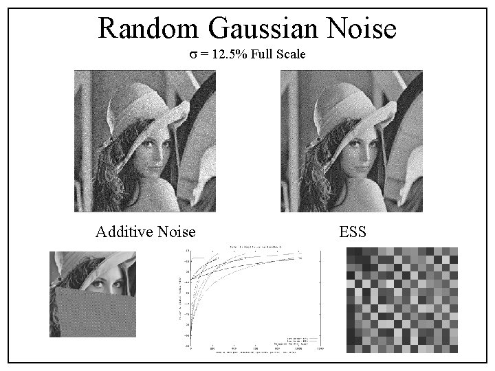
Random Gaussian Noise s = 12. 5% Full Scale Additive Noise ESS

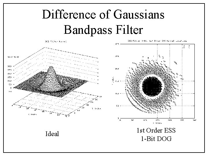
Difference of Gaussians Bandpass Filter Ideal 1 st Order ESS 1 -Bit DOG

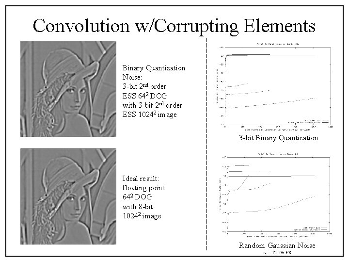
Convolution w/Corrupting Elements Binary Quantization Noise: 3 -bit 2 nd order ESS 642 DOG with 3 -bit 2 nd order ESS 10242 image 3 -bit Binary Quantization Ideal result: floating point 642 DOG with 8 -bit 10242 image Random Gaussian Noise s = 12. 5% FS

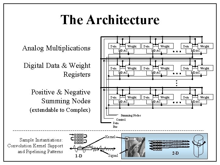
The Architecture Analog Multiplications Digital Data & Weight Registers Positive & Negative Summing Nodes Data Weight MDAC Data Weight MDAC Data Weight MDAC (extendable to Complex) Summing Nodes Control Data Bus Sample Instantiations: Convolution Kernel Support and Pipelining Patterns Kernel 1 -D Signal 2 -D

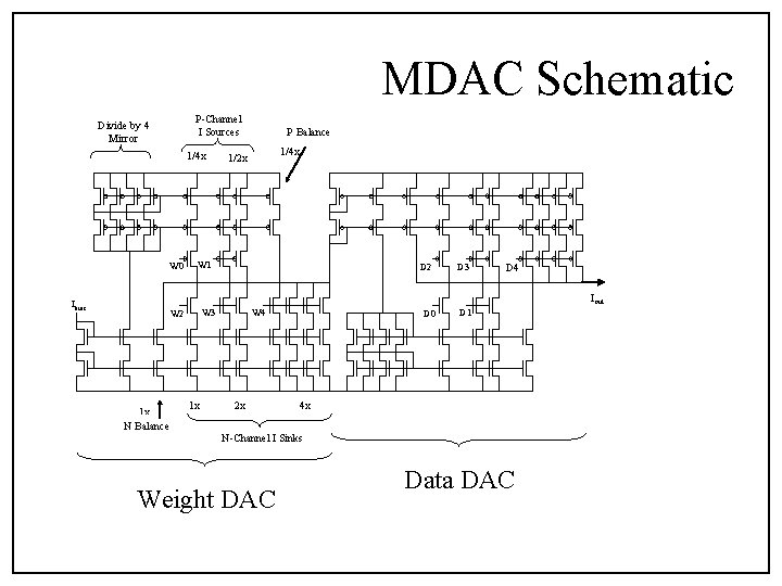
MDAC Schematic P-Channel I Sources Divide by 4 Mirror 1/4 x W 0 P Balance 1/4 x 1/2 x W 1 D 2 D 3 D 4 Iout Ibias W 3 W 2 1 x N Balance 1 x W 4 2 x D 0 D 1 4 x N-Channel I Sinks Weight DAC Data DAC

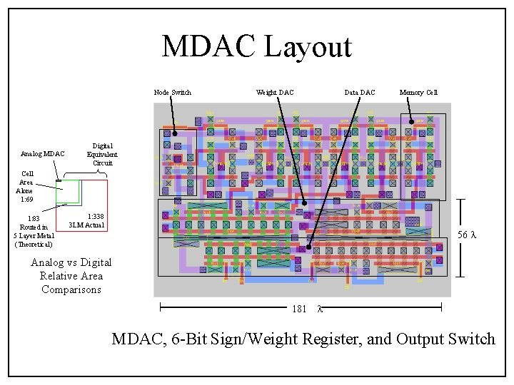
MDAC Layout Node Switch Analog MDAC Weight DAC Data DAC Memory Cell Digital Equivalent Circuit Cell Area Alone 1: 69 1: 83 Routed in 5 Layer Metal (Theoretical) 1: 338 3 LM Actual 56 l Analog vs Digital Relative Area Comparisons 181 l MDAC, 6 -Bit Sign/Weight Register, and Output Switch

Measured Results I: Single MDAC Chip #8, MDAC at Row 0 Column 0

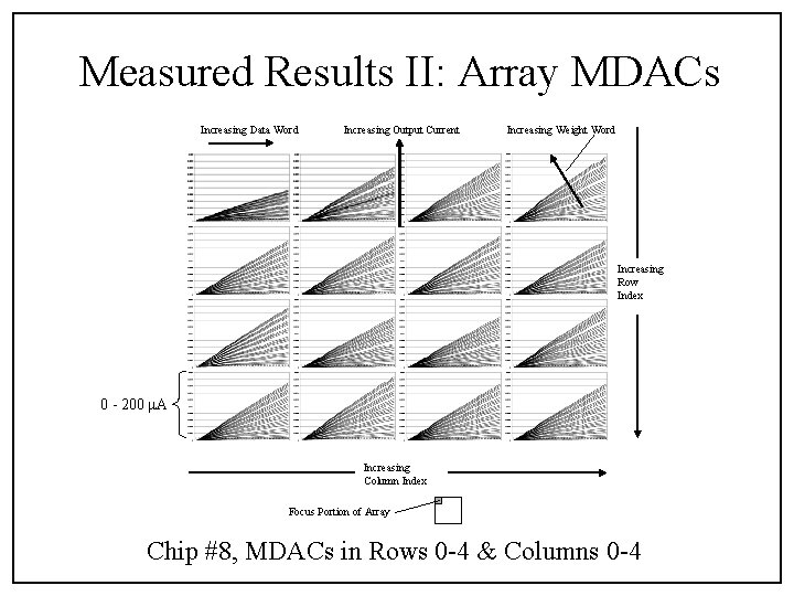
Measured Results II: Array MDACs Increasing Data Word Increasing Output Current Increasing Weight Word Increasing Row Index 0 - 200 m. A Increasing Column Index Focus Portion of Array Chip #8, MDACs in Rows 0 -4 & Columns 0 -4

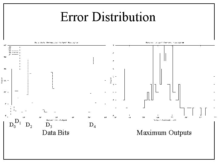
Error Distribution D D 0 1 D 2 D 3 Data Bits D 4 Maximum Outputs

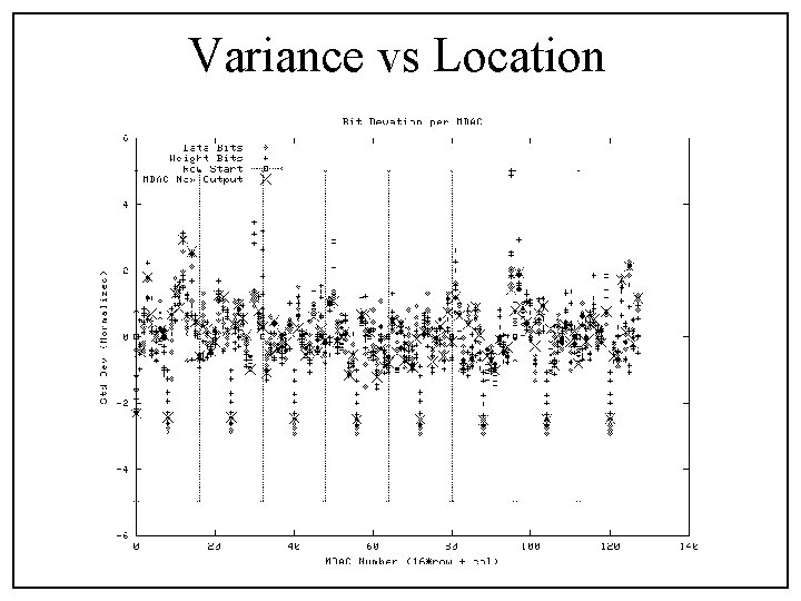
Variance vs Location

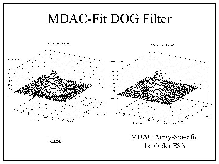
MDAC-Fit DOG Filter Ideal MDAC Array-Specific 1 st Order ESS

DOG Convolution Results Ideal result: floating point 642 DOG convolved with the 8 -bit 10242 image MDAC-based result: 642 MDAC array-specific 1 st order ESS DOG convolved with 10242 1 -bit 1 st order ESS image

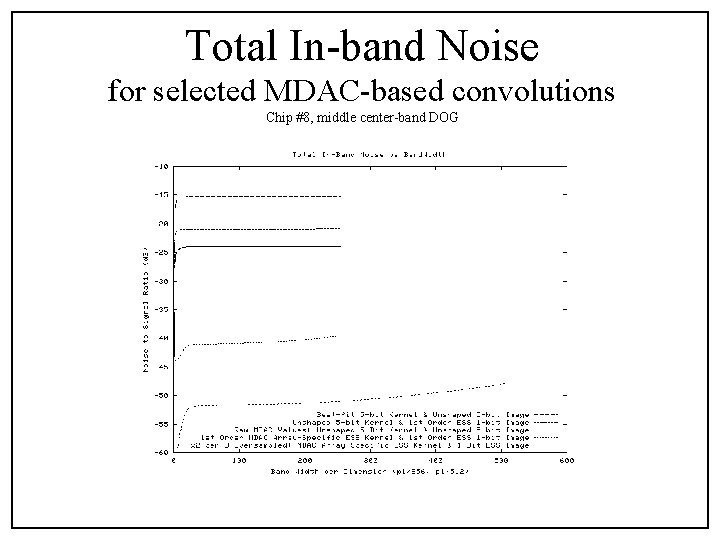
Total In-band Noise for selected MDAC-based convolutions Chip #8, middle center-band DOG

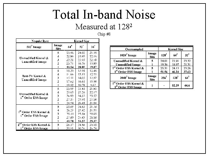
Total In-band Noise Measured at 1282 Chip #8

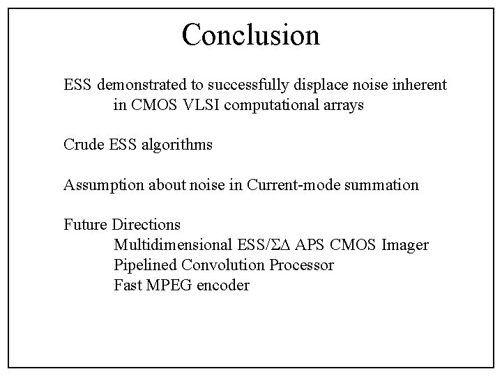
Conclusion ESS demonstrated to successfully displace noise inherent in CMOS VLSI computational arrays Crude ESS algorithms Assumption about noise in Current-mode summation Future Directions Multidimensional ESS/SD APS CMOS Imager Pipelined Convolution Processor Fast MPEG encoder

THESIS RELATED Publications B. Buchanan, M. Brooke, “ Error Spectrum Shaping in Analog Image Convolution Circuits“, Submitted to IEEE Transactions on Circuits and Systems I: Fundamental Theory and Applications B. Buchanan, M. Brooke, “A Mixed-Signal Image Convolution Circuit using Error Spectrum Shaping “, Submitted to IEEE Transactions on Circuits and Systems II: Analog and Digital Signal Processing B. Buchanan, M. Brooke, “Analog CMOS Image Convolution Circuitry using Error Spectrum Shaping, ” Proceedings of Philips Research 10 th Seminar on Analogue and Mixed-Signal Design, Eindhoven, Netherlands, June 2001 OTHER B. Buchanan, “IC Cell and Library Identification”, Application for United States Letters Patent, Filed 29 June 2001 B. Buchanan, V. Madisetti, M. Brooke, "Performance of a Fast Analog VLSI Implementation of the DFT", Proceedings of the 35 th Midwest Symposium on Circuits and Systems, Vol 2, pp 1353 -6, August 1992 B. Buchanan, C. Camperi-Ginestet, T. Morris, M. Brooke, S. De. Weerth, N. Jokerst, M. Allen, "High Density Focal Plane Signal Processing Using 3 -D Vertical Interconnects", Proceedings of the 37 th Midwest Symposium on Circuits and Systems, vol 1, pp 191 -4, Aug 1994 C. Camperi-Ginestet, B. Buchanan, Y. Wang, N. Jokerst, M. Brooke, M. Allen, "Three Dimensional Smart Pixel Integration of a Ga. As-Based Detector Array Directly on Top of Silicon Circuits", LEOS Summer Topical Meetings 1994: Smart Pixels, pp 56 -8, July 1994 C. Camperi-Ginestet, B. Buchanan, S. Wilkinson, N. Jokerst, M. Brooke, "Integration of In. P-Based Thin Film Emitters and Detectors Onto a Single Silicon Circuit", Optical Society of America 1995 Spring Topical Meetings , March 1995, Salt Lake City, Utah D. S. Wills, W. S. Lacy, C. Camperi-Ginestet, B. Buchanan, H. H. Cat, S. T. Wilkinson, M. Lee, N. M. Jokerst, M. Brooke, "A Three-Dimensional High. Throughput Archtecture Using Through-Wafer Optical Interconnect", IEEE-OSA J. L. T. , vol 13, pp 1085 -92, June 1995 J. Cross, A. Lopez-Lagunas, B. Buchanan, L. Carastro, S. C. Wang, N. M. Jokerst, S. Wills, M. Brooke, M. A. Ingram "A Single-Fiber Bidirectional Optical Link Using Colocated Emitters and Detectors", IEEE Photon. Tech. Lett. , vol 8, no 10, pp 1385 -7, Oct 1996 N. M. Jokerst, M. Brooke, O. Vendier, S. T. Wilkinson, S. M. Fike, M. Lee, B. Buchanan, D. S. Wills, A. Brown, "Manufacturable Mult-Material Integration Compond Semiconductor Devices Bonded to Silicon Circuitry", SPIE, 1995 N. M. Jokerst, M. Brooke, O. Vendier, S. T. Wilkinson, S. M. Fike, M. Lee, E. Twyford, J. Cross, B. Buchanan, D. S. Wills, "Thin Film Mult-Material Optoelectronic Integrated Circuits", IEEE Trans. on Comp. Pack. and Man. Tech. Part B. , vol 19, no 1 pp. 97 -106, Feb 1996 N. M. Jokerst, C. Camperi-Ginestet, B. Buchanan, S. T. Wilkinson, M. Brooke, "Communication Through Stacked Silicon Circuitry Using Integratged Thin Film In. P-based Emitters and Detectors", IEEE Photon. Tech. Lett. , vol 7, pp 1028 -30, Sept 1995 S. M. Fike, B. Buchanan, N. Jokerst, M. Brooke, T. Morris, S. De. Weerth, "8 x 8 Array of Thin-Film Photodetectors Vertically Electrically Interconnected to Silicon Circuitry", IEEE Photon. Tech. Lett. , vo 7, no 10, Oct 1995 W. S. Lacy, C. Camperi-Ginestet, B. Buchanan, M. Lee, S. Wilkinson, D. S. Wills, N. M. Jokerst, M. Brooke, "A Fine-Grain, High-Throughput Architecture Using Through-Wafer Optical Interconnect", Special Issue of the Journal of Light. Tech. , Jan 1995 W. S. Lacy, M. Grossglauser, C. Camperi-Ginestet, B. Buchanan, D. S. Wills, N. M. Jokerst, M. Brooke, "A Fine-Grain, High-Throughput Architecture Using Through-Wafer Optical Interconnect", Proceedings of: Workshop on Massively Parallel Processing Using Optical Interconnections, April 1994, Cancun, Mexico