A Low Power SRAM Design Caroline Andrews Robert
A Low Power SRAM Design Caroline Andrews Robert Hunter Yousef Shakhsheer December 6 th, 2007
Purpose • Develop a functioning SRAM memory device • Implement design features to reduce overall power consumption • Design a robust memory device that operates over a large range of temperatures, voltages, and process corners
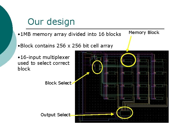
Our design • 1 MB memory array divided into 16 blocks • Block contains 256 x 256 bit cell array • 16 -input multiplexer used to select correct block Block Select Output Select Memory Block
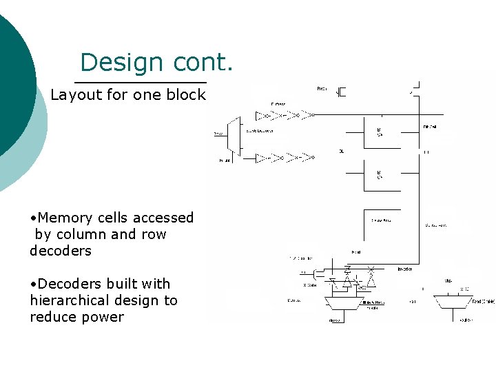
Design cont. Layout for one block • Memory cells accessed by column and row decoders • Decoders built with hierarchical design to reduce power
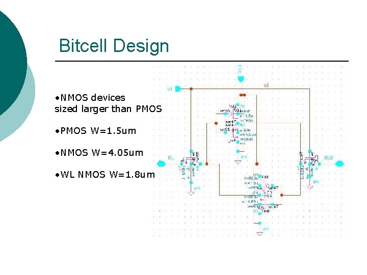
Bitcell Design • NMOS devices sized larger than PMOS • PMOS W=1. 5 um • NMOS W=4. 05 um • WL NMOS W=1. 8 um
Special Features Enable signals are distributed throughout the memory periphery • Allow for a considerable reduction in power • Only one memory block is active at any time • Sense amplifiers enabled only during read When read or write are not asserted, entire periphery is disabled
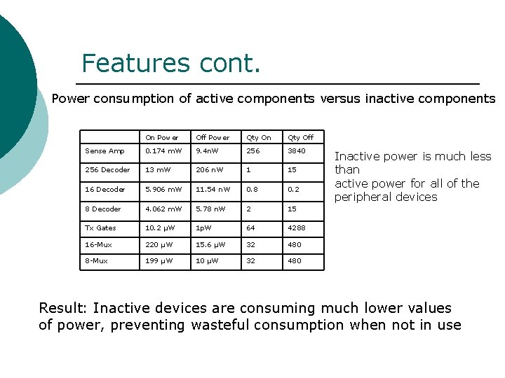
Features cont. Power consumption of active components versus inactive components On Power Off Power Qty On Qty Off Sense Amp 0. 174 m. W 9. 4 n. W 256 3840 256 Decoder 13 m. W 206 n. W 1 15 16 Decoder 5. 906 m. W 11. 54 n. W 0. 8 0. 2 8 Decoder 4. 062 m. W 5. 78 n. W 2 15 Tx Gates 10. 2 μW 1 p. W 64 4288 16 -Mux 220 μW 15. 6 μW 32 480 8 -Mux 199 μW 10 μW 32 480 Inactive power is much less than active power for all of the peripheral devices Result: Inactive devices are consuming much lower values of power, preventing wasteful consumption when not in use
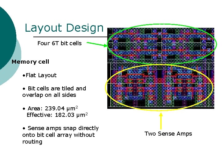
Layout Design Four 6 T bit cells Memory cell • Flat Layout • Bit cells are tiled and overlap on all sides • Area: 239. 04 μm 2 Effective: 182. 03 μm 2 • Sense amps snap directly onto bit cell array without routing Two Sense Amps
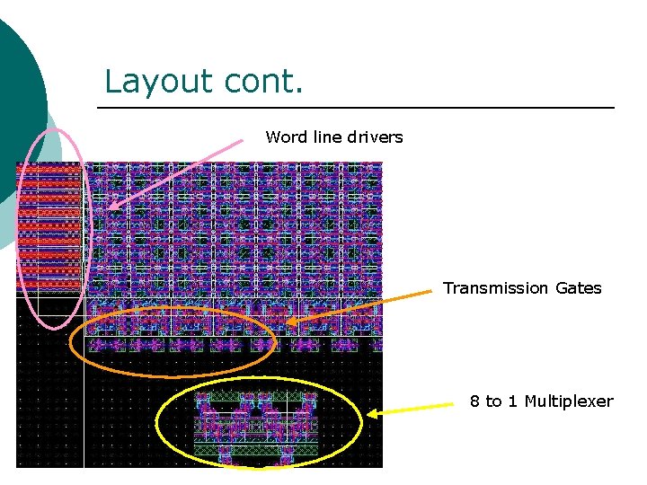
Layout cont. Word line drivers Transmission Gates 8 to 1 Multiplexer
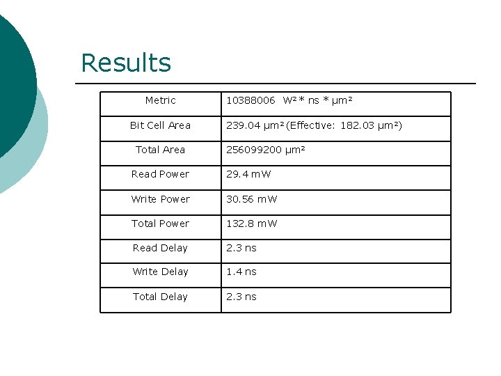
Results Metric Bit Cell Area Total Area 10388006 W 2 * ns * μm 2 239. 04 μm 2 (Effective: 182. 03 μm 2) 256099200 μm 2 Read Power 29. 4 m. W Write Power 30. 56 m. W Total Power 132. 8 m. W Read Delay 2. 3 ns Write Delay 1. 4 ns Total Delay 2. 3 ns
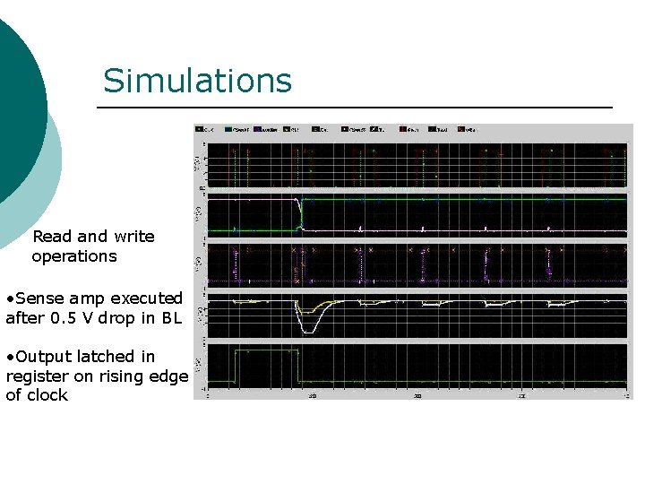
Simulations Read and write operations • Sense amp executed after 0. 5 V drop in BL • Output latched in register on rising edge of clock
Simulations cont. Memory Block simulated at all voltages, temperatures, and process corners • V(4. 5, 5, 5. 5) T(0 C, 27 C, 50 C) P(TT, FF, SS, SF, FS) • Done for 1 bit Read and Write Memory Block also simulated under 32 -bit Read and Write
Summary Memory blocked successfully designed and simulated under variety of conditions Power consumption is minimized with enable signals on memory periphery Area is minimized with overlapping bitcells and sense amplifiers Further development could result in more power savings

Questions?
- Slides: 14