A highPrecision Timing ASIC for TOFPET Applications Pierpaolo





- Slides: 38

A high-Precision Timing ASIC for TOF-PET Applications Pierpaolo Valerio on behalf of the TT-PET collaboration

Outline The TT-PET scanner Front-end architecture System integration Prototype measurements Next steps and conclusions P. Valerio - pierpaolo. valerio@unige. ch 13 -Sep-17 2

Outline The TT-PET scanner Front-end architecture System integration Prototype measurements Next steps and conclusions P. Valerio - pierpaolo. valerio@unige. ch 13 -Sep-17 3

The TT-PET collaboration A 3 -yer project to produce a PET Scanner for small animals based on silicon detector technology, insertable in an MRI machine and with 30 ps RMS time resolution. The project started in March 2016. Collaborating institutes: University of Geneva Front End Electronics and detector design University of Bern Hôpital cantonale de Genève INFN of Roma Tor Vergata Front End Electronics and detector design CERN Stanford University P. Valerio - pierpaolo. valerio@unige. ch 13 -Sep-17 4

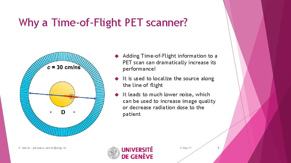
Why a Time-of-Flight PET scanner? P. Valerio - pierpaolo. valerio@unige. ch Adding Time-of-Flight information to a PET scan dramatically increase its performance! It is used to localize the source along the line of flight It leads to much lower noise, which can be used to increase image quality or decrease radiation dose to the patient 13 -Sep-17 5

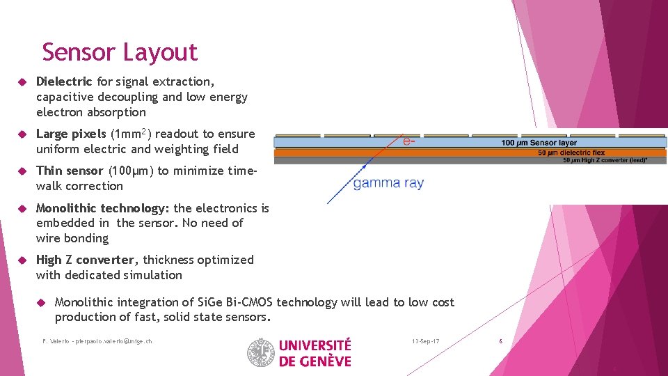
Sensor Layout Dielectric for signal extraction, capacitive decoupling and low energy electron absorption Large pixels (1 mm 2) readout to ensure uniform electric and weighting field Thin sensor (100µm) to minimize timewalk correction Monolithic technology: the electronics is embedded in the sensor. No need of wire bonding High Z converter, thickness optimized with dedicated simulation Monolithic integration of Si. Ge Bi-CMOS technology will lead to low cost production of fast, solid state sensors. P. Valerio - pierpaolo. valerio@unige. ch 13 -Sep-17 6 6

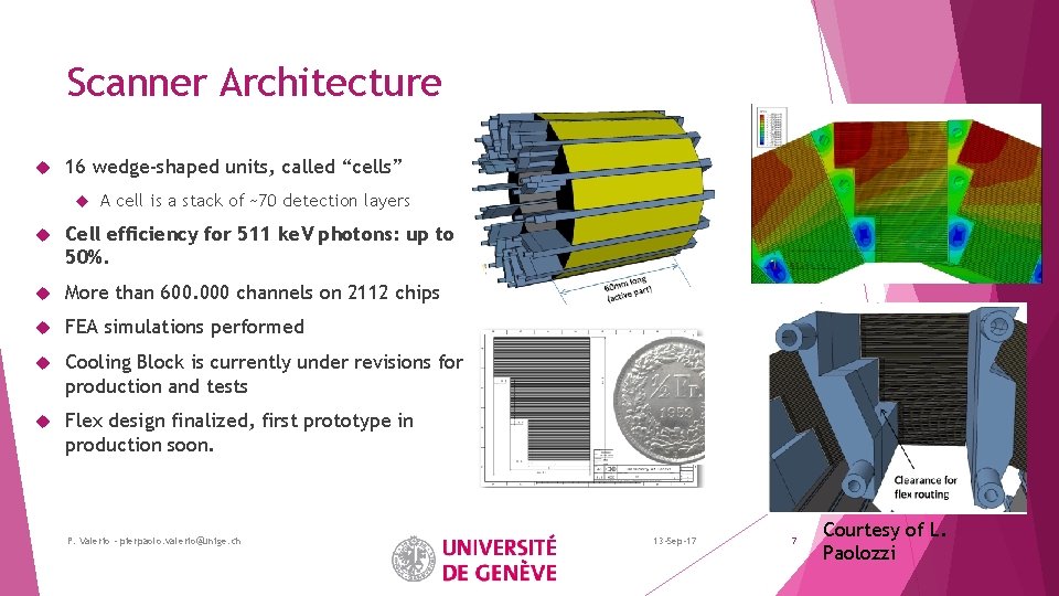
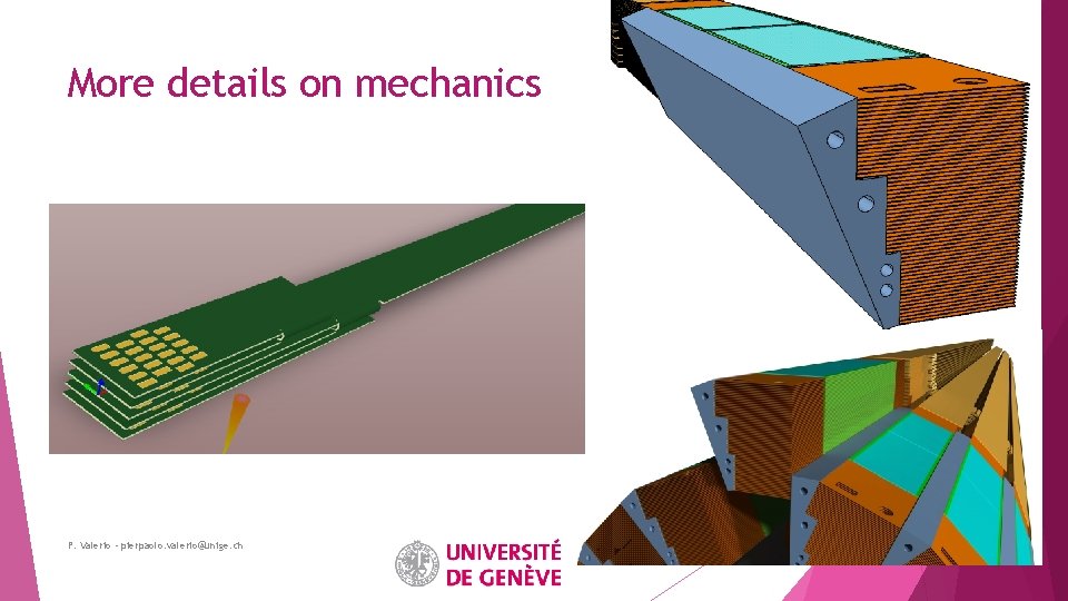
Scanner Architecture 16 wedge-shaped units, called “cells” A cell is a stack of ~70 detection layers Cell efficiency for 511 ke. V photons: up to 50%. More than 600. 000 channels on 2112 chips FEA simulations performed Cooling Block is currently under revisions for production and tests Flex design finalized, first prototype in production soon. P. Valerio - pierpaolo. valerio@unige. ch 13 -Sep-17 7 Courtesy of L. Paolozzi

Pros and cons of this approach Very high granularity, with access to depth and TOF information for every hit Faster signals mean ability to have high-precision timing measurements The scanner can be designed to be compatible with an MRI scanner, providing combined MRI-PET images On the other hand. . . The mechanics of the scanner are really complex (especially the data flex) There a very large number of channels, so the data acquisition scheme is critical Every channel must be calibrated very long procedure P. Valerio - pierpaolo. valerio@unige. ch 13 -Sep-17 8

Outline The TT-PET scanner Front-end architecture System integration Prototype measurements Next steps and conclusions P. Valerio - pierpaolo. valerio@unige. ch 13 -Sep-17 9

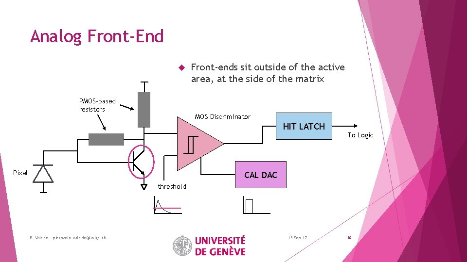
Analog Front-End PMOS-based resistors Front-ends sit outside of the active area, at the side of the matrix MOS Discriminator HIT LATCH Pixel To Logic CAL DAC threshold P. Valerio - pierpaolo. valerio@unige. ch 13 -Sep-17 10

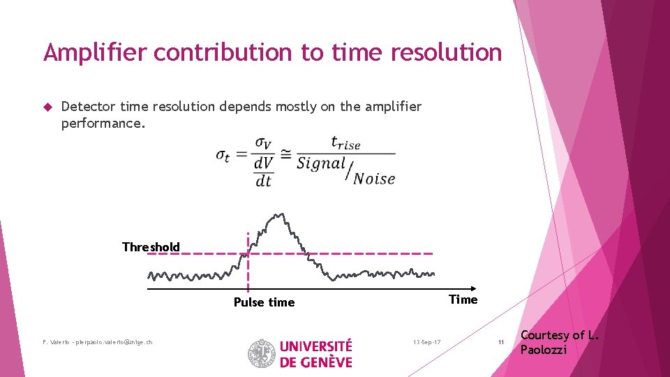
Amplifier contribution to time resolution Detector time resolution depends mostly on the amplifier performance. Threshold Time Pulse time P. Valerio - pierpaolo. valerio@unige. ch 13 -Sep-17 11 Courtesy of L. Paolozzi

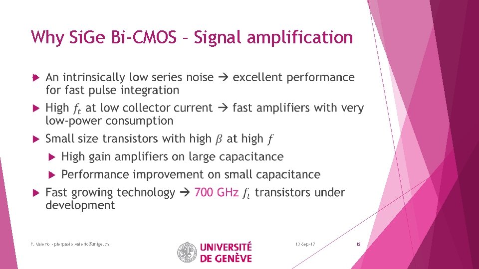
Why Si. Ge Bi-CMOS – Signal amplification P. Valerio - pierpaolo. valerio@unige. ch 13 -Sep-17 12

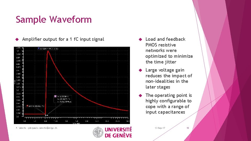
Sample Waveform Amplifier output for a 1 f. C input signal P. Valerio - pierpaolo. valerio@unige. ch Load and feedback PMOS resistive networks were optimized to minimize the time jitter Large voltage gain reduces the impact of non-idealities in the later stages The operating point is highly configurable to cope with a range of input capacitances 13 -Sep-17 13

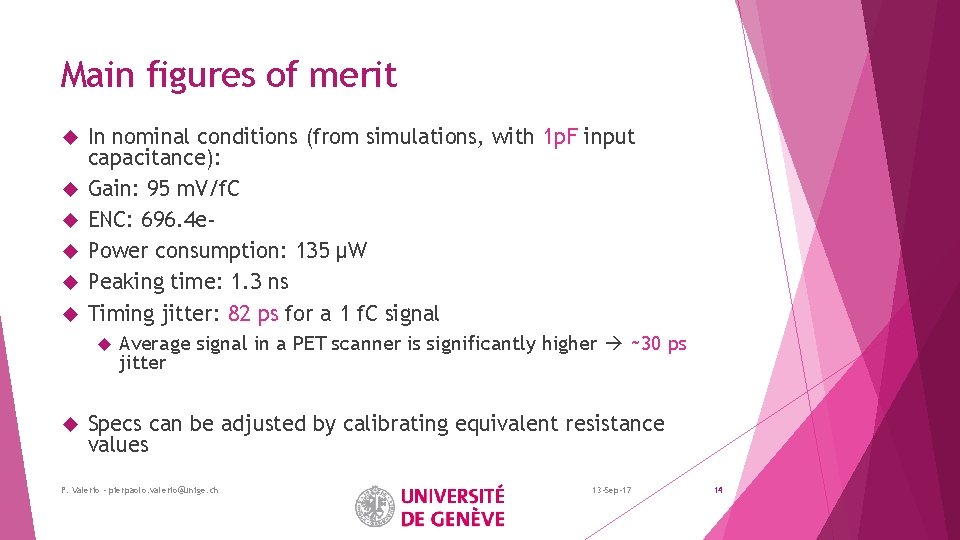
Main figures of merit In nominal conditions (from simulations, with 1 p. F input capacitance): Gain: 95 m. V/f. C ENC: 696. 4 e. Power consumption: 135 μW Peaking time: 1. 3 ns Timing jitter: 82 ps for a 1 f. C signal Average signal in a PET scanner is significantly higher ~30 ps jitter Specs can be adjusted by calibrating equivalent resistance values P. Valerio - pierpaolo. valerio@unige. ch 13 -Sep-17 14

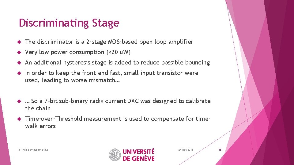
Discriminating Stage The discriminator is a 2 -stage MOS-based open loop amplifier Very low power consumption (<20 u. W) An additional hysteresis stage is added to reduce possible bouncing In order to keep the front-end fast, small input transistor were used, leading to worse mismatch… … So a 7 -bit sub-binary radix current DAC was designed to calibrate the chain Time-over-Threshold measurement is used to compensate for timewalk errors TT-PET general meeting 24 Nov 2016 15

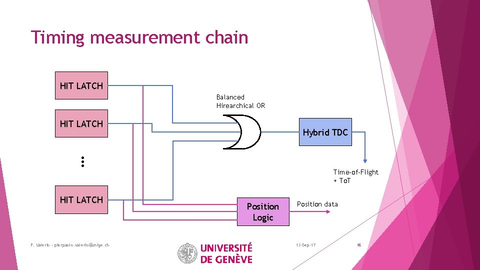
Timing measurement chain HIT LATCH Balanced Hirearchical OR HIT LATCH Hybrid TDC … Time-of-Flight + To. T HIT LATCH P. Valerio - pierpaolo. valerio@unige. ch Position Logic Position data 13 -Sep-17 16

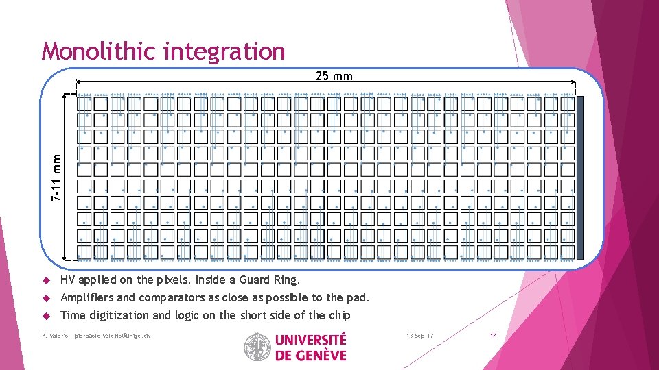
Monolithic integration 7 -11 mm 25 mm HV applied on the pixels, inside a Guard Ring. Amplifiers and comparators as close as possible to the pad. Time digitization and logic on the short side of the chip P. Valerio - pierpaolo. valerio@unige. ch 13 -Sep-17 17

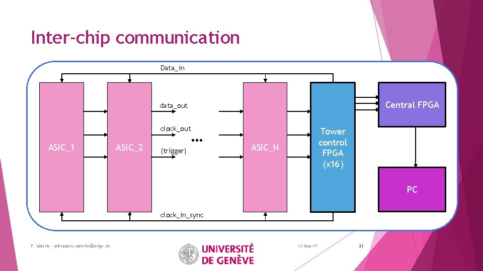
Chip readout Expected data rate is low enough that an on-chip 2 -stage buffering is enough to avoid pile-up The flex cable layout is critical and very challenging readout protocol with few lines chip daisy-chain Simple programming protocol to configure biasing and pixel calibration Serial readout at 50 Mbps with an optional triggering system P. Valerio - pierpaolo. valerio@unige. ch 13 -Sep-17 18

Outline The TT-PET scanner Front-end architecture System integration Prototype measurements Next steps and conclusions P. Valerio - pierpaolo. valerio@unige. ch 13 -Sep-17 19

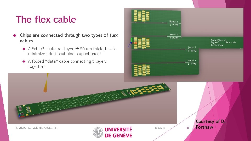
The flex cable Chips are connected through two types of flex cables A “chip” cable per layer 50 um thick, has to minimize additional pixel capacitance! A folded “data” cable connecting 5 layers together P. Valerio - pierpaolo. valerio@unige. ch 13 -Sep-17 20 Courtesy of D. Forshaw

Inter-chip communication Data_in Central FPGA data_out clock_out ASIC_1 ASIC_2 … (trigger) Tower control FPGA (x 16) ASIC_N PC clock_in_sync P. Valerio - pierpaolo. valerio@unige. ch 13 -Sep-17 21

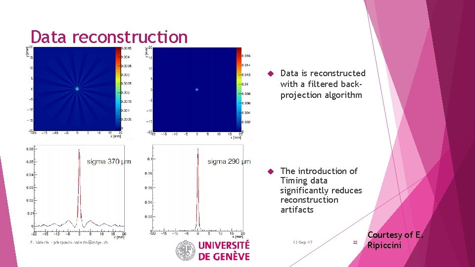
Data reconstruction P. Valerio - pierpaolo. valerio@unige. ch Data is reconstructed with a filtered backprojection algorithm The introduction of Timing data significantly reduces reconstruction artifacts 13 -Sep-17 22 Courtesy of E. Ripiccini

Outline The TT-PET scanner Front-end architecture System integration Prototype measurements Next steps and conclusions P. Valerio - pierpaolo. valerio@unige. ch 13 -Sep-17 23

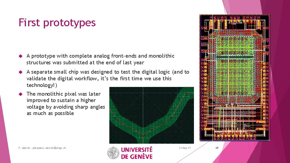
First prototypes A prototype with complete analog front-ends and monolithic structures was submitted at the end of last year A separate small chip was designed to test the digital logic (and to validate the digital workflow, it’s the first time we use this technology!) The monolithic pixel was later improved to sustain a higher voltage by avoiding sharp angles as much as possible P. Valerio - pierpaolo. valerio@unige. ch 13 -Sep-17 24

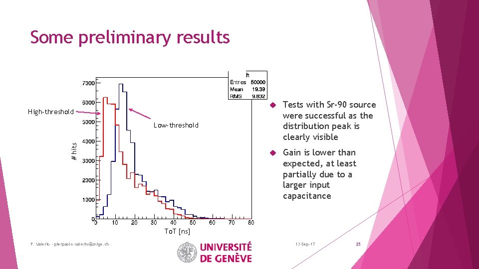
Some preliminary results High-threshold Tests with Sr-90 source were successful as the distribution peak is clearly visible Gain is lower than expected, at least partially due to a larger input capacitance # hits Low-threshold To. T [ns] P. Valerio - pierpaolo. valerio@unige. ch 13 -Sep-17 25

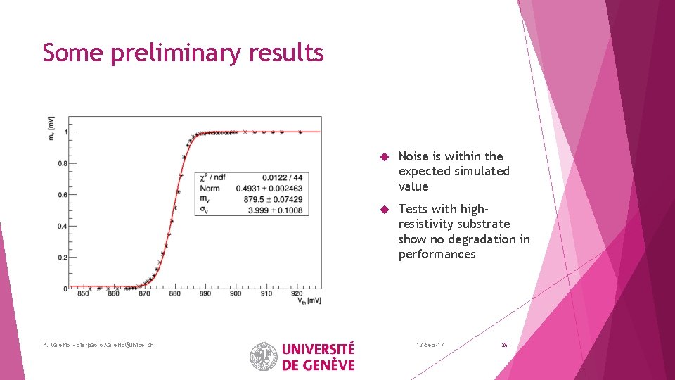
Some preliminary results P. Valerio - pierpaolo. valerio@unige. ch Noise is within the expected simulated value Tests with highresistivity substrate show no degradation in performances 13 -Sep-17 26

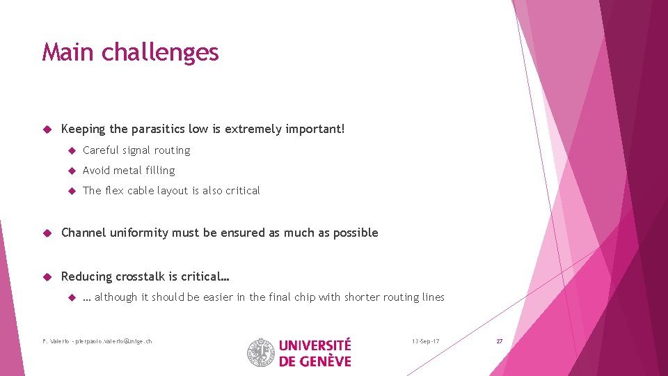
Main challenges Keeping the parasitics low is extremely important! Careful signal routing Avoid metal filling The flex cable layout is also critical Channel uniformity must be ensured as much as possible Reducing crosstalk is critical… … although it should be easier in the final chip with shorter routing lines P. Valerio - pierpaolo. valerio@unige. ch 13 -Sep-17 27

Other prototypes and ongoing tests A fully featured prototype was submitted in April It has a smaller matrix and a simplified readout scheme, but it's otherwise complete It's useful to test integration issues (power delivery, crosstalk. . . ) Tests are being set up as we speak P. Valerio - pierpaolo. valerio@unige. ch 13 -Sep-17 28

Outline The TT-PET scanner Front-end architecture System integration Prototype measurements Next steps and conclusions P. Valerio - pierpaolo. valerio@unige. ch 13 -Sep-17 29

Next submissions and design steps Some more test structures have been submitted to study the monolithic integration and improve isolation structures Smaller utility blocks are already designed and need to be integrated in the chip (bandgap, rail-to-rail buffers) After tests on the prototype, a final submission is tentatively scheduled for early next year P. Valerio - pierpaolo. valerio@unige. ch 13 -Sep-17 30

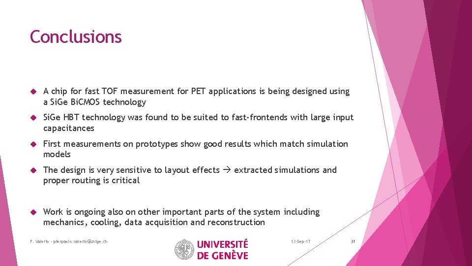
Conclusions A chip for fast TOF measurement for PET applications is being designed using a Si. Ge Bi. CMOS technology Si. Ge HBT technology was found to be suited to fast-frontends with large input capacitances First measurements on prototypes show good results which match simulation models The design is very sensitive to layout effects extracted simulations and proper routing is critical Work is ongoing also on other important parts of the system including mechanics, cooling, data acquisition and reconstruction P. Valerio - pierpaolo. valerio@unige. ch 13 -Sep-17 31

Thanks for your attention P. Valerio - pierpaolo. valerio@unige. ch 13 -Sep-17

BACKUP P. Valerio - pierpaolo. valerio@unige. ch 13 -Sep-17

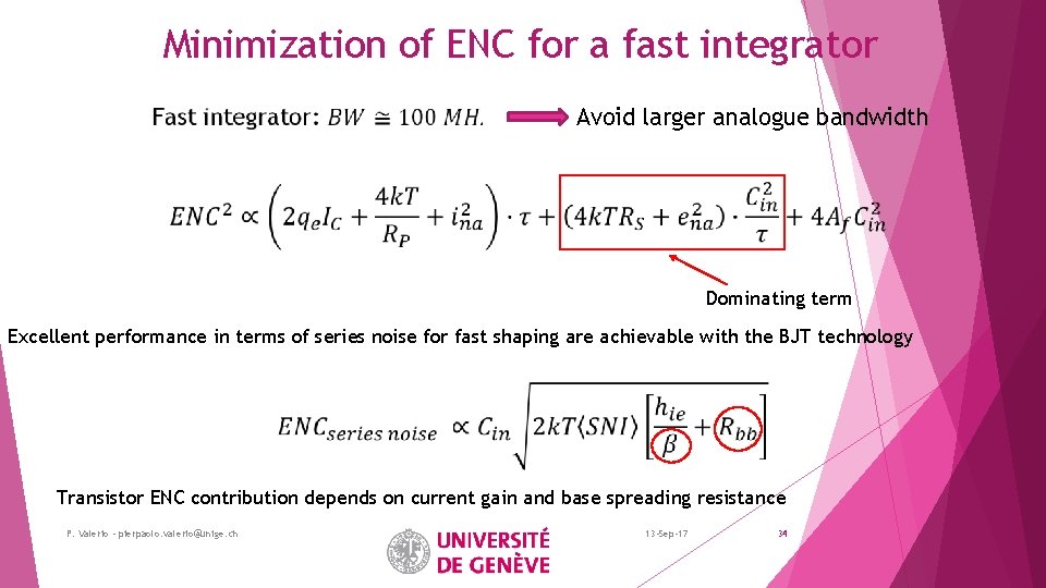
Minimization of ENC for a fast integrator Avoid larger analogue bandwidth Dominating term Excellent performance in terms of series noise for fast shaping are achievable with the BJT technology Transistor ENC contribution depends on current gain and base spreading resistance P. Valerio - pierpaolo. valerio@unige. ch 13 -Sep-17 34

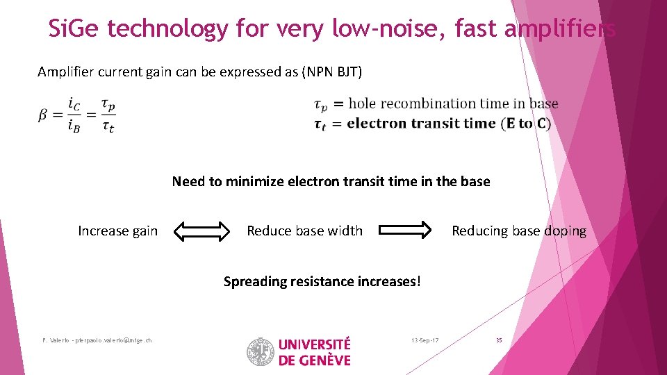
Si. Ge technology for very low-noise, fast amplifiers Amplifier current gain can be expressed as (NPN BJT) Need to minimize electron transit time in the base Increase gain Reduce base width Reducing base doping Spreading resistance increases! P. Valerio - pierpaolo. valerio@unige. ch 13 -Sep-17 35

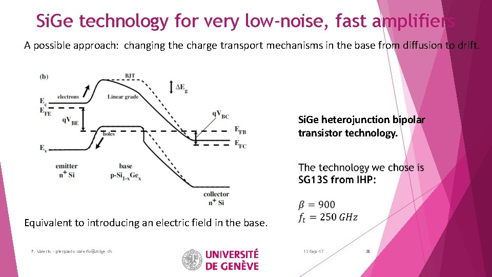
Si. Ge technology for very low-noise, fast amplifiers A possible approach: changing the charge transport mechanisms in the base from diffusion to drift. Si. Ge heterojunction bipolar transistor technology. Equivalent to introducing an electric field in the base. P. Valerio - pierpaolo. valerio@unige. ch 13 -Sep-17 36

More details on mechanics P. Valerio - pierpaolo. valerio@unige. ch 13 -Sep-17 37

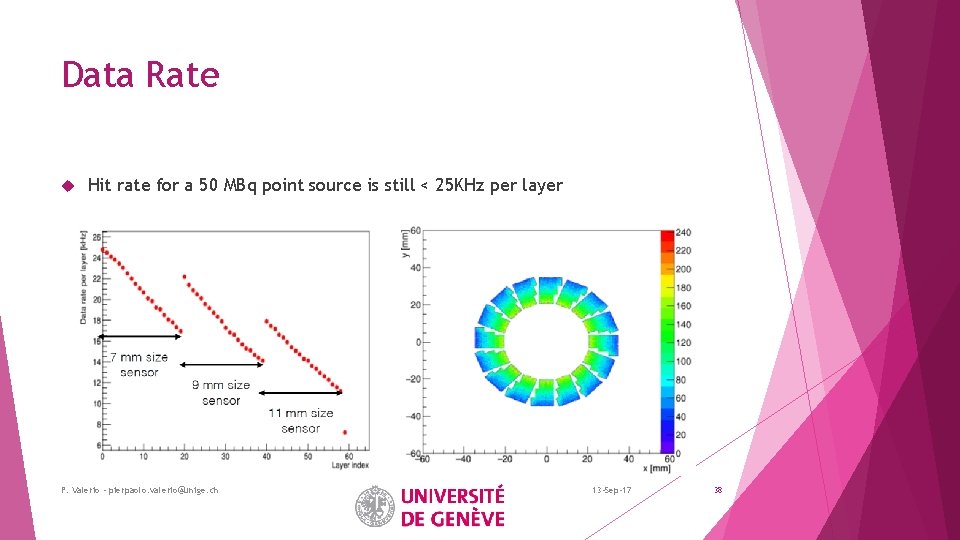
Data Rate Hit rate for a 50 MBq point source is still < 25 KHz per layer P. Valerio - pierpaolo. valerio@unige. ch 13 -Sep-17 38