A DataDriven Statistical Approach to Analyzing Process Variation
- Slides: 21

A Data-Driven Statistical Approach to Analyzing Process Variation in 65 nm SOI Technology ISQED 2007, San Jose, Mar 28, 2007 Choongyeun Cho 1, Daeik Kim 1, Jonghae Kim 1, Jean-Olivier Plouchart 1, Daihyun Lim 2, Sangyeun Cho 3, and Robert Trzcinski 1 Cho et al. 1 IBM, 2 MIT, 3 U. of Pittsburgh ISQED 2007

Outline § Introduction: § Motivation of this work § Constrained Principal Component Analysis § Proposed method § Experiments: § Using 65 nm SOI technology § Conclusion § Applications, future work § Contributions Cho et al. ISQED 2007 2

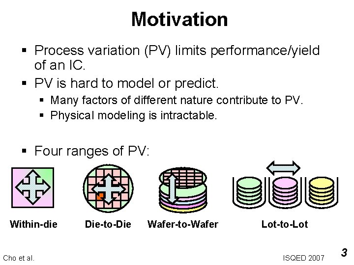
Motivation § Process variation (PV) limits performance/yield of an IC. § PV is hard to model or predict. § Many factors of different nature contribute to PV. § Physical modeling is intractable. § Four ranges of PV: Within-die Cho et al. Die-to-Die Wafer-to-Wafer Lot-to-Lot ISQED 2007 3

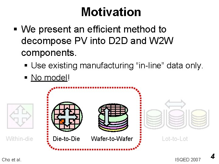
Motivation § We present an efficient method to decompose PV into D 2 D and W 2 W components. § Use existing manufacturing “in-line” data only. § No model! Within-die Cho et al. Die-to-Die Wafer-to-Wafer Lot-to-Lot ISQED 2007 4

What is In-line Data? § In this work, “in-line” data refers to: § Electrical measurements in manufacturing line using a parametric tester for various purposes: fault diagnosis, device dc characterization, and model-hardware correlation (MHC). § Thus, available very early in the manufacturing process. § Key PV parameters (VT, LPOLY, TOX, etc) are mostly embedded in in-line data yet in an obscure manner. § We statistically exploit in-line data to extract D 2 D and W 2 W variations individually. Cho et al. ISQED 2007 5

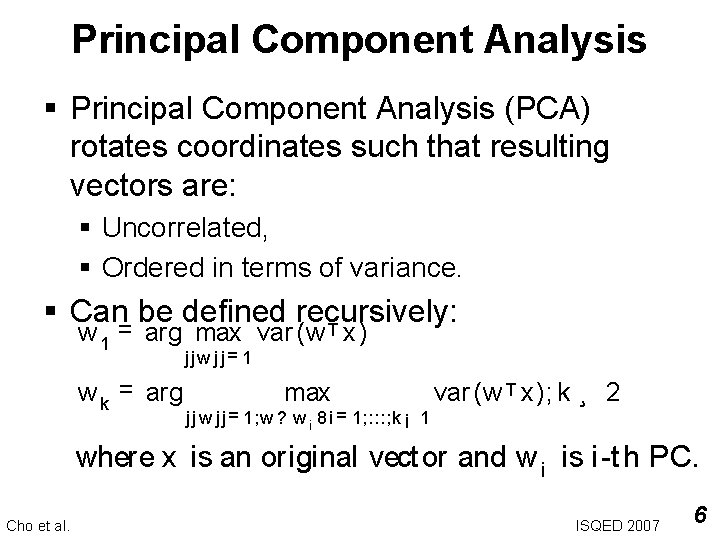
Principal Component Analysis § Principal Component Analysis (PCA) rotates coordinates such that resulting vectors are: § Uncorrelated, § Ordered in terms of variance. § Can= be defined recursively: T w 1 arg max var (w x) w k = arg jjw jj= 1 max j j w j j = 1; w ? w i 8 i = 1; : : : ; k ¡ 1 var (w T x); k ¸ 2 where x is an original vect or and w i is i -t h PC. Cho et al. ISQED 2007 6

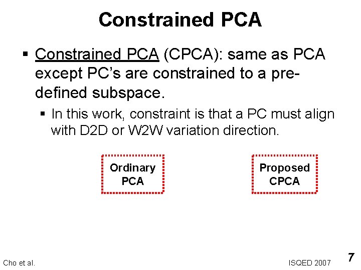
Constrained PCA § Constrained PCA (CPCA): same as PCA except PC’s are constrained to a predefined subspace. § In this work, constraint is that a PC must align with D 2 D or W 2 W variation direction. Ordinary PCA Cho et al. Proposed CPCA ISQED 2007 7

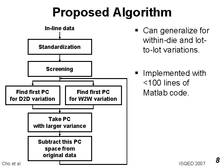
Proposed Algorithm In-line data Standardization Screening Find first PC for D 2 D variation Find first PC for W 2 W variation § Can generalize for within-die and lotto-lot variations. § Implemented with <100 lines of Matlab code. Take PC with larger variance Subtract this PC space from original data Cho et al. ISQED 2007 8

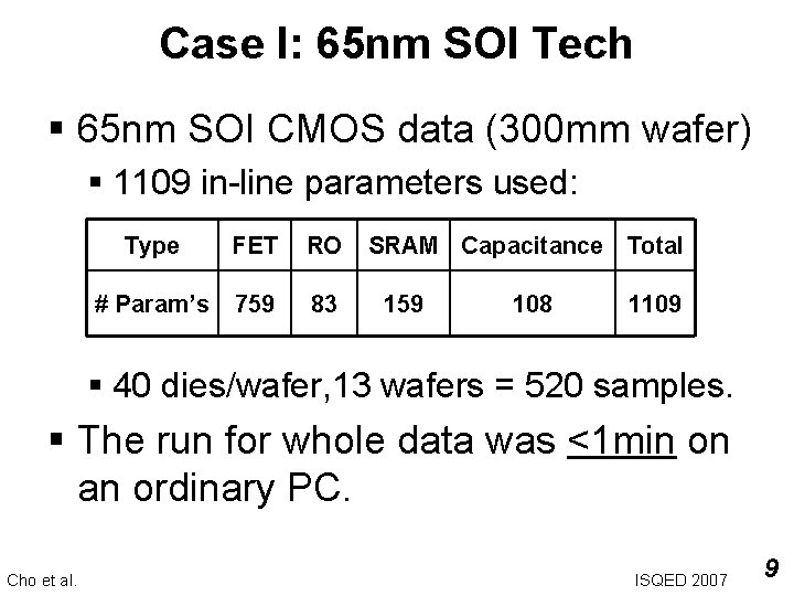
Case I: 65 nm SOI Tech § 65 nm SOI CMOS data (300 mm wafer) § 1109 in-line parameters used: Type FET RO # Param’s 759 83 SRAM Capacitance Total 159 108 1109 § 40 dies/wafer, 13 wafers = 520 samples. § The run for whole data was <1 min on an ordinary PC. Cho et al. ISQED 2007 9

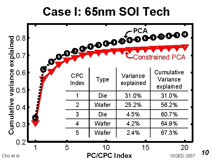
Cumulative variance explained Case I: 65 nm SOI Tech PCA 0. 8 0. 7 Constrained PCA 0. 6 Type Variance explained Cumulative Variance explained 1 Die 31. 0% 0. 4 2 Wafer 25. 2% 56. 2% 3 Die 4. 5% 60. 7% 0. 3 4 Wafer 4. 2% 64. 9% 5 Wafer 2. 4% 67. 3% 0. 5 0. 2 Cho et al. 1 5 CPC Index 10 PC/CPC Index 15 20 ISQED 2007 10

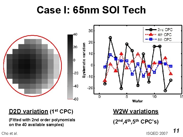
Case I: 65 nm SOI Tech D 2 D variation (1 st CPC) W 2 W variations (Fitted with 2 nd order polynomials on the 40 available samples) (2 nd, 4 th, 5 th CPC’s) Cho et al. ISQED 2007 11

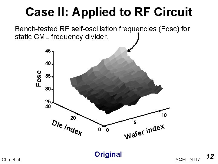
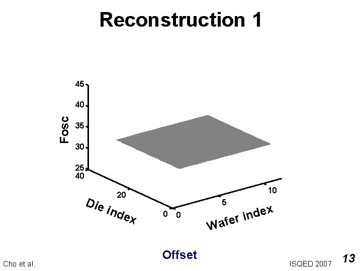
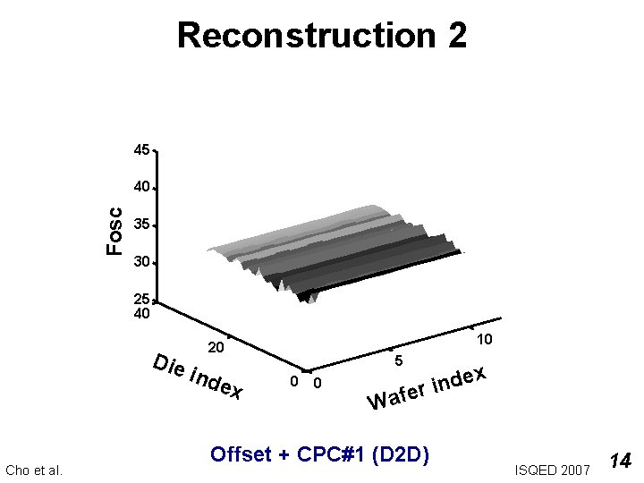
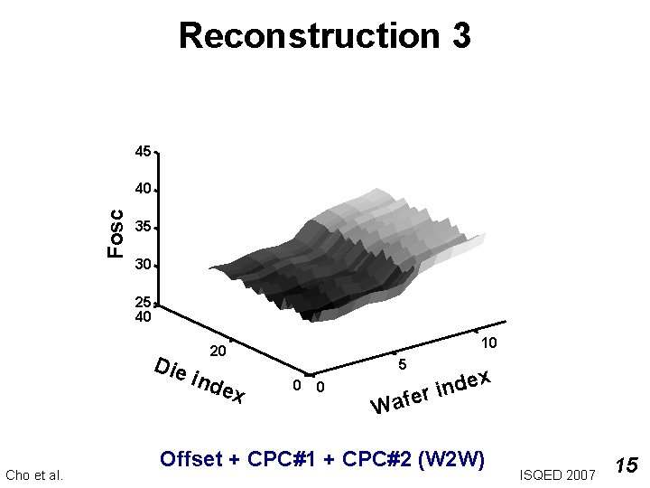
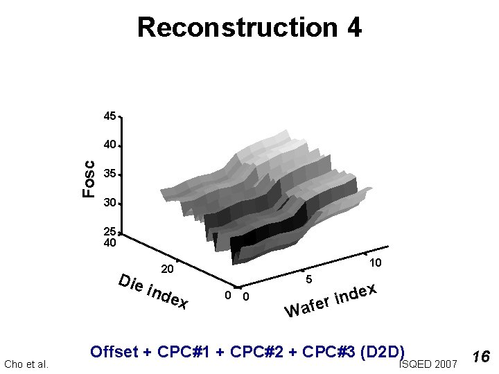
Case II: Applied to RF Circuit Bench-tested RF self-oscillation frequencies (Fosc) for static CML frequency divider. 45 Fosc 40 35 30 25 40 Die Cho et al. 10 20 ind Site ex 5 0 0 Original e d n i Wafer er f a W x ISQED 2007 12

Reconstruction 1 45 Fosc 40 35 30 25 40 Die Cho et al. 10 20 ind Site ex 5 0 0 Offset e d n i Wafer er f a W x ISQED 2007 13

Reconstruction 2 45 Fosc 40 35 30 25 40 Die Cho et al. 10 20 ind Site ex 5 0 0 e d n i Wafer er f a W Offset + CPC#1 (D 2 D) x ISQED 2007 14

Reconstruction 3 45 Fosc 40 35 30 25 40 Die Cho et al. 10 20 ind Site ex 5 0 0 e d n i Wafer er f a W x Offset + CPC#1 + CPC#2 (W 2 W) ISQED 2007 15

Reconstruction 4 45 Fosc 40 35 30 25 40 Die Cho et al. 10 20 ind Site ex 5 0 0 e d n i Wafer er f a W x Offset + CPC#1 + CPC#2 + CPC#3 (D 2 D) ISQED 2007 16

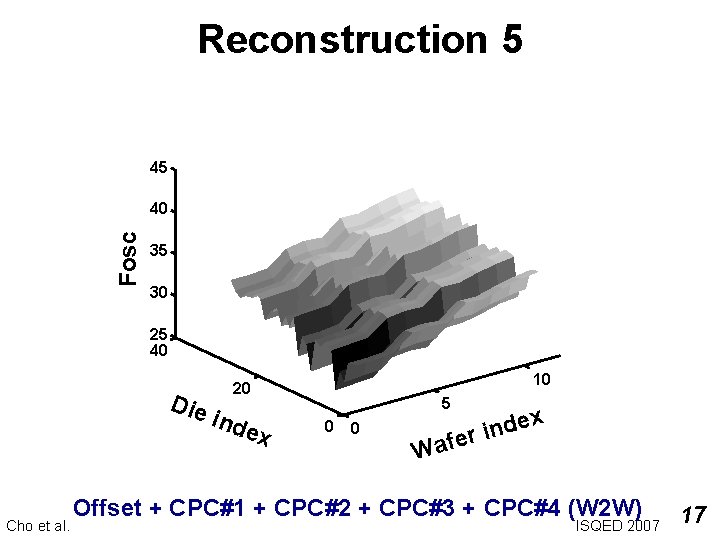
Reconstruction 5 45 Fosc 40 35 30 25 40 Die Cho et al. 10 20 ind Site ex 5 0 0 e d n i Wafer er f a W x Offset + CPC#1 + CPC#2 + CPC#3 + CPC#4 (W 2 W) ISQED 2007 17

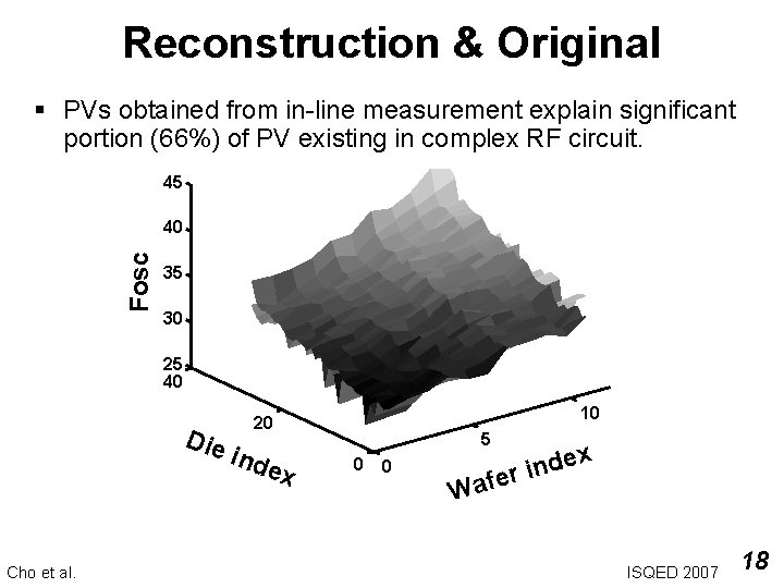
Reconstruction & Original § PVs obtained from in-line measurement explain significant portion (66%) of PV existing in complex RF circuit. 45 Fosc 40 35 30 25 40 Die Cho et al. 10 20 ind Site ex 5 0 0 e d n i Wafer er f a W x ISQED 2007 18

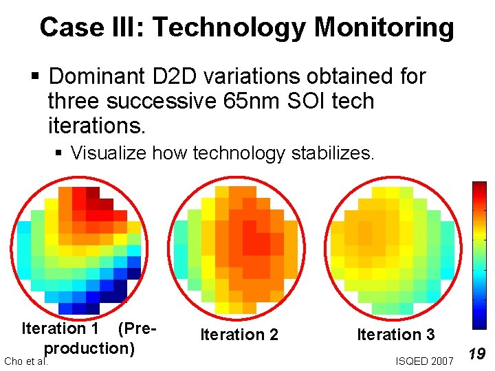
Case III: Technology Monitoring § Dominant D 2 D variations obtained for three successive 65 nm SOI tech iterations. § Visualize how technology stabilizes. Iteration 1 (Preproduction) Cho et al. Iteration 2 Iteration 3 ISQED 2007 19

Application / Future Work § Intelligent sampling: D 2 D variation signature may serve as a guideline to pick representative chips for sampled tests. § Technology snapshot: Use D 2 D variation to monitor characteristic of a given lot or technology. § Future work includes: § Incorporate within-die and lot-to-lot variations. § Statistical elaboration (Non-Gaussianity, etc). Cho et al. ISQED 2007 20

Contributions § Presented a statistical method to separate die-to-die and wafer-to-wafer variations using PCA variant: § Allows visualization and analysis of systematic variations. § Rapid feedback to tech development. § Verified that RF circuit performance is tied to device PV’s. Cho et al. ISQED 2007 21