A Common way of bandgap reference Widlar Bandgap

A Common way of bandgap reference

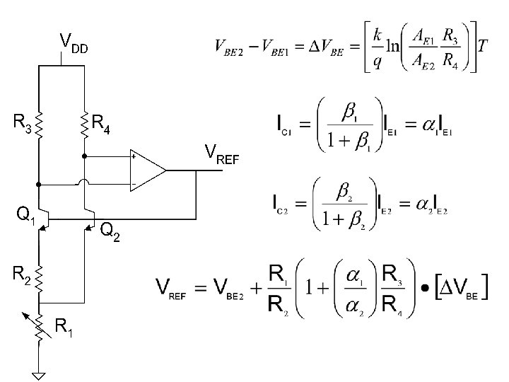
Widlar Bandgap Voltage Reference

Kuijk Bandgap Voltage Reference

Brokaw Bandgap Voltage Reference

Banba Bandgap Voltage Reference

Vref=I 3*R 3=

Converting bandgap voltage references to current references in general

Converting a bandgap voltage reference to a current reference Trim R 1 with intentional error in Vref, so that Vref temp co matches R 4 temp co.

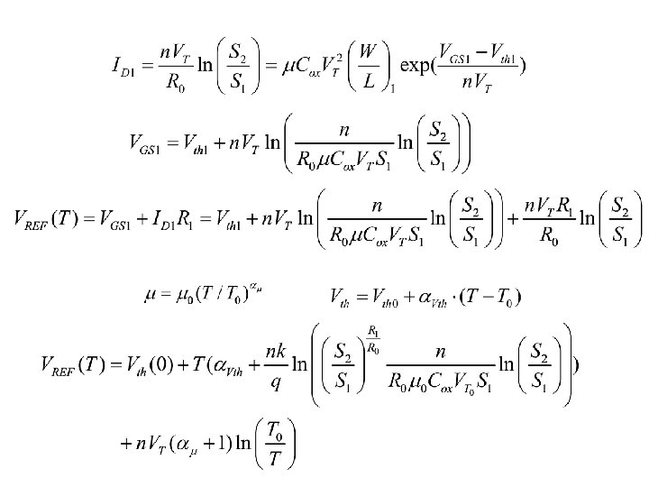
Kuijk circuit using CMOS in subthreshold

With a good op amp, ID 1=ID 2

Banba bandgap reference circuit Assuming an ideal op amp with an infinite gain, we have VA = VB and I 1 = I 2. Schematic of the current-mode bandgap circuit
=1. 17 V Since")
For the silicon, α=7. 021× 10 -4 V/K, β=1108 K, VG(0)=1. 17 V Since R 1=R 2, we know IC 1 = IC 2. Solving for Vbe 2: Substituting back

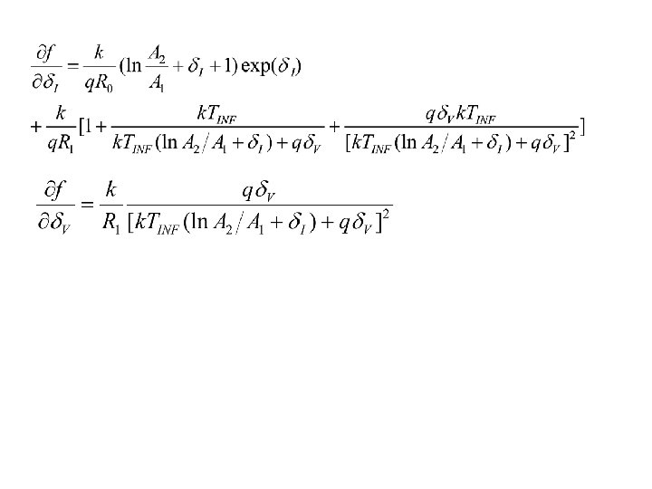
We know I 1=IC 1+VA/R 1. That gives Take partial derivative of I 1 with respect to temperature For a given temperature, set the above to 0 and solve for R 1. That tells you how to select R 1 in terms of temperature, area ratio, and R 0. Other quantities are device or process parameters.

In most literature, the last two items are ignored, that allows solution of inflection temperature T 0 in terms of R 0, R 1, area ratio: The current at the inflection point is

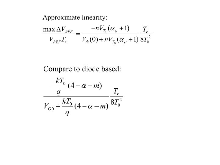
Curvature and sensitivity The second-order partial derivative of I 1 wrpt T is Notice that under a specific temperature, the second-order derivative is inversely proportional to the resistance R 1. We would like to have small variation of I 1 around TINF, so it is preferable to have a large R 1.

Denote the first derivative of I 1 by

The sensitivity of TINF wrpt R 0 and R 1 are For R 1 = 13. 74 KOhm and R 0 = 1 KOhm, the sensitivity wrpt R 0 is about -6. 75, and about 6. 5 wrpt R 1, when A 2/A 1 is equal to 8.

Effects of mismatch errors and the finite op amp gain First, suppose current mirror mismatch leads to mismatch between Ic 1 and Ic 2. In particular, suppose: Re-solve for VA

Finally we get the first line is IC 1 and the second is VA/R 1 The derivative of I 1 wrpt T becomes

Define similar to before: we can calculate

The sensitivity of TINF wrpt the current mismatch is This sensitivity is larger than those wrpt the resistances. That requires the current mismatch be controlled in an appropriate region so that the resistances can be used to effectively tune the temperature at the inflection point. The sensitivity of TINF wrpt the voltage difference is which means the inflection point temperature is not very sensitive to the voltage difference.

Bandgap circuit formed by transistors M 1, M 2, M 3, Q 1, Q 2, resistors R 0, R 2 A, R 2 B, and R 3. Cc is inter-stage compensation capacitor. Think of M 2 as the second stage of your two stage amplifier, then Cc is connected between output B and the input Vc.

• Amplifier: MA 1~MA 9, MA 9 is the tail current source, MA 1 and MA 2 consistent of the differential input pair of the op amp, MA 3~MA 6 form the current mirrors in the amplifier, MA 7 converts the amplifier output to single ended, and MA 5 and MA 8 form the push pull output node. – The offset voltage of the amplifier is critical factor, use large size differential input pair and careful layout; and use current mirror amplifier to reduce systematic offset. – 2 V supple voltage is sufficient to make sure that all the transistors in the amplifier work in saturation. – PMOS input differential pair is used because the input common mode range (A, B nodes) is changing approximately from 0. 8 to 0. 6 V and in this case NMOS input pair won’t work. • Self Bias: MA 10~MA 13, a self-bias approach is used in this circuit to bias the amplifier. Bias voltage for the primary stage current source MA 13 is provided by the output of the amplifier, i. e. there forms a selffeedback access from MA 8 drain output to bias current source MA 9 through current mirror MA 10~MA 13. • Startup Circuit: MS 1~MS 4. When the output of the amplifier is close to Vdd, the circuit will not work without the start-up circuit. With the start-up circuit MS 1 and MS 2 will conduct current into the BG circuit and the amplifier respectively.

Cc is 1 p. F To have better mirror accuracy, M 3 is driving a constant resistor Rtot. Capacitors at nodes A and B are added.

g. A is the total conductance of node A, and g. A = go 1+g. A’, g. B is the total conductance of node B, and g. B = go 2+g. B’, g. Z is the total conductance of node Z CA, CB and CZ are the total capacitance at nodes A, B and Z

Then the open loop transfer function from Vi+/- to Vo+/- is The transfer function with CC in place is

a nulling resistor RC can be added in series with CC to push z 1 to higher frequency

Loop gain simulation Cc=0 F , Phase Margin = 37. 86 o

Phase Margin = 47. 13 o Cc=1 p. F

Cc+R compensation, 1 p. F+20 k. Ohm Phase Margin = 74. 36 o


Curvature corrected bandgap circuit R 3 = R 4 Vref Q 2 Q 1 R 2 R 1

VBE T Vref T

Solution: R 4 = R 5 Vref IPTAT↓ D 2 D 1 R 2 R 3 IPTAT 2

Vref VBE VPTAT 2 T

HW: 1. Suppose you have an IPTAT 2 source characterized by IPTAT 2 = a. T 2, derive the conditions so that both first order and second order partial derivative of Vref with respect to T are canceled at a given temperature T 0. 2. Suggest a circuit schematic that can be used to generated IPTAT 2 current. You can use some of the circuit elements that we talked about earlier together with current mirrors/amplifiers to construct your circuit. Explain how your circuit work. If you found something in the literature, you can use/modify it but you should state so, give credit, and explain how the circuit works.

Characterization of a Current-Mode Bandgap Circuit Structure for High-Precision Reference Applications Hanqing Xing, Le Jin, Degang Chen and Randall Geiger Iowa State University 05/22/2006

Outline • Background on reference design • Introduction to our approach • Characterizing a multiple-segment reference circuit • Structure of reference system and curve transfer algorithm • Conclusion
 • References are widely used in electronic systems. • The")
Background on reference design(1) • References are widely used in electronic systems. • The thermal stability of the references plays a key role in the performance of many of these systems. • Basic idea behind commonly used “bandgap” voltage references is combining PTAT and CTAT sources to yield an approximately zero temperature coefficient (TC).
 • Linearly compensated bandgap references have a TC of about")
Background on reference design(2) • Linearly compensated bandgap references have a TC of about 20~50 ppm/o. C over 100 o. C. High order compensation can reduce TC to about 10~20 ppm /o. C over 100 o. C. • Unfortunately the best references available from industry no longer meet the performance requirements of emerging systems. System Resolution 12 bits 14 bits 16 bits TC requirement on reference 2. 44 ppm/o. C 0. 61 ppm/o. C 0. 15 ppm/o. C
 • “Envirostabilized references” – The actual operating environment of the")
Introduction to our approach(1) • “Envirostabilized references” – The actual operating environment of the device is used to stabilize the reference subject to temperature change. • Multiple-segment references – The basic bandgap circuit with linear compensation has a small TC near its inflection point but quite large TC at temperatures far from the inflection point. – High resolution can be achieved only if the device always operates near the inflection point. – Multiple reference segments with well distributed inflection points are used.
 A three-segment voltage reference # Curves 3 4 6 9")
Introduction to our approach(2) A three-segment voltage reference # Curves 3 4 6 9 TC (ppm/°C) 0. 8 0. 4 0. 2 0. 1 Accuracy (Bits) 13 14 15 16 Temperature range: -25°C~125°C
 Well known relationship between emitter current and VBE:")
Characterization of a bandgap circuit (1) Well known relationship between emitter current and VBE: For the silicon the values of the constants in (5) are, α=7. 021× 10 -4 V/K, β=1108 K and VG(0)=1. 17 V [2]. Schematic of the current-mode bandgap circuit
 • The inflection point temperature – The temperature")
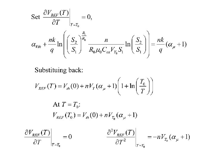
Characterization of a bandgap circuit (2) • The inflection point temperature – The temperature at the inflection point, TINF, will make the following partial derivative equal to zero. – It is difficult to get a closed form solution of TINF. Newton-Raphson method can be applied to find the local maxima of I 1 and the corresponding TINF associated with different circuit parameters.
 • The inflection point of Vref as a")
Characterization of a bandgap circuit (3) • The inflection point of Vref as a function of R 0
 • Output voltage at the inflection point •")
Characterization of a bandgap circuit (4) • Output voltage at the inflection point • With a fixed resistance ratio R 3/R 1, output voltage at the inflection point changes with the inflection point temperature. • Voltage level alignment is required.
 • The reference voltage changing with temperature")
Characterization of a bandgap circuit (5) • The reference voltage changing with temperature
 • Curvature of the linear compensated bandgap curve")
Characterization of a bandgap circuit (6) • Curvature of the linear compensated bandgap curve • There are only process parameters and temperature in the expression of the curvature. • The curvature can be well estimated although different circuit parameters are used.
 • 2 nd derivative of the bandgap curve")
Characterization of a bandgap circuit (7) • 2 nd derivative of the bandgap curve at different inflection point temperatures (emitter currents of Ckt 1 and Ckt 2 are 20 u. A and 50 u. A respectively and opamp gain is 80 d. B )
 • Three major factors that")
Structure of reference system and curve transfer algorithm (1) • Three major factors that make the design of a multi-segment voltage reference challenging – the precise positioning of the inflection points – the issue of aligning each segment with desired reference level and accuracy – establishing a method for stepping from one segment to another at precisely the right temperature in a continuous way
 • the precise positioning of")
Structure of reference system and curve transfer algorithm (2) • the precise positioning of the inflection points – The inflection point can be easily moved by adjusting R 0 – Equivalent to choosing a proper temperature range for each segment. – The same voltage level at two end points gives the correct reference curve. – With the information of the curvature, a proper choice of the temperature range makes sure the segment is within desired accuracy window.
 • aligning each segment with desired")
Structure of reference system and curve transfer algorithm(3) • aligning each segment with desired reference level and accuracy – The reference level can be easily adjusted by choosing different values of R 3, which will not affect the inflection point. – Comparison circuit with higher resolution is required to do the alignment.
 • Algorithm for stepping from one")
Structure of reference system and curve transfer algorithm(4) • Algorithm for stepping from one segment to another at precisely the right temperature in a continuous way – Determining the number of segments and the temperature range covered by each of them – Recording all the critical temperatures that are end points of the segments – Calibration done at those critical temperatures – Stepping algorithm
 • Stepping algorithm – When temperature")
Structure of reference system and curve transfer algorithm(5) • Stepping algorithm – When temperature rises to a critical temperature TC at first time, find correct R 0 and R 3 values for the segment used for next TR degrees – TR is the temperature range covered by the new segment
 • System diagram")
Structure of reference system and curve transfer algorithm(6) • System diagram

Conclusion • A new approach to design high resolution voltage reference • Explicit characterization of bandgap references • developed the system level architecture and algorithm
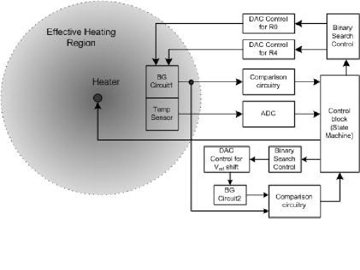

Heater: the dimension of the heater is quite small in comparison with that of the die. It is regarded as a point heat source. The shadow region is where the heater can effectively change the temperature of the die. BG Circuit and Temp Sensor are in the effective heating region. BG Circuit 1: the whole bandgap circuit includes bandgap structure, current mirror and the amplifier. R 0 and R 4 are both DAC controlled. BG Circuit 2: the backup BG reference circuit, the same structure as BG Circuit 1 but with only R 4 DAC controlled. Temp. Sensor: the temperature sensor, which can sense the temperature change instantaneously, is located close to the bandgap circuit and has the same distance to the heater as the bandgap circuit so that the temperature monitored represents the ambient temperature of the bandgap circuit. Need good temperature linearity. ADC: quantize analog outputs of the temperature sensor. Need 10 -bit linearity. Control Block: state machine is used as a controller, which receives the temperature sensing results and the comparison results and gives out control signals for binary search and heater. DAC Control for R 0 and R 4: provide the digital controls for R 0 and R 4 in bandgap structure. Binary Search: implement binary search for choosing right control signal for R 0 and R 4. Comparison Circuitry: compare the outputs of the bandgap outputs. It is capable of making a comparison differentially or single-ended between the bandgap outputs at two differential moments and two different temperatures. The comparison circuitry should be offset cancelled and have small enough comparison resolution (much higher than 16 -bit).

Curve transfer algorithm Prerequisites: • Calibrate the temperature sensor. The sensor needs to have good linearity. That means the outputs of the sensor is linear enough with the temperature. The ADC also needs good linearity for accurately indicating the temperature, 10 -bit linearity for 0. 1 degree C accuracy. • Get the basic characteristics of the bandgap curve, such as the temperature range covered by one curve under the desired accuracy requirement, and the number of curves needed. Assume the temperature range covered by one curve under 16 -bit accuracy is Tr, and with Tr degrees’ temperature change the output of the sensor changes Sr.

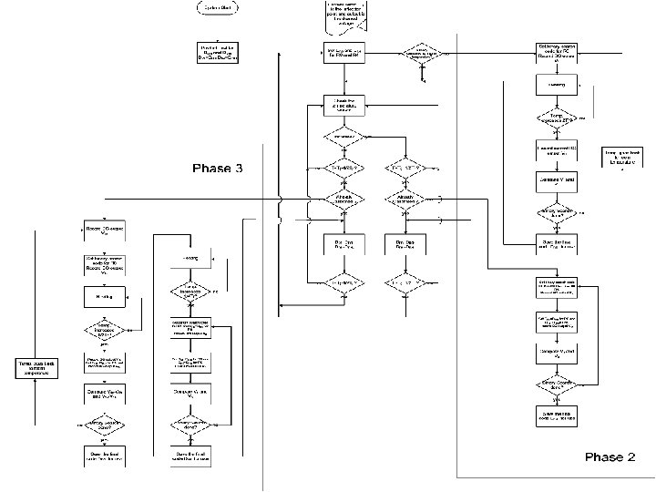
Procedure: • Phase 1: Production test, which gives correct DAC codes DR 00 and DR 40 for R 0’s and R 4’s controls to achieve a bandgap curve with its inflection point at current room temperature T 0 and its output voltage right now equal to the desired reference voltage V 0.

• Phase 2: At the temperature T 0, do the following to obtain R 0 and R 4 control codes of the next bandgap curve with higher inflection points DR 0 H and DR 4 H: – Step 1: Record the current output of the temperature sensor, as S 0, then reset the control code for R 0 (keep the code for R 4) to the first code in binary search, the output of the bandgap circuit is VL. – Step 2: Activate the heater and monitor the output of the sensor, stop the heater when the output arrives S 1=S 0+2 Sr (or a litter bit smaller), the current output of the bandgap circuit is VH with the R 0 code unchanged. – Step 3: Compare VL and VH with the comparison circuitry, continue the binary search for R 0 and set the new binary code according to the result of comparison. Wait until the output of the sensor back to S 0, then record the output code for the new code. – Step 4: Repeat the three steps above until the binary search for R 0 is done. The final code for R 0 can generate a new bandgap curve with its inflection at T 0+Tr. Store the new R 0 control code for future use, denoted as DR 0 H.

– Step 5: Monitor the ambient temperature change using the temperature sensor. When the output of the sensor rises to S 0+1/2 Sr, start comparing the two bandgap outputs with R 0 control code equal to DR 00 and DR 0 H respectively. Another binary search is applied to obtain the new R 4 control code DR 4 H, which ensure the two outputs in comparison are very close to each other. – Step 6: Monitor the output of the sensor, when it goes higher than S 0+1/2 Sr, the new codes for R 0 and R 4 are used and the curve transfer is finished. Keep monitoring the temperature change, when the output of the sensor goes to S 0+Sr (that means the current temperature is right at the inflection of the current curve), all the operations in the phase 2 can be repeated to get the next pare of codes for higher temperature.

• Phase 3: When the ambient temperature goes lower, heater algorithm does not work effectively. Another procedure is developed to transfer to the lower inflection point curves. Temperature lower than room temperature cannot be achieved intentionally. Therefore we can not predict control codes for the ideal next lower curve as what we do in higher temperature case. When the temperature goes to T 0 -1/2 Tr, in order to maintain the accuracy requirement we have to find another bandgap curve with inflection point lower than T 0, the best we can achieve is the curve with its inflection point right at T 0 -1/2 Tr. Thus for temperature range lower than initial room temperature T 0, we need curves with doubled density of curves in the higher temperature range. – Step 1: At the initial time with room temperature T 0, record the bandgap output voltage V 0 a and the current control code for R 0 DR 00. Monitor the temperature, when it goes to S 0 -1/2 Sr, note the bandgap output V 0 b and then reset the control code for R 0 to the first code of binary search, DBS 0. Record the bandgap output V 1 a.

– Step 2: Start heating. When the output of the sensor is back to S 0 record the bandgap output V 1 b. – Step 3: Do differential comparison between V 0 a-V 0 b and V 1 a-V 1 b. – Step 4: Wait for the sensor output back to S 0 -1/2 Sr, change the R 0 control code according to the comparison result. Record the bandgap output as V 3 a. – Step 5: Repeat step 2 to 4 until the binary search is done. The final control code for R 0 DR 0 L ensures the difference between V 0 a-V 0 b and V 1 a. V 1 b is very small and the inflection of the new bandgap curve is close to T 0 -1/2 Tr. Set R 0 control code as DR 0 L. – Step 6: Activate the heater until the output of the sensor is S 0 -1/4 Sr and keep this temperature. Initial the binary search for R 4. Compare the bandgap outputs of two curves with R 0 control codes DR 00 and DR 0 L respectively. Set the R 4 control code according to comparison results. The final code DR 4 L is the new control code for R 4, which ensures the two voltage in comparison are nearly equal. – Step 7: Set DR 0 L and DR 4 L for R 0 and R 4 to finish the curve transfer. Keep monitoring the temperature change, when the output of the sensor goes to S 0 -Sr (that means a new curve transfer needs to start), all the operations in the phase 3 can be repeated to get the next pare of codes for higher temperature.

• Phase 4: Monitor the output of the temperature sensor. If a calibrated curve transfer is needed, set the new control codes for R 0 and R 4 according to the former calibration results. If a new calibration is needed, Phase 2 (temperature goes higher) or Phase 3 (temperature goes lower) is executed to obtain the new control codes.

Proposed Circuit

Multi-Segment Bandgap Circuit

Multi-Segment Bandgap Circuit • Observations – Tinf is a function of R 0 – Vinf can be determined by R 4

Self-Calibration of Bandgap Circuit • Partition whole temperature range into small segments • Identify C 0, C 1 and C 2 as functions of R 0 through measurements • Use R 0 to set appropriate Tinf for each segment • Change R 4 to set the value of Vinf • Performance guaranteed by calibration after fabrication and packaging

Simulation Setup • TSMC 0. 35 mm process • Cascoded current mirrors with W/L = 30 mm /0. 4 mm • Diode junction area – A 1 = 10 mm 2 – A 2 = 80 mm 2 • • R 1 = R 2 = 6 KW R 3 + R 4 = 6 KW 2. 5 V supply Op amp in Veriloga with 70 d. B DC gain

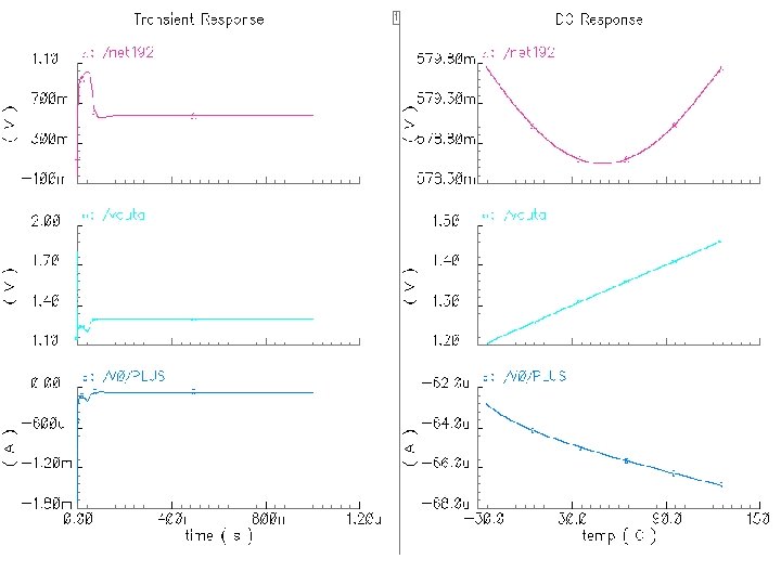
Tinf-R 0 Relationship • Vref measurement – R 0 ranging from 1150 to 1250 W with 1 W – T = 20, 22, and 24 C – Measured voltage has accuracy of 1 m. V • Top left: Actual and estimated Tinf as a function of R 0 • Bottom left: Error in estimation

Tinf-R 0 Relationship

Multi-Segment Bandgap Curve 60 -m. V variation over 140 C range gives 0. 36 ppm/ C
- Slides: 80