A CAD Tool for Scalable Floating Point Adder
A CAD Tool for Scalable Floating Point Adder Design and Generation Using C++/VHDL By Asim J. Al-Khalili AICCSA’ 06 Sharja 1
Overview • Introduction to Floating point Addition • Architecture of Single Path FADD • Activity Scaling • Triple Data Path Floating Point Adder • VHDL Modeling • Results • Implementation AICCSA’ 06 Sharja 2
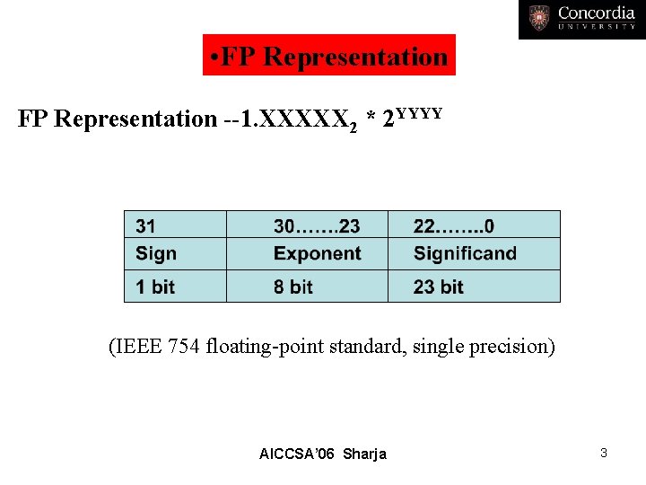
• FP Representation --1. XXXXX 2 * 2 YYYY (IEEE 754 floating-point standard, single precision) AICCSA’ 06 Sharja 3
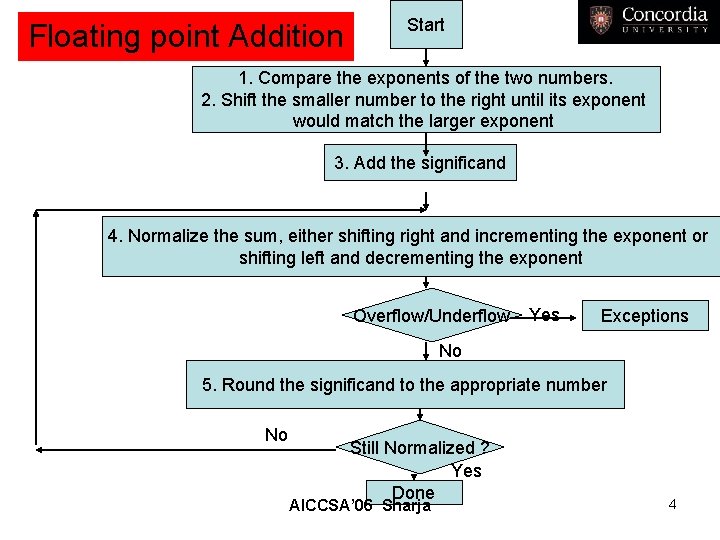
Floating point Addition Start 1. Compare the exponents of the two numbers. 2. Shift the smaller number to the right until its exponent would match the larger exponent 3. Add the significand 4. Normalize the sum, either shifting right and incrementing the exponent or shifting left and decrementing the exponent Overflow/Underflow Yes Exceptions No 5. Round the significand to the appropriate number No Still Normalized ? Yes Done AICCSA’ 06 Sharja 4
AICCSA’ 06 Sharja 5

What’s the best architecture? Architecture Consideration AICCSA’ 06 Sharja 6
• FP Adder Function include--- • Sign identification • Exponent comparison • Smaller significand right shift • Significand comparison ( If exp. are equal) • Significand inverter • Addition and Leading Zero anticipation • Normalization shifting left • Rounding • Shift after rounding • Compensation shifting • Exception handler AICCSA’ 06 Sharja 7
Architecture of TDPFADD AICCSA’ 06 Sharja 8
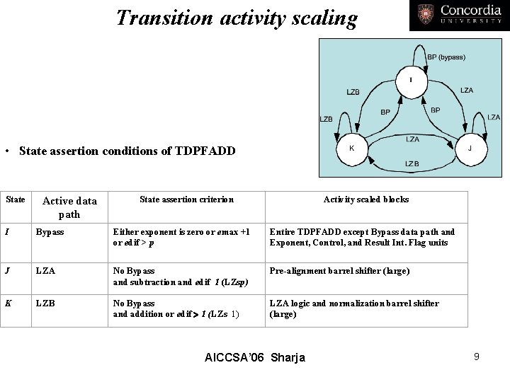
Transition activity scaling • State assertion conditions of TDPFADD State Active data path State assertion criterion Activity scaled blocks I Bypass Either exponent is zero or emax +1 Entire TDPFADD except Bypass data path and or edif > p Exponent, Control, and Result Int. Flag units J LZA No Bypass and subtraction and edif 1 (LZsp) Pre-alignment barrel shifter (large) K LZB No Bypass and addition or edif > 1 (LZs 1) LZA logic and normalization barrel shifter (large) AICCSA’ 06 Sharja 9
Probabilities of the Paths With IEEE single precision floating point data format, the probability that the FADD is in states A, B or C is given by P(A) = 0. 8177, P(B) = 0. 1765 and P(C) = 0. 0058. Here, it is assumed that the exponents are independent, uniformly distributed random variables and the events of addition and subtraction are equally likely. With IEEE double precision floating point format P(A) = 0. 9484, P(B) = 0. 0509 and P(C) = 7*10 -4. The time averaged power consumption (expected value) of a transition activity scaled FADD whose operational states are represented by Fig. 2 is given by Power=P(A)* PA + P(B) PB * + P(C ) * PC where PA, PB and PC represent the time averaged power consumption of the FADD in states A, B and C respectively. AICCSA’ 06 Sharja 10
Pipelined TDPFADD AICCSA’ 06 Sharja 11
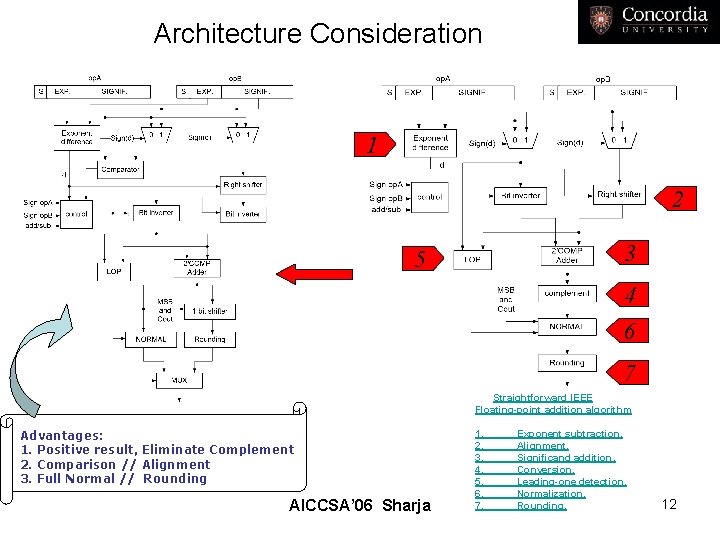
Architecture Consideration 1 2 3 5 4 6 7 Straightforward IEEE Floating-point addition algorithm Advantages: 1. Positive result, Eliminate Complement 2. Comparison // Alignment 3. Full Normal // Rounding AICCSA’ 06 Sharja 1. 2. 3. 4. 5. 6. 7. Exponent subtraction. Alignment. Significand addition. Conversion. Leading-one detection. Normalization. Rounding. 12
How can a compound adder compute fastest? Compound Adder AICCSA’ 06 Sharja 13
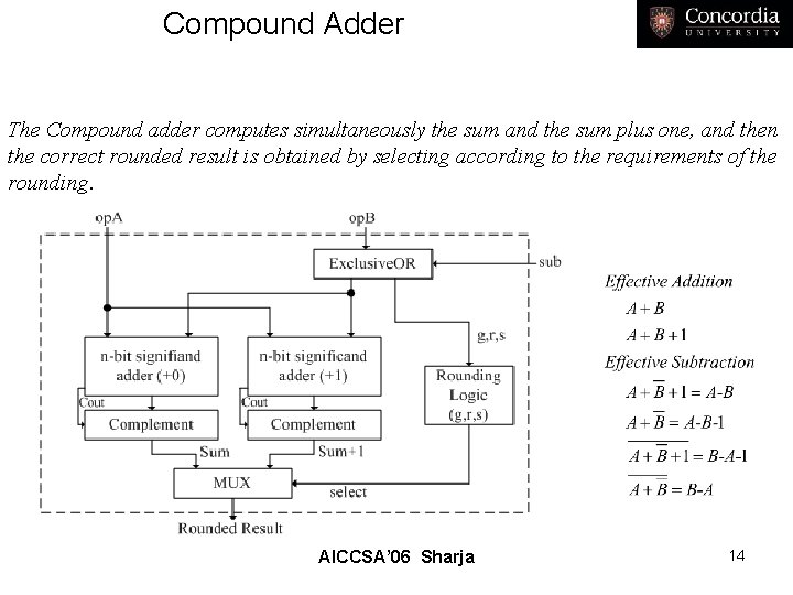
Compound Adder The Compound adder computes simultaneously the sum and the sum plus one, and then the correct rounded result is obtained by selecting according to the requirements of the rounding. AICCSA’ 06 Sharja 14
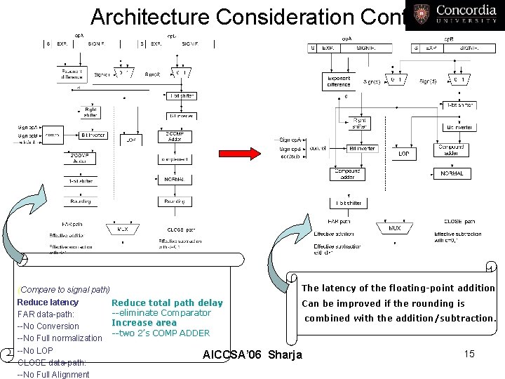
Architecture Consideration Cont. (Compare to signal path) Reduce latency Reduce total path delay --eliminate Comparator FAR data-path: Increase area --No Conversion --two 2’s COMP ADDER --No Full normalization --No LOP AICCSA’ 06 CLOSE data-path: --No Full Alignment The latency of the floating-point addition Can be improved if the rounding is combined with the addition/subtraction. Sharja 15

AICCSA’ 06 Sharja 16
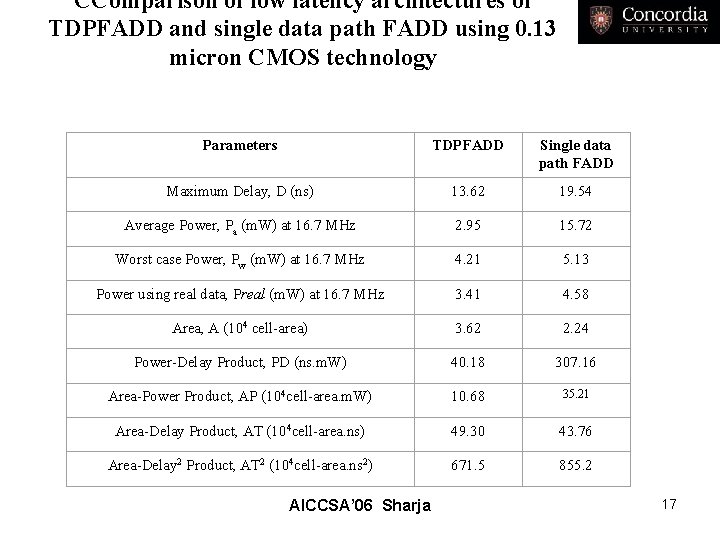
CComparison of low latency architectures of TDPFADD and single data path FADD using 0. 13 micron CMOS technology Parameters TDPFADD Single data path FADD Maximum Delay, D (ns) 13. 62 19. 54 Average Power, Pa (m. W) at 16. 7 MHz 2. 95 15. 72 Worst case Power, Pw (m. W) at 16. 7 MHz 4. 21 5. 13 Power using real data, Preal (m. W) at 16. 7 MHz 3. 41 4. 58 Area, A (104 cell-area) 3. 62 2. 24 Power-Delay Product, PD (ns. m. W) 40. 18 307. 16 Area-Power Product, AP (104 cell-area. m. W) 10. 68 35. 21 Area-Delay Product, AT (104 cell-area. ns) 49. 30 43. 76 Area-Delay 2 Product, AT 2 (104 cell-area. ns 2) 671. 5 855. 2 AICCSA’ 06 Sharja 17
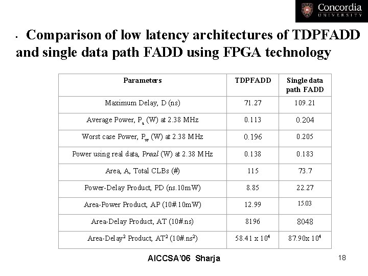
Comparison of low latency architectures of TDPFADD and single data path FADD using FPGA technology • Parameters TDPFADD Single data path FADD Maximum Delay, D (ns) 71. 27 109. 21 Average Power, Pa (W) at 2. 38 MHz 0. 113 0. 204 Worst case Power, Pw (W) at 2. 38 MHz 0. 196 0. 205 Power using real data, Preal (W) at 2. 38 MHz 0. 138 0. 183 Area, A, Total CLBs (#) 115 73. 7 Power-Delay Product, PD (ns. 10 m. W) 8. 85 22. 27 Area-Power Product, AP (10#. 10 m. W) 12. 99 15. 03 Area-Delay Product, AT (10#. ns) 8196 8048 Area-Delay 2 Product, AT 2 (10#. ns 2) 58. 41 x 104 87. 90 x 104 AICCSA’ 06 Sharja 18
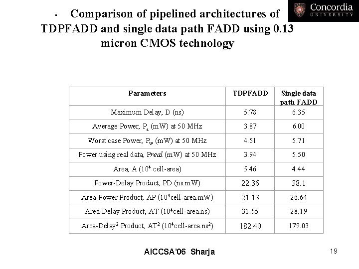
Comparison of pipelined architectures of • TDPFADD and single data path FADD using 0. 13 micron CMOS technology Parameters TDPFADD Maximum Delay, D (ns) 5. 78 Single data path FADD 6. 35 Average Power, Pa (m. W) at 50 MHz 3. 87 6. 00 Worst case Power, Pw (m. W) at 50 MHz 4. 51 5. 71 Power using real data, Preal (m. W) at 50 MHz 3. 94 5. 50 Area, A (104 cell-area) 5. 46 4. 44 Power-Delay Product, PD (ns. m. W) 22. 36 38. 1 Area-Power Product, AP (104 cell-area. m. W) 21. 13 26. 64 Area-Delay Product, AT (104 cell-area. ns) 31. 55 28. 19 Area-Delay 2 Product, AT 2 (104 cell-area. ns 2) 182. 40 179. 03 AICCSA’ 06 Sharja 19
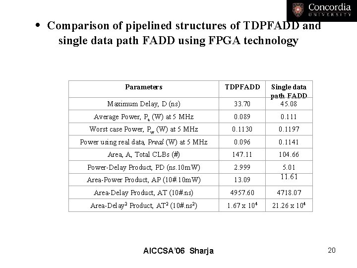
• Comparison of pipelined structures of TDPFADD and single data path FADD using FPGA technology Parameters TDPFADD Maximum Delay, D (ns) 33. 70 Single data path FADD 45. 08 Average Power, Pa (W) at 5 MHz 0. 089 0. 111 Worst case Power, Pw (W) at 5 MHz 0. 1130 0. 1197 Power using real data, Preal (W) at 5 MHz 0. 096 0. 1141 Area, A, Total CLBs (#) 147. 11 104. 66 Power-Delay Product, PD (ns. 10 m. W) 2. 999 5. 01 Area-Power Product, AP (10#. 10 m. W) 13. 09 11. 61 Area-Delay Product, AT (10#. ns) 4957. 60 4718. 07 Area-Delay 2 Product, AT 2 (10#. ns 2) 1. 67 x 104 21. 26 x 104 AICCSA’ 06 Sharja 20
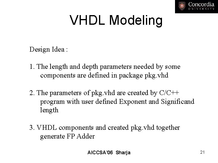
VHDL Modeling Design Idea : 1. The length and depth parameters needed by some components are defined in package pkg. vhd 2. The parameters of pkg. vhd are created by C/C++ program with user defined Exponent and Significand length 3. VHDL components and created pkg. vhd together generate FP Adder AICCSA’ 06 Sharja 21

VHDL Generation Get Parameter Length from user C++ program Calculate needed parameters Package Pkg. vhd Structural VHDL code of the floating point adder VHDL code Synthesize floating point adder hardware AICCSA’ 06 Sharja 22
Calculating the Parameters Using C/C++ AICCSA’ 06 Sharja 23
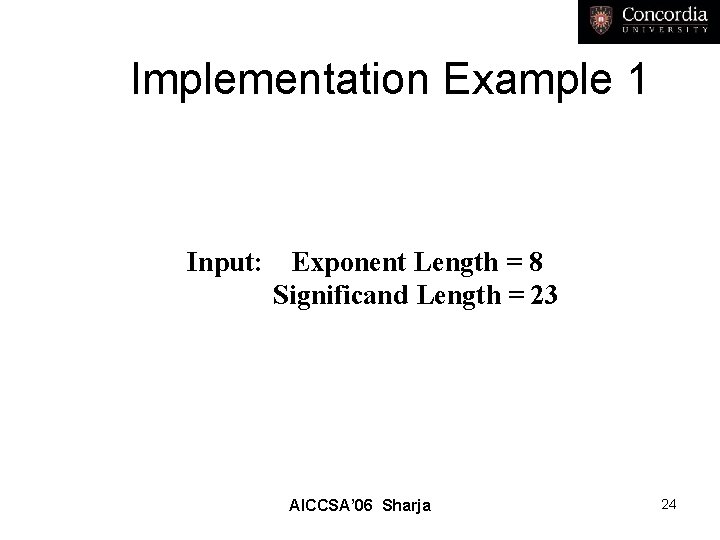
Implementation Example 1 Input: Exponent Length = 8 Significand Length = 23 AICCSA’ 06 Sharja 24
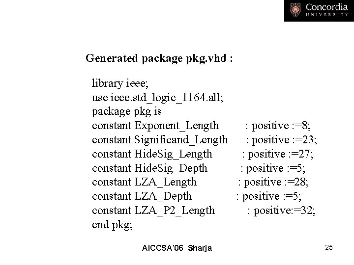
Generated package pkg. vhd : library ieee; use ieee. std_logic_1164. all; package pkg is constant Exponent_Length : positive : =8; constant Significand_Length : positive : =23; constant Hide. Sig_Length : positive : =27; constant Hide. Sig_Depth : positive : =5; constant LZA_Length : positive : =28; constant LZA_Depth : positive : =5; constant LZA_P 2_Length : positive: =32; end pkg; AICCSA’ 06 Sharja 25
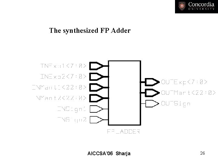
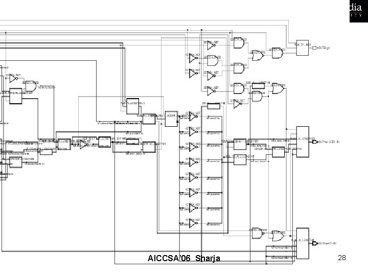
The synthesized FP Adder AICCSA’ 06 Sharja 26
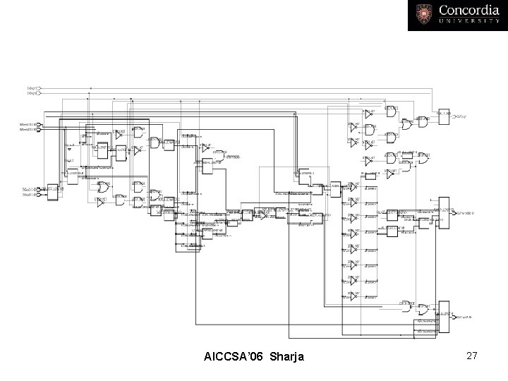
AICCSA’ 06 Sharja 27
AICCSA’ 06 Sharja 28
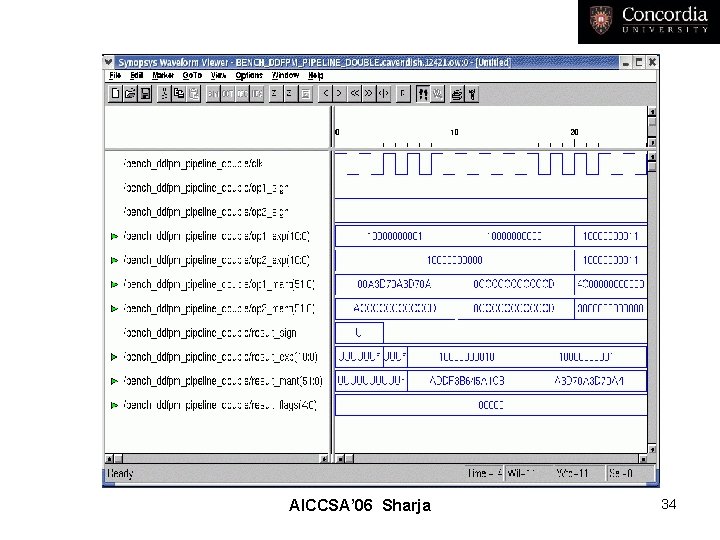
• Simulation and Test Result AICCSA’ 06 Sharja 29
Implementation Example 2 Input: Exponent Length = 4 Significand Length = 11 AICCSA’ 06 Sharja 30
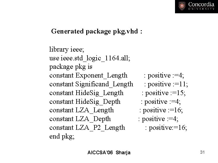
Generated package pkg. vhd : library ieee; use ieee. std_logic_1164. all; package pkg is constant Exponent_Length : positive : =4; constant Significand_Length : positive : =11; constant Hide. Sig_Length : positive : =15; constant Hide. Sig_Depth : positive : =4; constant LZA_Length : positive : =16; constant LZA_Depth : positive : =4; constant LZA_P 2_Length : positive: =16; end pkg; AICCSA’ 06 Sharja 31
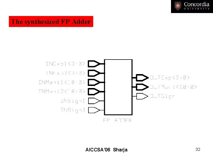
The synthesized FP Adder AICCSA’ 06 Sharja 32
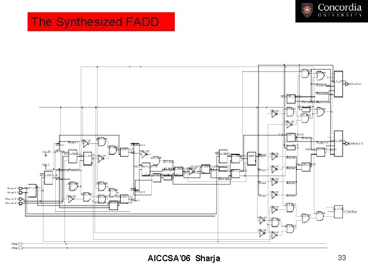
The Synthesized FADD AICCSA’ 06 Sharja 33
AICCSA’ 06 Sharja 34
Conclusion • A scalable-length FP adder is generated • The length of the adder is given by the user through C/C++ • The objective function is also stated • A structural mode FP adder is modeled by VHDL • The adder is Synthesizable • Depending on Power-Area-Delay requirement a Simple/TDPADD/Pipelined/PTDOADD is generated • The adder can also be pipelined AICCSA’ 06 Sharja 35

AICCSA’ 06 Sharja 36
• VHDL Modeling 1. Package for Length and Depth Parameters 2. Components of the FP Adder 3. Top Configuration of the FP Adder AICCSA’ 06 Sharja 37
1. Package for Length and Depth Parameters Input parameters : Significand length Exponent length Output parameters: significand length for calculation significand length for shifting significand depth for shifting Exponent length AICCSA’ 06 Sharja 38
• Exponent Difference Calculates the difference of the two exponents. AICCSA’ 06 Sharja 39
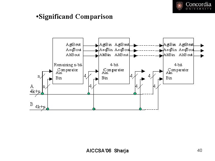
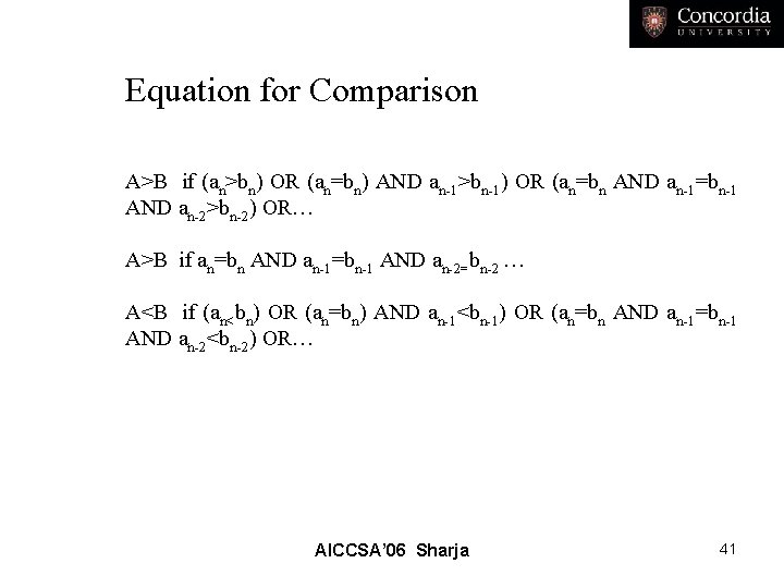
• Significand Comparison AICCSA’ 06 Sharja 40
Equation for Comparison A>B if (an>bn) OR (an=bn) AND an-1>bn-1) OR (an=bn AND an-1=bn-1 AND an-2>bn-2) OR… A>B if an=bn AND an-1=bn-1 AND an-2=bn-2 … A<B if (an<bn) OR (an=bn) AND an-1<bn-1) OR (an=bn AND an-1=bn-1 AND an-2<bn-2) OR… AICCSA’ 06 Sharja 41
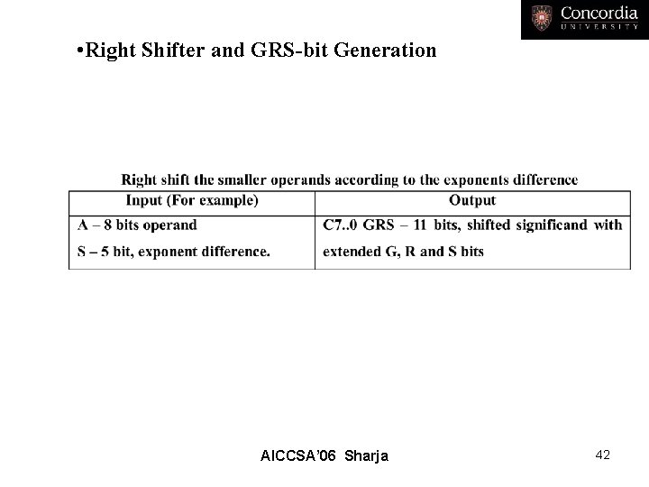
• Right Shifter and GRS-bit Generation AICCSA’ 06 Sharja 42
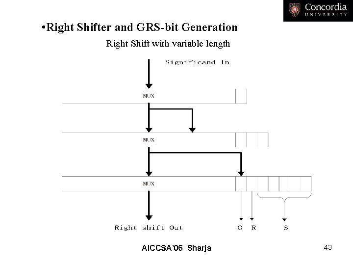
• Right Shifter and GRS-bit Generation Right Shift with variable length AICCSA’ 06 Sharja 43
• Manchester Adder/Subtractor AICCSA’ 06 Sharja 44

AICCSA’ 06 Sharja 45
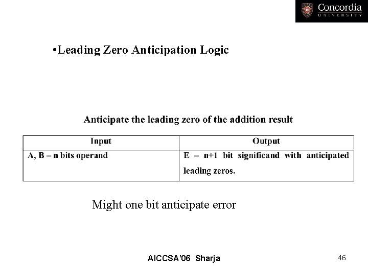
• Leading Zero Anticipation Logic Might one bit anticipate error AICCSA’ 06 Sharja 46
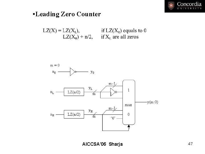
• Leading Zero Counter AICCSA’ 06 Sharja 47

• Normalization Shifter (left barrel shifter) AICCSA’ 06 Sharja 48
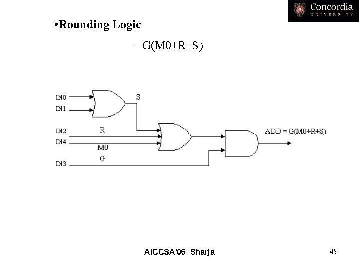
• Rounding Logic =G(M 0+R+S) AICCSA’ 06 Sharja 49
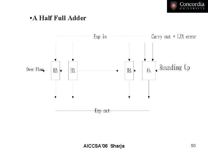
• A Half Full Adder AICCSA’ 06 Sharja 50
3. Top Configuration of FP Adder • Significand • Exponent • Sign • Exception Handling AICCSA’ 06 Sharja 51

• Significand AICCSA’ 06 Sharja 52

• Exponent AICCSA’ 06 Sharja 53
• Sign Select Logic 1. 2. Sign of larger exponent Exponent equal, sign of larger Significand AICCSA’ 06 Sharja 54
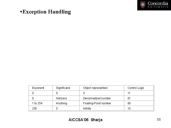
• Exception Handling Exponent Significand Object represented Control Logic 0 0 0 11 0 Nonzero Denormalized number 01 1 to 254 Anything Floating-Point number 00 255 0 Infinity 10 AICCSA’ 06 Sharja 55
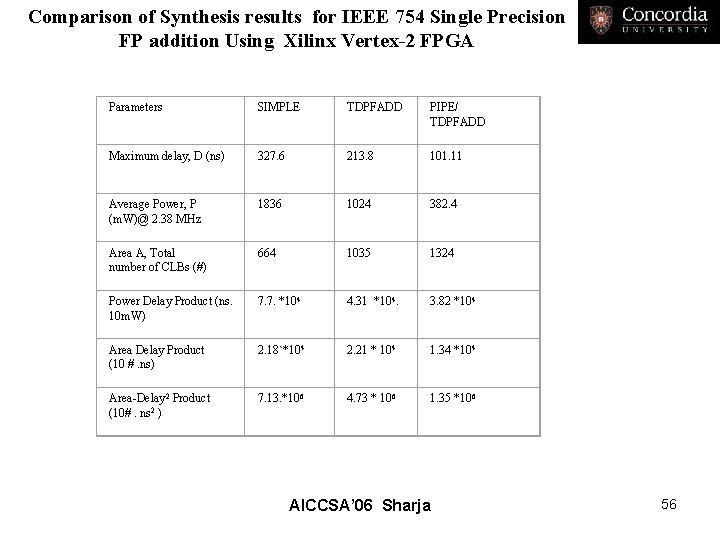
Comparison of Synthesis results for IEEE 754 Single Precision FP addition Using Xilinx Vertex-2 FPGA Parameters SIMPLE TDPFADD PIPE/ TDPFADD Maximum delay, D (ns) 327. 6 213. 8 101. 11 Average Power, P (m. W)@ 2. 38 MHz 1836 1024 382. 4 Area A, Total number of CLBs (#) 664 1035 1324 Power Delay Product (ns. 10 m. W) 7. 7. *104 4. 31 *104. 3. 82 *104 Area Delay Product (10 #. ns) 2. 18`*104 2. 21 * 104 1. 34 *104 Area-Delay 2 Product (10#. ns 2 ) 7. 13. *106 4. 73 * 106 1. 35 *106 AICCSA’ 06 Sharja 56
Main Blocks What blocks are considered? • Compound Adder with Flagged Prefix Adder (New) • LOP with Concurrent Position Correction (New) • Alignment Shifter • Normalization Shifter AICCSA’ 06 Sharja 57
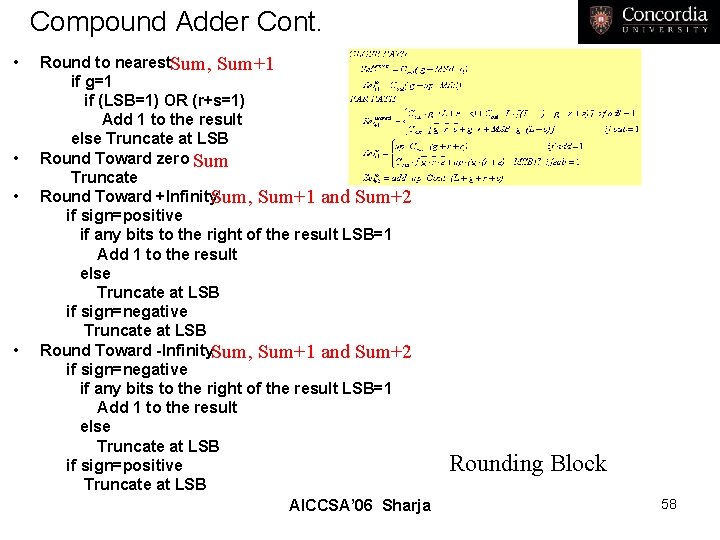
Compound Adder Cont. • • Round to nearest. Sum, Sum+1 if g=1 if (LSB=1) OR (r+s=1) Add 1 to the result else Truncate at LSB Round Toward zero Sum Truncate Round Toward +Infinity. Sum, Sum+1 and Sum+2 if sign=positive if any bits to the right of the result LSB=1 Add 1 to the result else Truncate at LSB if sign=negative Truncate at LSB Round Toward -Infinity. Sum, Sum+1 and Sum+2 if sign=negative if any bits to the right of the result LSB=1 Add 1 to the result else Truncate at LSB if sign=positive Truncate at LSB AICCSA’ 06 Sharja Rounding Block 58
- Slides: 58