A 128 channel eventdriven readout ASIC for the
- Slides: 31

A 128 -channel event-driven readout ASIC for the R 3 B Tracker TWEPP 2015, Lisbon Lawrence Jones ASIC Design Group Science and Technology Facilities Council Rutherford Appleton Laboratory

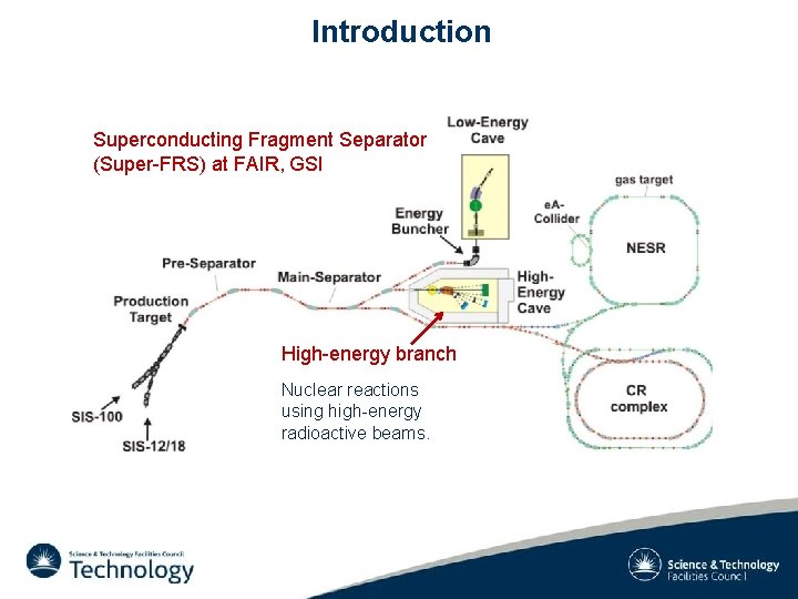
Introduction Superconducting Fragment Separator (Super-FRS) at FAIR, GSI High-energy branch Nuclear reactions using high-energy radioactive beams.

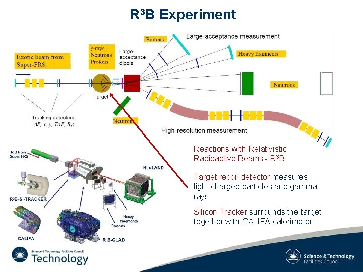
R 3 B Experiment Reactions with Relativistic Radioactive Beams - R 3 B Target recoil detector measures light charged particles and gamma rays Silicon Tracker surrounds the target together with CALIFA calorimeter

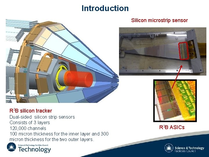
Introduction Silicon microstrip sensor R 3 B silicon tracker Dual-sided silicon strip sensors Consists of 3 layers 120, 000 channels 100 micron thickness for the inner layer and 300 micron thickness for the two outer layers. R 3 B ASICs

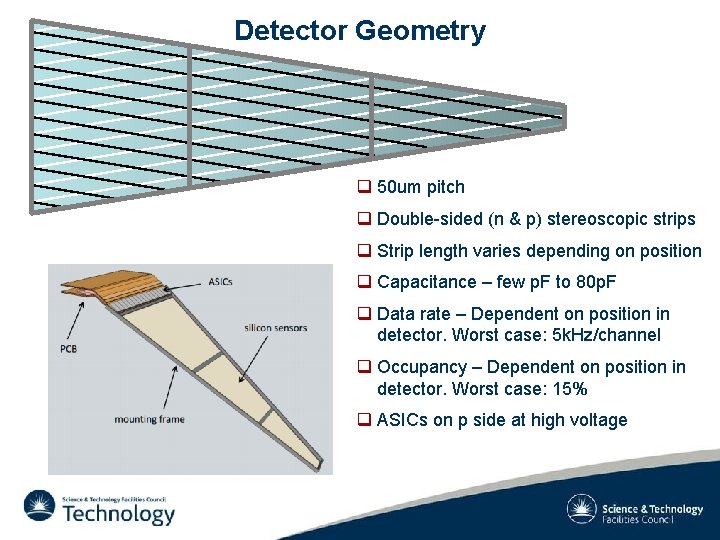
Detector Geometry q 50 um pitch q Double-sided (n & p) stereoscopic strips q Strip length varies depending on position q Capacitance – few p. F to 80 p. F q Data rate – Dependent on position in detector. Worst case: 5 k. Hz/channel q Occupancy – Dependent on position in detector. Worst case: 15% q ASICs on p side at high voltage

Challenges q Proton rate is ~100 s of Hz q Delta electron (background) rate ~100 s of k. Hz (some reactions) q Worst case count rate limited by ADC occupancy q Califa calorimeter will see the protons but not the electrons q Califa produces a “proton detected” validation signal to the ASIC q Tells ASIC to only buffer events when validation is high q The front end must cope with the 100 k. Hz electron rate even if the data is not read out q The front end must also recover from 1 Ge. V signals caused by beam misalignment q High dynamic range 50 Me. V (2 V), low threshold 100 ke. V (2 m. V) q Transistor mismatch

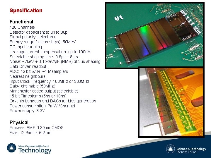
Specification Functional 128 Channels Detector capacitance: up to 80 p. F Signal polarity: selectable Energy range (silicon strips): 50 Me. V DC input coupling Leakage current compensation: up to 100 n. A Selectable shaping time: 0. 5 ms – 8 ms Noise: ~7 ke. V + 0. 15 ke. V/p. F (RMS) at 2 us shaping Data Driven readout ADC: 12 bit SAR, ~1 Msample/s Nearest neighbours Input Clock Frequency: 100 MHz or 200 MHz Daisy chainable (50 MHz) Manchester coded output (selectable) 15 bit Timestamp (5 ns or 10 ns) On-chip bandgap and DACs for bias generation Power consumption: 7 m. W /Channel Power supply: 3. 3 V Physical Process: AMS 0. 35 um CMOS Size: 12. 9 mm x 6. 2 mm

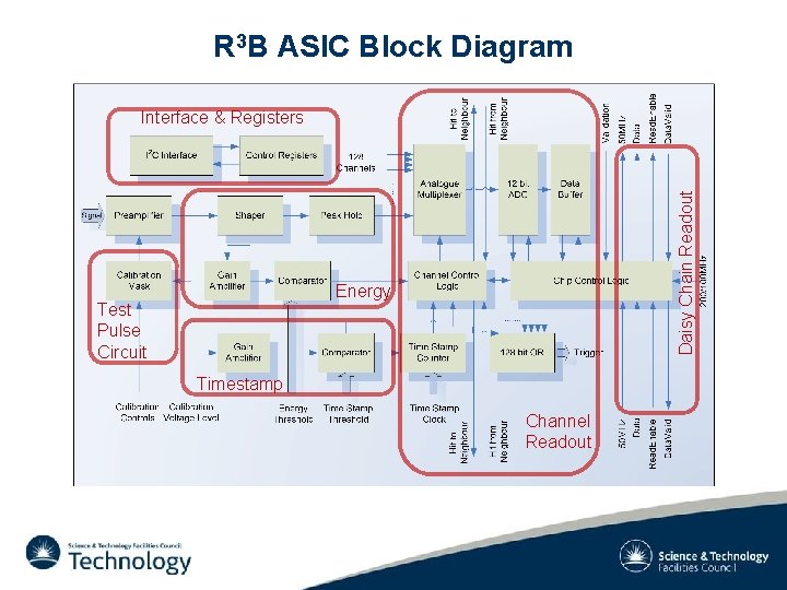
R 3 B ASIC Block Diagram Daisy Chain Readout Interface & Registers Energy Test Pulse Circuit Timestamp Channel Readout

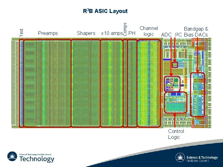
Preamps Shapers Comps Test R 3 B ASIC Layout x 10 amps Channel Bandgap & PH logic ADC I 2 C Bias DACs Control Logic

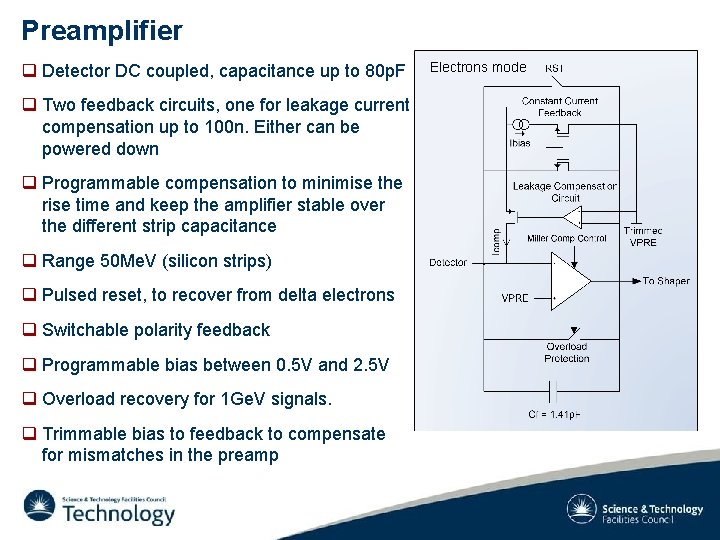
Preamplifier q Detector DC coupled, capacitance up to 80 p. F q Two feedback circuits, one for leakage current compensation up to 100 n. Either can be powered down q Programmable compensation to minimise the rise time and keep the amplifier stable over the different strip capacitance q Range 50 Me. V (silicon strips) q Pulsed reset, to recover from delta electrons q Switchable polarity feedback q Programmable bias between 0. 5 V and 2. 5 V q Overload recovery for 1 Ge. V signals. q Trimmable bias to feedback to compensate for mismatches in the preamp Electrons mode

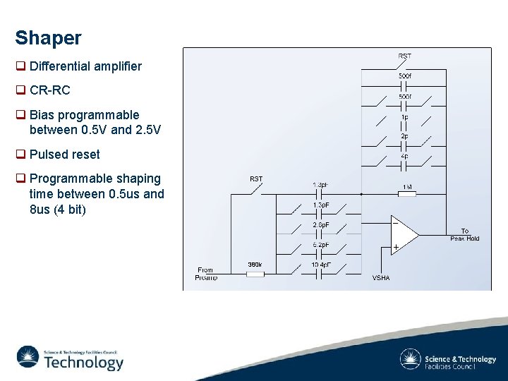
Shaper q Differential amplifier q CR-RC q Bias programmable between 0. 5 V and 2. 5 V q Pulsed reset q Programmable shaping time between 0. 5 us and 8 us (4 bit) 380 k

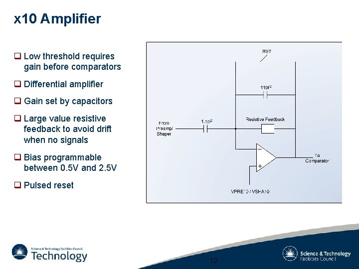
x 10 Amplifier q Low threshold requires gain before comparators q Differential amplifier q Gain set by capacitors q Large value resistive feedback to avoid drift when no signals q Bias programmable between 0. 5 V and 2. 5 V q Pulsed reset 12

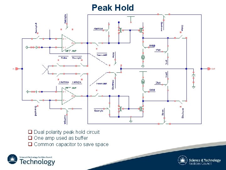
Peak Hold q Dual polarity peak hold circuit q One amp used as buffer q Common capacitor to save space

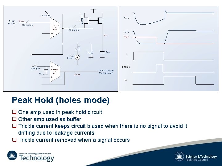
Peak Hold (holes mode) q One amp used in peak hold circuit q Other amp used as buffer q Trickle current keeps circuit biased when there is no signal to avoid it drifting due to leakage currents q Trickle current removed when a signal occurs

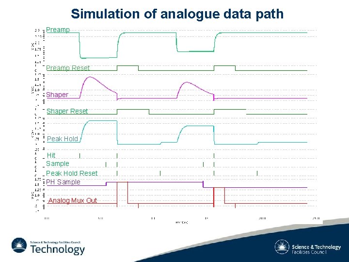
Simulation of analogue data path Preamp Reset Shaper Reset Peak Hold Hit Sample Peak Hold Reset PH Sample Analog Mux Out

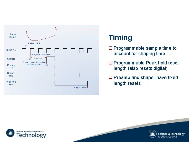
Timing q Programmable sample time to account for shaping time q Programmable Peak hold reset length (also resets digital) q Preamp and shaper have fixed length resets

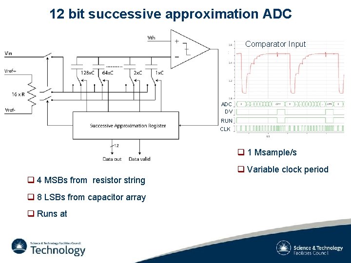
12 bit successive approximation ADC Comparator Input ADC DV RUN CLK q 1 Msample/s q Variable clock period q 4 MSBs from resistor string q 8 LSBs from capacitor array q Runs at

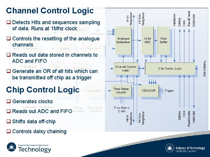
Channel Control Logic q Detects Hits and sequences sampling of data. Runs at 1 Mhz clock q Controls the resetting of the analogue channels q Reads out data stored in channels to ADC and FIFO q Generate an OR of all hits which can be transmitted off chip as a trigger Chip Control Logic q Generates clocks q Reads out ADC and FIFO q Shifts data off-chip q Controls daisy chaining

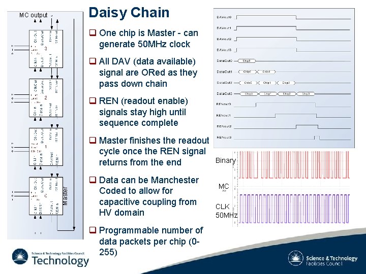
Daisy Chain MC output q One chip is Master - can generate 50 MHz clock q All DAV (data available) signal are ORed as they pass down chain q REN (readout enable) signals stay high until sequence complete Master q Master finishes the readout cycle once the REN signal returns from the end q Data can be Manchester Coded to allow for capacitive coupling from HV domain q Programmable number of data packets per chip (0255) Binary MC CLK 50 MHz

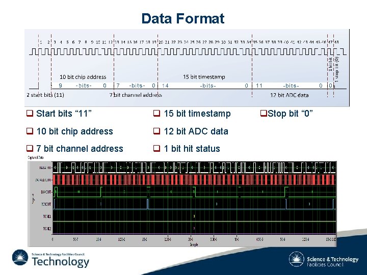
Data Format q Start bits “ 11” q 15 bit timestamp q 10 bit chip address q 12 bit ADC data q 7 bit channel address q 1 bit hit status q. Stop bit “ 0”

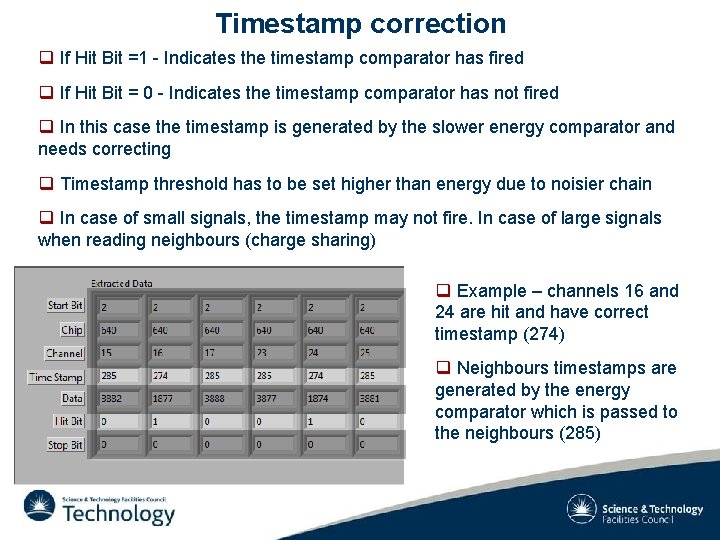
Timestamp correction q If Hit Bit =1 - Indicates the timestamp comparator has fired q If Hit Bit = 0 - Indicates the timestamp comparator has not fired q In this case the timestamp is generated by the slower energy comparator and needs correcting q Timestamp threshold has to be set higher than energy due to noisier chain q In case of small signals, the timestamp may not fire. In case of large signals when reading neighbours (charge sharing) q Example – channels 16 and 24 are hit and have correct timestamp (274) q Neighbours timestamps are generated by the energy comparator which is passed to the neighbours (285)

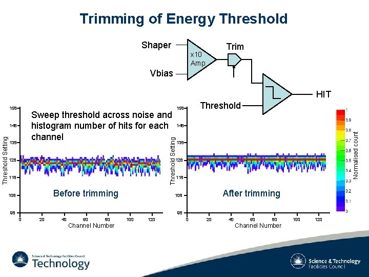
Trimming of Energy Threshold Shaper Trim x 10 Amp Vbias HIT Sweep threshold across noise and histogram number of hits for each channel 148 Threshold Setting 148 Threshold 158 Normalised count 158 138 128 118 Before trimming 108 After trimming 108 98 98 0 20 40 60 80 Channel Number 100 120

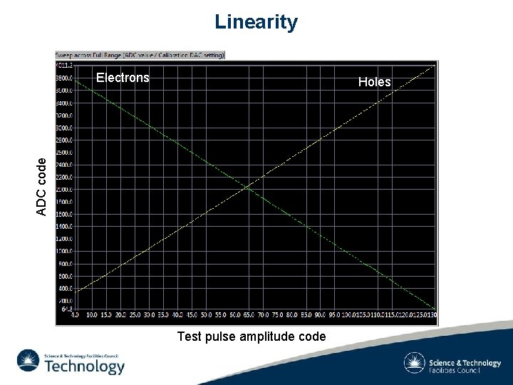
Linearity Electrons ADC code Holes Test pulse amplitude code

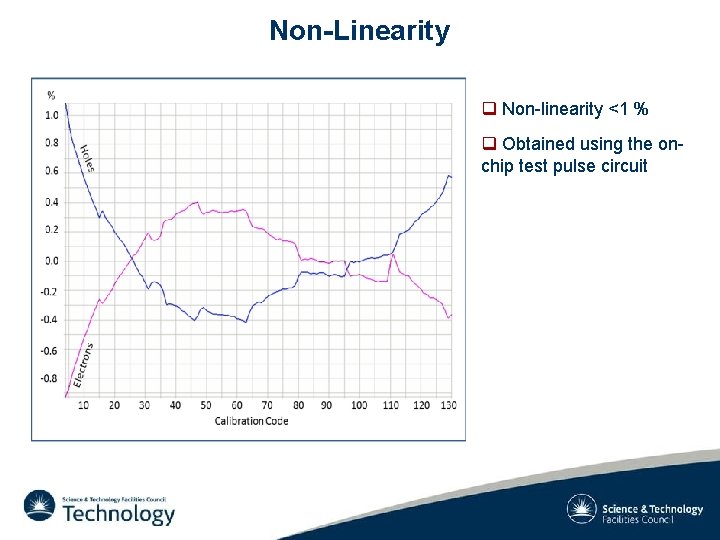
Non-Linearity q Non-linearity <1 % q Obtained using the onchip test pulse circuit

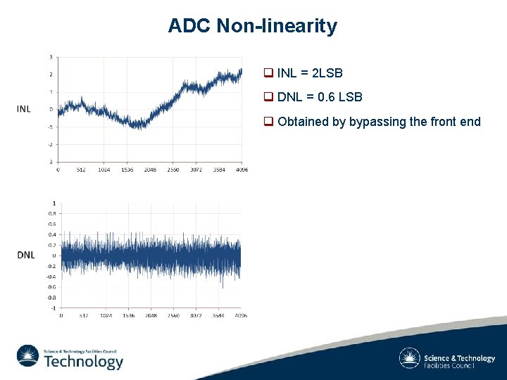
ADC Non-linearity q INL = 2 LSB q DNL = 0. 6 LSB q Obtained by bypassing the front end

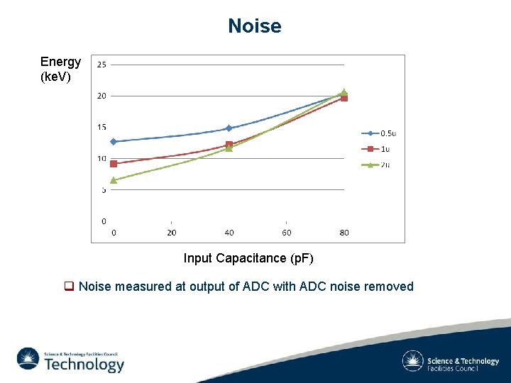
Noise Energy (ke. V) Input Capacitance (p. F) q Noise measured at output of ADC with ADC noise removed

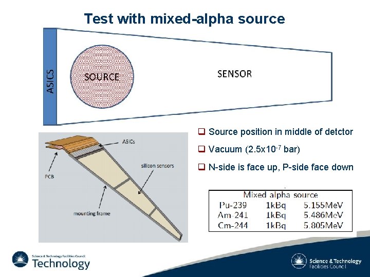
Test with mixed-alpha source q Source position in middle of detctor q Vacuum (2. 5 x 10 -7 bar) q N-side is face up, P-side face down

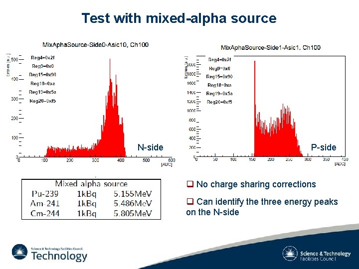
Test with mixed-alpha source N-side P-side q No charge sharing corrections q Can identify the three energy peaks on the N-side

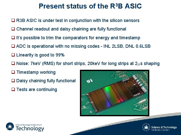
Present status of the R 3 B ASIC q R 3 B ASIC is under test in conjunction with the silicon sensors q Channel readout and daisy chaining are fully functional q It’s possible to trim the comparators for energy and timestamp q ADC is operational with no missing codes - INL 2 LSB, DNL 0. 6 LSB q Linearity is good to 99% q Noise: 7 ke. V (RMS) for short strips, 20 ke. V for long strips at 2 ms shaping q Timestamp working q Daisy chaining fully functional q Tests are continuing

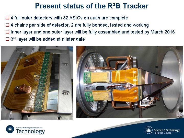
Present status of the R 3 B Tracker q 4 full outer detectors with 32 ASICs on each are complete q 4 chains per side of detector, 2 are fully bonded, tested and working q Inner layer and one outer layer will be fully assembled and tested by March 2016 q 3 rd layer will be added at a later date

Thank you for Listening Thanks to the R 3 B tracker collaboration Contact Details Lawrence Jones IC Design Engineer, ASIC Design Group Science and Technology Facilities Council Rutherford Appleton Laboratory, Harwell Campus, Didcot OX 11 0 QX United Kingdom Tel +44(0)1235 446508 Fax +44(0)1235 445008 Email: lawrence. jones@stfc. ac. uk