8421 BCD 4 0 9 0 0000 8421
Sign up to view full document!
SIGN UP
![](https://slidetodoc.com/presentation_image_h2/9bd95de04584e86a6d80ae41be7276ca/image-1.jpg)
![](http://slidetodoc.com/presentation_image_h2/9bd95de04584e86a6d80ae41be7276ca/image-2.jpg)
![](http://slidetodoc.com/presentation_image_h2/9bd95de04584e86a6d80ae41be7276ca/image-3.jpg)
![电路设计要求 十�制数 8421 BCD� ■ 4个输入信号表示 0 ~ 9 0 0000 ■ 使用 8421 电路设计要求 十�制数 8421 BCD� ■ 4个输入信号表示 0 ~ 9 0 0000 ■ 使用 8421](http://slidetodoc.com/presentation_image_h2/9bd95de04584e86a6d80ae41be7276ca/image-4.jpg)
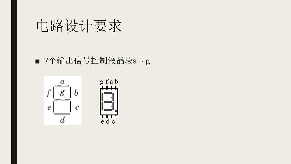
电路设计要求 十�制数 8421 BCD� ■ 4个输入信号表示 0 ~ 9 0 0000 ■ 使用 8421 BCD码 1 0001 2 0010 3 0011 4 0100 5 0101 6 0110 7 0111 8 1000 9 1001
![](http://slidetodoc.com/presentation_image_h2/9bd95de04584e86a6d80ae41be7276ca/image-5.jpg)
![](http://slidetodoc.com/presentation_image_h2/9bd95de04584e86a6d80ae41be7276ca/image-6.jpg)
![电路设计 if input = 0 then turn on a, b, c, d, e, f 电路设计 if input = 0 then turn on a, b, c, d, e, f](http://slidetodoc.com/presentation_image_h2/9bd95de04584e86a6d80ae41be7276ca/image-7.jpg)
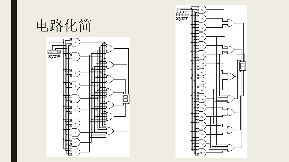
电路设计 if input = 0 then turn on a, b, c, d, e, f endif if input = 1 then turn on b, c endif. . .
![电路设计 if input = 0, 2, 3, 5, 6, 7, 8, 9 then turn 电路设计 if input = 0, 2, 3, 5, 6, 7, 8, 9 then turn](http://slidetodoc.com/presentation_image_h2/9bd95de04584e86a6d80ae41be7276ca/image-8.jpg)
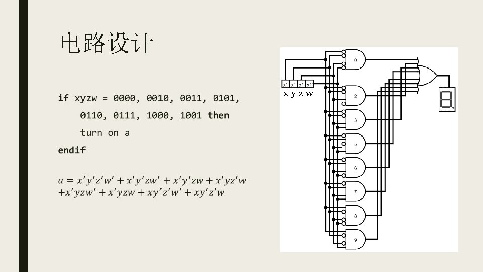
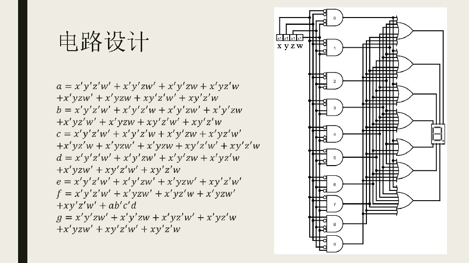
电路设计 if input = 0, 2, 3, 5, 6, 7, 8, 9 then turn on a endif if input = 0, 1, 2, 3, 4, 7, 8, 9 then turn on b endif. . .
![](http://slidetodoc.com/presentation_image_h2/9bd95de04584e86a6d80ae41be7276ca/image-9.jpg)
![](http://slidetodoc.com/presentation_image_h2/9bd95de04584e86a6d80ae41be7276ca/image-10.jpg)
![](http://slidetodoc.com/presentation_image_h2/9bd95de04584e86a6d80ae41be7276ca/image-11.jpg)
![](http://slidetodoc.com/presentation_image_h2/9bd95de04584e86a6d80ae41be7276ca/image-12.jpg)
![](http://slidetodoc.com/presentation_image_h2/9bd95de04584e86a6d80ae41be7276ca/image-13.jpg)
![](http://slidetodoc.com/presentation_image_h2/9bd95de04584e86a6d80ae41be7276ca/image-14.jpg)
![电路再化简 十�制数 8421 BCD� 0 0000 1 0001 2 0010 3 0011 4 0100 电路再化简 十�制数 8421 BCD� 0 0000 1 0001 2 0010 3 0011 4 0100](http://slidetodoc.com/presentation_image_h2/9bd95de04584e86a6d80ae41be7276ca/image-15.jpg)
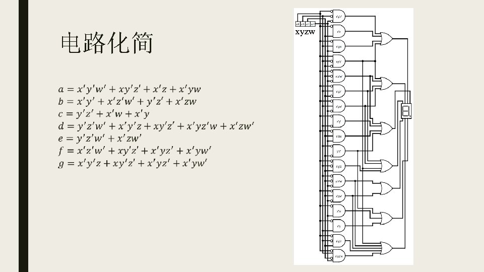
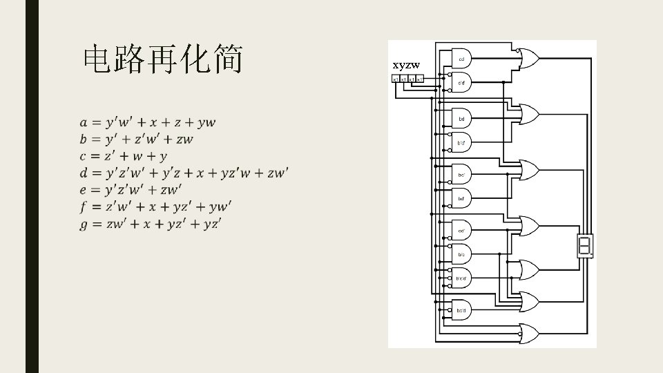
电路再化简 十�制数 8421 BCD� 0 0000 1 0001 2 0010 3 0011 4 0100 5 0101 6 0110 7 0111 8 1000 9 1001 zw=11 10 01 00 xy=11 abcdefg = xxxxxxx 10 xxxxxxx 1111011 1111111 01 1110000 1011111 1011011 0110011 00 1111001 1101101 0110000 1111110
![电路再化简 ■ zw zw ’ z’w’ xy 0/1 0/1 xy’ 0/1 1 1 x’y 电路再化简 ■ zw zw ’ z’w’ xy 0/1 0/1 xy’ 0/1 1 1 x’y](http://slidetodoc.com/presentation_image_h2/9bd95de04584e86a6d80ae41be7276ca/image-16.jpg)
电路再化简 ■ zw zw ’ z’w’ xy 0/1 0/1 xy’ 0/1 1 1 x’y 1 1 1 0 x’y’ 1 1 0 1
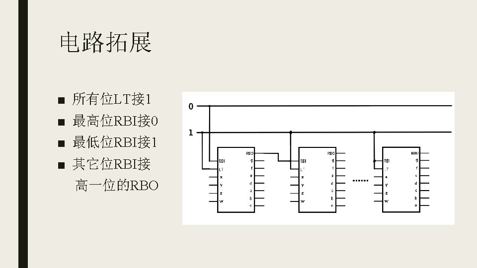
![](http://slidetodoc.com/presentation_image_h2/9bd95de04584e86a6d80ae41be7276ca/image-17.jpg)
![](http://slidetodoc.com/presentation_image_h2/9bd95de04584e86a6d80ae41be7276ca/image-18.jpg)
![](http://slidetodoc.com/presentation_image_h2/9bd95de04584e86a6d80ae41be7276ca/image-19.jpg)
![电路拓展 ■ RBI xyzw RBO 电路拓展 ■ RBI xyzw RBO](http://slidetodoc.com/presentation_image_h2/9bd95de04584e86a6d80ae41be7276ca/image-20.jpg)
电路拓展 ■ RBI xyzw RBO
![](http://slidetodoc.com/presentation_image_h2/9bd95de04584e86a6d80ae41be7276ca/image-21.jpg)
![LT 电路拓展 ■ RBI xyzw RBO LT 电路拓展 ■ RBI xyzw RBO](http://slidetodoc.com/presentation_image_h2/9bd95de04584e86a6d80ae41be7276ca/image-22.jpg)
LT 电路拓展 ■ RBI xyzw RBO
![](http://slidetodoc.com/presentation_image_h2/9bd95de04584e86a6d80ae41be7276ca/image-23.jpg)
![](http://slidetodoc.com/presentation_image_h2/9bd95de04584e86a6d80ae41be7276ca/image-24.jpg)
- Slides: 24