825 1 U SAR T INTRODUCTION USART Universal


 Bidirectional data bus •")
 “Active low“ terminal which receives a signal for")
 Indicates that the 8251 is ready to accept")
 Indicates that the 8251 contains a character that")
 Input port for MODEM interface. • DTR (Output")


 output is switched to logic 1 level to tell")

- Slides: 20
825 1 U SAR T
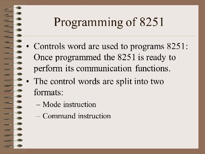
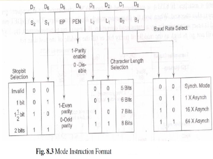
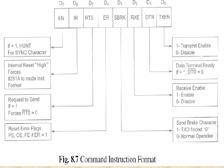
INTRODUCTION • USART -Universal Synchronous Asynchronous Receiver Transmitter • Packaged in a 28 -pin DIP by Intel • Serial data communication • Receives parallel data, transmits serial data • Receives serial, transmits parallel data
PIN DIAGRAM
PIN DESCRIPTION • D 0 to D 7 (l/O terminal) Bidirectional data bus • RESET (Input terminal) A "High" on this input forces the 8251 into "reset status. " • CLK (Input terminal) Used to generate internal device timing. CLK signal is independent of RXC or TXC. • WR (Input terminal) “Active low" input terminal which receives a signal for writing transmit data and control words from the CPU into the 8251.
PIN DESCRIPTION • RD (Input terminal) “Active low“ terminal which receives a signal for reading received data and status words from 8251. • C/D (Input terminal) Receives a signal for selecting data(C/D=low) or command words and status words(C/D=high) when 8251 is accessed by the CPU. • CS (Input terminal) “Active low" terminal which selects 8251 at low level when the CPU accesses. • TXD (output terminal) Used for transmitting data from which serial-converted data is sent out. The device is in "mark status" (high level) after resetting.
PIN DESCRIPTION • TXRDY (output terminal) Indicates that the 8251 is ready to accept a transmitted data character. • TXEMPTY (Output terminal) Indicates that the 8251 has transmitted all the characters and had no data character. • TXC (Input terminal) Clock input signal which determines the transfer speed of transmitted data. Falling edge of TXC shifts the serial data out of the 8251. • RXD (input terminal) The terminal which receives serial data.
PIN DESCRIPTION • RXRDY (Output terminal) Indicates that the 8251 contains a character that is ready to READ. • RXC (Input terminal) Clock input signal which determines the transfer speed of received data. • SYNDET/BD (Input or output terminal) Internal synchronous mode (high-sync characters are received and synchronized) External synchronous mode-input terminal (High-receive data characters). Asynchronous mode-output terminal
PIN DESCRIPTION • DSR (Input terminal) Input port for MODEM interface. • DTR (Output terminal) Output port for MODEM interface. • CTS (Input terminal) Active low input terminal for MODEM interface which is used for controlling a transmit circuit. • RTS (Output terminal) Output port for MODEM interface.
SYNCHRONOUS COMMUNICATION • Clock signal is present between two microprocessor systems. • Each block of data has synch characters. The size of block data can be 100 or more bytes. Transmit data Receive data System 1 clk Signal common System 2
ASYNCHRONOUS COMMUNICATION • Eliminates the need for a clock signal between two microprocessor based systems. • Data to be transmitted is sent out one character at a time. Transmit data Receive data System 1 Signal common System 2
BLOCK DIAGRAM
BLOCK DIAGRAM Sections of 8251 USART: • Read/Write control logic • Transmitter • Receiver • Data bus system • Modem control
TRANSMITTER • Transmitter section receives parallel data from the microprocessor over the data bus. The character is then automatically framed with the start bit, parity bit, correct number of stop bits, and put into the transmit data buffer register. • Finally, it is shifted out of this register to produce a bit serial output on the Tx. D line.
TRANSMITTER • Tx. RDY is switched to logic 1 when the transmit buffer register is empty. • Tx. E transmitter Empty –This is an output signal. Logic 1 on this line indicates the output register is empty. Reset when a byte is transferred from the buffer to output registers. • Tx. C Transmitter Clock Controls the rate by which bits are transmitted by the USART. The clock can be set to 1, 16 or 64 times the baud.
RECEIVER • The receiver section: whenever Rx. D line goes low, control assumes it is a start bit, waits for half bit time and samples again. • Responsible for reading the serial bit stream of data at Rx. D(received data) input and converting it into parallel form.
RECEIVER • Rx. RDY(receive ready) output is switched to logic 1 level to tell the microprocessor that a char is available and is sitting inside the USART and should be read from the receive –buffer register. • Rx. C Receiver Clock controls the rate by which bits are received by the USART. In Asynchronous Mode, the clock can be set to 1, 16 or 64 times the baud.
8251 A STATUS WORD