8086 PROCESSOR UNIT IB Mr S VINOD ASSISTANT

8086 PROCESSOR UNIT I-B Mr. S. VINOD ASSISTANT PROFESSOR EEE DEPARTMENT

8086 PROCESSOR --Functional block diagram --Signals --Memory interfacing --I/O ports and data transfer concepts --Timing Diagram --Interrupt structure.
 • It is a 16 bit μp. • 8086")
8086 Microprocessor (cont. . ) • It is a 16 bit μp. • 8086 has a 20 bit address bus can access up to memory locations ( 1 MB). • It can support up to 64 K I/O ports. • It provides 14, 16 -bit registers. • It has multiplexed address and data bus AD 0 AD 15 and A 16 – A 19.
 • It requires single phase clock with 33% duty")
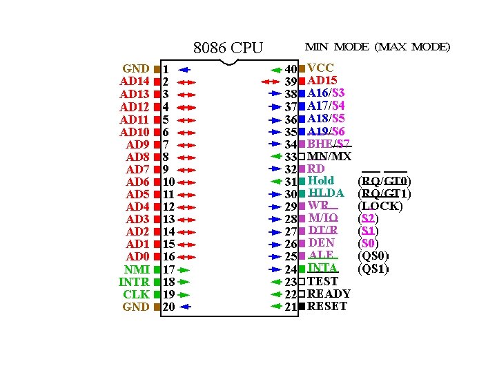
8086 Microprocessor (cont. . ) • It requires single phase clock with 33% duty cycle to provide internal timing. • 8086 is designed to operate in two modes, Minimum and Maximum. • It can pre fetches up to 6 instruction bytes from memory and queues them in order to speed up instruction execution. • It requires +5 V power supply. • A 40 pin dual in line package.
 • Minimum and Maximum Modes: • The minimum mode")
8086 Microprocessor (cont. . ) • Minimum and Maximum Modes: • The minimum mode is selected by applying logic 1 to the MN / MX# input pin. This is a single microprocessor configuration. • The maximum mode is selected by applying logic 0 to the MN / MX# input pin. This is a multi micro processors configuration.

Signals
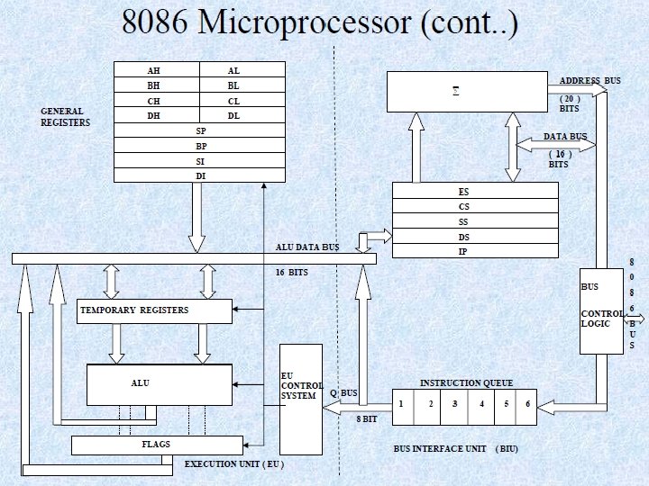
 8086 has two blocks BIU and EU.")
Internal Architecture of 8086 (cont. . ) 8086 has two blocks BIU and EU. • The BIU performs all bus operations such as instruction fetching, reading and writing operands for memory and calculating the addresses of the memory operands. • The instruction bytes are transferred to the instruction queue. • EU executes instructions from the instruction system byte queue. • Both units operate asynchronously to give the 8086 an overlapping instruction fetch and execution mechanism which is called as Pipelining. This results in efficient use of the system bus and system performance. • BIU contains Instruction queue, Segment registres, Instruction pointer, Address adder. • EU contains Control circuitry, Instruction decoder, ALU, Pointer and Index register, Flag register.
 Bus Interface Unit: • It provides a")
Internal Architecture of 8086 (cont. . ) Bus Interface Unit: • It provides a full 16 bit bidirectional data bus and 20 bit address bus. • The bus interface unit is responsible for performing all external bus operations. • Specifically it has the following functions: • Instruction fetch, Instruction queuing, Operand fetch and storage, Address relocation and Bus control. • The BIU uses a mechanism known as an instruction stream queue to implement a pipeline architecture.

• This queue permits pre fetch of up to six bytes of instruction code. When ever the queue of the BIU is not full, it has room for at least two more bytes and at the same time the EU is not requesting it to read or write operands from memory, the BIU is free to look ahead in the program by prefetching the next sequential instruction. • These prefetching instructions are held in its FIFO queue. With its 16 bit data bus, the BIU fetches two instruction bytes in a single memory cycle. • After a byte is loaded at the input end of the queue, it automatically shifts up through the FIFO to the empty location nearest the output.
 • The EU accesses the queue from")
Internal Architecture of 8086 (cont. . ) • The EU accesses the queue from the output end. It reads one instruction byte after the other from the output of the queue. If the queue is full and the EU is not requesting access to operand in memory. • These intervals of no bus activity, which may occur between bus cycles are known as Idle state. • If the BIU is already in the process of fetching an instruction when the EU request it to read or write operands from memory or I/O, the BIU first completes the instruction fetch bus cycle before initiating the operand read / write cycle.
 • The BIU also contains a dedicated")
Internal Architecture of 8086 (cont. . ) • The BIU also contains a dedicated adder which is used to generate the 20 bit physical address that is output on the address bus. This address is formed by adding an appended 16 bit segment address and a 16 bit offset address. • For example, the physical address of the next instruction to be fetched is formed by combining the current contents of the code segment CS register and the current contents of the instruction pointer IP register. • The BIU is also responsible for generating bus control signals such as those for memory read or write and I/O read or write.
 • EXECUTION UNIT : • The Execution")
Internal Architecture of 8086 (cont. . ) • EXECUTION UNIT : • The Execution unit is responsible for decoding and executing all instructions. • The EU extracts instructions from the top of the queue in the BIU, decodes them, generates operands if necessary, passes them to the BIU and requests it to perform the read or write bys cycles to memory or I/O and perform the operation specified by the instruction on the operands. • During the execution of the instruction, the EU tests the status and control flags and updates them based on the results of executing the instruction.
 • If the queue is empty, the")
Internal Architecture of 8086 (cont. . ) • If the queue is empty, the EU waits for the next instruction byte to be fetched and shifted to top of the queue. • When the EU executes a branch or jump instruction, it transfers control to a location corresponding to another set of sequential instructions. • Whenever this happens, the BIU automatically resets the queue and then begins to fetch instructions from this new location to refill the queue.
")
Internal Architecture of 8086 (cont. . )
")
Internal Architecture of 8086 (cont. . )
")
Internal Architecture of 8086 (cont. . )

Minimum Mode Interface • When the Minimum mode operation is selected, the 8086 provides all control signals needed to implement the memory and I/O interface. • The minimum mode signal can be divided into the following basic groups : address/data bus, status, control, interrupt and DMA. • Address/Data Bus : these lines serve two functions. As an address bus is 20 bits long and consists of signal lines A 0 through A 19 represents the MSB and A 0 LSB. A 20 bit address gives the 8086 a 1 Mbyte memory address space. More over it has an independent I/O address space which is 64 K bytes in length.
 • The 16 data bus lines D")
Minimum Mode Interface ( cont. . ) • The 16 data bus lines D 0 through D 15 are actually multiplexed with address lines A 0 through A 15 respectively. By multiplexed we mean that the bus work as an address bus during first machine cycle and as a data bus during next machine cycles. D 15 is the MSB and D 0 LSB. • When acting as a data bus, they carry read/write data for memory, input/output data for I/O devices, and interrupt type codes from an interrupt controller.
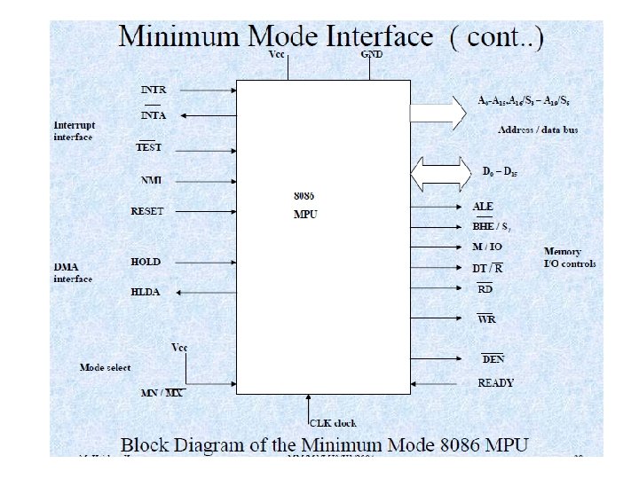
 • Status signal : The four most")
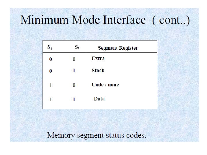
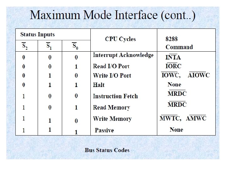
Minimum Mode Interface ( cont. . ) • Status signal : The four most significant address lines A 19 through A 16 are also multiplexed but in this case with status signals S 6 through S 3. These status bits are output on the bus at the same time that data are transferred over the other bus lines. • Bit S 4 and S 3 together from a 2 bit binary code that identifies which of the 8086 internal segment registers are used to generate the physical address that was output on the address bus during the current bus cycle. • Code S 4 S 3 = 00 identifies a register known as extra segment register as the source of the segment address.
 • Status line S 5 reflects the")
Minimum Mode Interface ( cont. . ) • Status line S 5 reflects the status of another internal characteristic of the 8086. It is the logic level of the internal enable flag. The last status bit S 6 is always at the logic 0 level. • Control Signals : The control signals are provided to support the 8086 memory I/O interfaces. They control functions such as when the bus is to carry a valid address in which direction data are to be transferred over the bus, when valid write data are on the bus and when to put read data on the system bus.
 • ALE is a pulse to logic")
Minimum Mode Interface ( cont. . ) • ALE is a pulse to logic 1 that signals external circuitry when a valid address word is on the bus. This address must be latched in external circuitry on the 1 -to-0 edge of the pulse at ALE. • Another control signal that is produced during the bus cycle is BHE bank high enable. Logic 0 on this used as a memory enable signal for the most significant byte half of the data bus D 8 through D 1. These lines also serves a second function, which is as the S 7 status line. • Using the M/IO and DT/R lines, the 8086 signals which type of bus cycle is in progress and in which direction data are to be transferred over the bus.

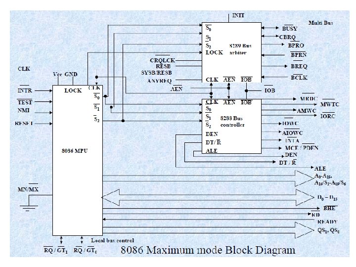
Maximum Mode Interface • When the 8086 is set for the maximum-mode configuration, it provides signals for implementing a multiprocessor / coprocessor system environment. • By multiprocessor environment we mean that one microprocessor exists in the system and that each processor is executing its own program. • Usually in this type of system environment, there are some system resources that are common to all processors. • They are called as global resources. There also other resources that are assigned to specific processors. These are known as local or private resources.
 • Coprocessor also means that there is a")
Maximum Mode Interface (cont. . ) • Coprocessor also means that there is a second processor in the system. In this two processor does not access the bus at the same time. • One passes the control of the system bus to the other and then may suspend its operation. • In the maximum-mode 8086 system, facilities are provided for implementing allocation of global resources and passing bus control to other microprocessor or coprocessor.

Internal Registers of 8086 • The 8086 has four groups of the user accessible internal registers. They are the instruction pointer, four data registers, four pointer and index register, four segment registers. • The 8086 has a total of fourteen 16 -bit registers including a 16 bit register called the status register, with 9 of bits implemented for status and control flags.
 • Most of the registers contain data/instruction")
Internal Registers of 8086 (cont. . ) • Most of the registers contain data/instruction offsets within 64 KB memory segment. There are four different 64 KB segments for instructions, stack, data and extra data. To specify where in 1 MB of processor memory these 4 segments are located the processor uses four segment registers: • Code segment (CS) is a 16 -bit register containing address of 64 KB segment with processor instructions. The processor uses CS segment for all accesses to instructions referenced by instruction pointer (IP) register. CS register cannot be changed directly. The CS register is automatically updated during far jump, far call and far return instructions.
 • Stack segment (SS) is a 16")
Internal Registers of 8086 (cont. . ) • Stack segment (SS) is a 16 -bit register containing address of 64 KB segment with program stack. By default, the processor assumes that all data referenced by the stack pointer (SP) and base pointer (BP) registers is located in the stack segment. SS register can be changed directly using POP instruction. • Data segment (DS) is a 16 -bit register containing address of 64 KB segment with program data. By default, the processor assumes that all data referenced by general registers (AX, BX, CX, DX) and index register (SI, DI) is located in the data segment. DS register can be changed directly using POP and LDS instructions.
 • Extra segment (ES) is a 16")
Internal Registers of 8086 (cont. . ) • Extra segment (ES) is a 16 -bit register containing address of 64 KB segment, usually with program data. By default, the processor assumes that the DI register references the ES segment in string manipulation instructions. ES register can be changed directly using POP and LES instructions. • It is possible to change default segments used by general and index registers by prefixing instructions with a CS, SS, DS or ES prefix. • All general registers of the 8086 microprocessor can be used for arithmetic and logic operations. The general registers are:
 • Accumulator register consists of two 8")
Internal Registers of 8086 (cont. . ) • Accumulator register consists of two 8 -bit registers AL and AH, which can be combined together and used as a 16 - bit register AX. AL in this case contains the low-order byte of the word, and AH contains the high-order byte. Accumulator can be used for I/O operations and string manipulation. • Base register consists of two 8 -bit registers BL and BH, which can be combined together and used as a 16 bit register BX. BL in this case contains the low-order byte of the word, and BH contains the high-order byte. BX register usually contains a data pointer used for based, based indexed or register indirect addressing.
 • Count register consists of two 8")
Internal Registers of 8086 (cont. . ) • Count register consists of two 8 -bit registers CL and CH, which can be combined together and used as a 16 -bit register CX. When combined, CL register contains the low-order byte of the word, and CH contains the high order byte. Count register can be used in Loop, shift/rotate instructions and as a counter in string manipulation, . • Data register consists of two 8 -bit registers DL and DH, which can be combined together and used as a 16 -bit register DX. When combined, DL register contains the low-order byte of the word, and DH contains the high order byte. Data register can be used as a port number in I/O operations. In integer 32 -bit multiply and divide instruction the DX register contains highorder word of the initial or resulting number.

• Addressing modes – Register and immediate modes we have already seen MOV AX, 1 MOV BX, AX register immediate

3 F 03 - 80 x 86 assembler • Typical addressing modes – Absolute address mode MOV AX, [0200] value stored in memory location DS: 0200

3 F 03 - 80 x 86 assembler • Typical addressing modes – Register indirect MOV AX, [BX] value stored at address contained in DS: BX

3 F 03 - 80 x 86 assembler • Typical addressing modes – Displacement MOV DI, 4 MOV AX, [0200+DI] value stored at DS: 0204

3 F 03 - 80 x 86 assembler • Typical addressing modes – Indexed MOV BX, 0200 MOV DI, 4 MOV AX, [BX+DI] value stored at DS: 0204

3 F 03 - 80 x 86 assembler • Typical addressing modes – Memory indirect MOV DI, 0204 MOV BX, [DI] MOV AX, [BX] If DS: 0204 contains 0256, then AX will contain whatever is stored at DS: 0256

3 F 03 - 80 x 86 assembler • Typical addressing modes – Memory indirect MOV DI, 0204 MOV BX, [DI] MOV AX, [BX] If DS: 0204 contains 0256, then AX will contain whatever is stored at DS: 0256

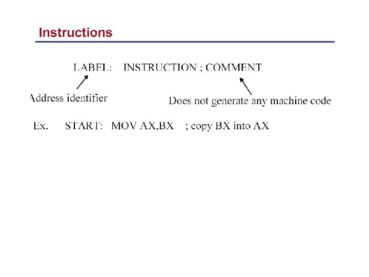
8086 Instruction - Example Label Operator INIT: mov Label Operator Operands Comment ax, bx - Operand[s] ; Comment ; Copy contents of bx into ax INIT: mov ax and bx alphanumeric string between ; and n • Not case sensitive • Unlike other assemblers, destination operand is first • mov is the mnemonic that the assembler translates into an opcode

Assembler Language Segment Types • Stack – For dynamic data storage – Source file defines size • Data – For static data Storage – Source file defines size – Source file defines content • Code – For machine Instructions
 CBW CWD IN LAHF LDS LEA LES")
x 86 Instruction Set Summary (Data Transfer) CBW CWD IN LAHF LDS LEA LES LODS MOVS OUT POPF PUSHF SAHF STOS XCHG XLAT ; Convert Byte to Word AL AX ; Convert Word to Double in AX DX, AX ; Input ; Load AH from Flags ; Load pointer to DS ; Load EA to register ; Load pointer to ES ; Load memory at SI into AX ; Move memory at SI to DI ; Output ; Pop Flags ; Push Flags ; Store AH into Flags ; Store AX into memory at DI ; Exchange ; Translate byte to AL
 AAA AAD AAM AAS ADC ADD AND CMC CMPS")
86 Instruction Set Summary (Arithmetic/Logical) AAA AAD AAM AAS ADC ADD AND CMC CMPS DAA DAS DEC DIV IDIV MUL INC ; ASCII Adjust for Add in AX ; ASCII Adjust for Divide in AX ; ASCII Adjust for Multiply in AX ; ASCII Adjust for Subtract in AX ; Add with Carry ; Add ; Logical AND ; Complement Carry ; Compare memory at SI and DI ; Decimal Adjust for Add in AX ; Decimal Adjust for Subtract in AX ; Decrement ; Divide (unsigned) in AX(, DX) ; Divide (signed) in AX(, DX) ; Multiply (unsigned) in AX(, DX) ; Multiply (signed) in AX(, DX) ; Increment
 NOT OR RCL Left RCR Right ROL")
86 Instruction Set Summary (Arithmetic/Logical Cont. ) NOT OR RCL Left RCR Right ROL ROR SAR SBB SUB TEST XOR ; Logical NOT ; Logical inclusive OR ; Rotate through Carry ; Rotate Left ; Rotate Right ; Shift Arithmetic Right ; Subtract with Borrow ; Subtract ; AND function to flags ; Logical Exclusive OR
 CALL CLC CLI HLT INTO IRET JB/JNAE")
86 Instruction Set Summary (Control/Branch Cont. ) CALL CLC CLI HLT INTO IRET JB/JNAE JBE/JNA JCXZ JE/JZ JL/JNGE JLE/JNG JMP JNB/JAE JNBE/JA JNE/JNZ JNL/JGE ; Call ; Clear Carry ; Clear Interrupt ; Halt ; Interrupt on Overflow ; Interrupt Return ; Jump on Below/Not Above or Equal ; Jump on Below or Equal/Not Above ; Jump on CX Zero ; Jump on Equal/Zero ; Jump on Less/Not Greater or Equal ; Jump on Less or Equal/Not Greater ; Unconditional Jump ; Jump on Not Below/Above or Equal ; Jump on Not Below or Equal/Above ; Jump on Not Equal/Not Zero ; Jump on Not Less/Greater or Equal

x 86 Instruction Set Summary JNLE/JG JNO JNP/JPO JNS JO JP/JPE JS LOCK LOOPNZ/LOOPNE LOOPZ/LOOPE NOP REP/REPNE/REPNZ REPE/REPZ RET SEG STC STD STI TEST WAIT (Control/Branch) ; Jump on Not Less or Equal/Greater ; Jump on Not Overflow ; Jump on Not Parity/Parity Odd ; Jump on Not Sign ; Jump on Overflow ; Jump on Parity/Parity Even ; Jump on Sign ; Bus Lock prefix ; Loop CX times ; Loop while Not Zero/Not Equal ; Loop while Zero/Equal ; No Operation (= XCHG AX, AX) ; Repeat/Repeat Not Equal/Not Zero ; Repeat Equal/Zero ; Return from call ; Segment register ; Set Carry ; Set Direction ; Set Interrupt ; AND function to flags ; Wait
 dd define double word")
Assembler Directives db define byte dw define word (2 bytes) dd define double word (4 bytes) dq define quadword (8 bytes) dt define tenbytes equate, assign numeric expression to a name Examples: db 100 dup (? ) define 100 bytes, with no initial values for bytes db “Hello” define 5 bytes, ASCII equivalent of “Hello”. maxint equ 32767 count 10 * 20 equ ; calculate a value (200)

16 -Bit Additions Address Label 1000 Mnemonic MVI SI, 1500 Opcode C 6 1001 C 7 1002 00 1003 15 1004 MOV AX, [SI] 1005 04 8 B 1006 MOV CX, 0000 C 1 1007 C 7 1008 00 1009 00 100 A ADD AX, [SI+02] 44 100 B 03 100 C 02 100 D 01 100 E 73 100 F 1010 : CX 41 MOV SI, 1700 67 1011 C 7 1012 00 1013 17 1014 MOV[SI], AX 1015 1016 04 89 MOV[SI+02], CX 4 C 1017 89 1018 02 1019 HLT F 4 Comment

Address Label 1000 16 -Bit Subtraction Mnemonic MVI SI, 1400 Opcode C 6 1001 C 7 1002 00 1003 14 1004 MOV AX, [SI] 1005 04 8 B 1006 MOV CX, 0000 C 1 1007 C 7 1008 00 1009 00 100 A SUB AX, [SI+02] 44 100 B 2 B 100 C 02 100 D 01 100 E 73 100 F 1010 : CX 41 MOV SI, 1600 67 1011 C 7 1012 00 1013 16 1014 MOV[SI], AX 1015 1016 04 89 MOV[SI+02], CX 4 C 1017 89 1018 02 1019 HLT F 4 Comment

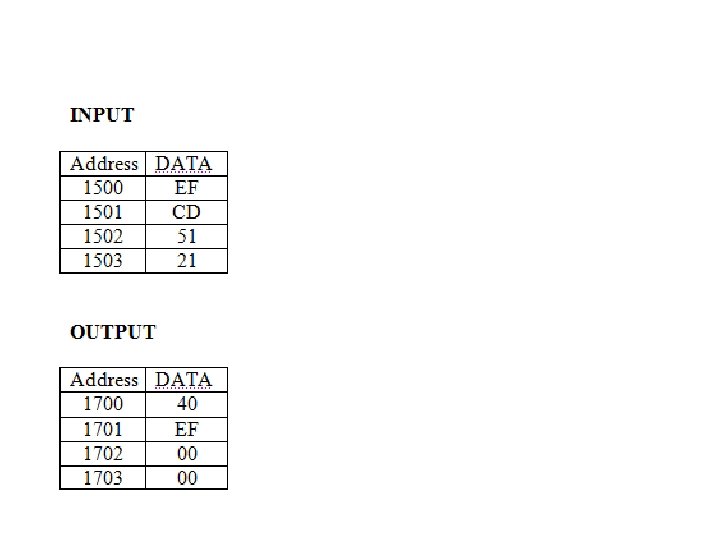
16 -Bit Multiplication Address Mnemonic 1000 MVI SI, 1500 Opcode C 6 1001 C 7 1002 00 1003 15 1004 MOV AX, 000 F 5 C 1005 8 B 1006 0 F 1007 1008 00 MOV BX, 0002 5 C 1009 8 B 100 A 02 100 B 00 100 C MUL BX 100 D F 7 100 E 100 F E 3 73 MOV SI, 1200 C 6 1010 C 7 1011 00 1012 1013 12 MOV[SI], AX 1014 04 89 1015 JNC SI 46 1016 JNC SI 46 1017 MOV AX, DX 00 1018 1019 89 MOV[SI], AX 101 A 101 B 04 89 HLT F 4

16 -Bit Division Address Mnemonic 1000 MVI SI, 1300 Opcode C 6 1001 C 7 1002 00 1003 13 1004 MOV AX, [SI] 1005 1006 04 8 B MOV BX, [SI+2] 5 C 1007 8 B 1008 02 1009 DIV BX 100 A 100 B F 3 F 7 MOV[SI+04] , AX 44 100 C 89 100 D 04 100 E MOV[SI+06] , DX 54 100 F 89 1010 06 1011 HLT F 4

Interrupts The processor has the following interrupts: • INTR is a maskable hardware interrupt. The interrupt can be enabled/disabled using STI/CLI instructions or using more complicated method of updating the FLAGS register with the help of the POPF instruction. • When an interrupt occurs, the processor stores FLAGS register into stack, disables further interrupts, fetches from the bus one byte representing interrupt type, and jumps to interrupt processing routine address of which is stored in location 4 * <interrupt type>. Interrupt processing routine should return with the IRET instruction.
 • NMI is a non-maskable interrupt. Interrupt is processed in")
Interrupts (cont. . ) • NMI is a non-maskable interrupt. Interrupt is processed in the same way as the INTR interrupt. The address of the NMI processing routine is stored in location 0008 h. • This interrupt has higher priority then the maskable interrupt. • Software interrupts can be caused by: • INT instruction - breakpoint interrupt. This is a type 3 interrupt. INT <interrupt number> instruction - any one interrupt from available 256 interrupts. • INTO instruction - interrupt on overflow
- Slides: 60