8085 Microprocessor Architecture Support Components Contents n Pin


 n 8085 has 8")
 n Accumulator and Flag")


 1. Memory-mapped I/O (16 -bit address) 2.")


")

")

- Slides: 43
8085 Microprocessor: Architecture & Support Components
Contents n Pin diagram of 8085 n 8085 Operations n Architecture of 8085 n 8085 Communication with Memory
Pinout Diagram of 8085 n A 40 -pin IC n Six groups of signals n Address Bus n Data Bus n Control and Status pins n Power Supply & frequency signals n Externally initiated Signals n Serial I/O ports
Serial I/O ports Externally initiated signals Control & Status Address Bus Power Supply & frequency Data Bus Logic Pinout of 8085 Control & Status
8085 Operations n Microprocessor Initiated Operations n Internal Operations n Peripheral/Externally Initiated Operations
Microprocessor Initiated Operations n Memory Read n Memory Write n I/O Read n I/O Write
Internal Operations n Store 8 -bit data n Perform Arithmetic and Logic Operations n Test for conditions n Sequence the execution of instructions n Store/Retrieve data from stack during execution
Peripheral/Externally Initiated Operations n Reset n Interrupt n Ready n Hold
Architecture of 8085 n Power Supply – a +5 V DC power supply n Maximum clock frequency of 3 MHz n 8 -bit general purpose microprocessor n 16 -bit Address Bus n Capable of addressing 64 K of memory
Architecture of 8085
Architecture 0 f 8085 Cont… n ALU n Interrupt Control n Timing and Control Unit n Serial I/O Control n General Purpose n Address Bus n n Registers Program Status word Program Counter Stack Pointer Instruction Register and Decoder n Data Bus
Architecture 0 f 8085 Cont… n Arithmetic Logic Unit (ALU) n 8085 has 8 -bit ALU n Performs arithmetic & Logic operations on data n Timing & Control Unit n Generates timing and control signals n General Purpose Registers n 8 -bit registers (B, C, D, E, H, L) n 16 -bit register pairs (BC, DE, HL, PSW)
Architecture 0 f 8085 Cont… n Program Status Word (PSW) n Accumulator and Flag Register can be combined as a register pair called PSW n Instruction Register and Decoder n Instruction fetched from memory is stored in Instruction register (8 -bit register) n Decoder decodes the instruction and directs the Timing & Control Unit accordingly
Architecture 0 f 8085 Cont… n Interrupt Control n 8085 has 5 interrupt signals n n n INTR – general purpose interrupt RST 5. 5 Restart Interrupts RST 6. 5 RST 7. 5 TRAP – non-maskable interrupt The interrupts listed above are in increasing order of priority
Architecture 0 f 8085 Cont… n Serial I/O Control n 8085 has two signals for serial communication n SID – Serial Input Data n SOD – Serial Output Data
Architecture 0 f 8085 Cont… n Address Bus n Used to address memory & I/O devices n 8085 has a 16 -bit address bus Higher-order Address Lower-order Address A 15 A 14 A 13 A 12 A 11 A 10 A 9 A 8 AD 7 AD 6 AD 5 AD 4 AD 3 AD 2 AD 1 AD 0 Data Bus n Used to transfer instructions and data n 8085 has a 8 -bit data bus
8085 Communication with Memory n Involves the following three steps 1. Identify the memory location (with address) 2. Generate Timing & Control signals 3. Data transfer takes place
Example: Memory Read Operation 1 3 2
1 3 2
Timing Diagram
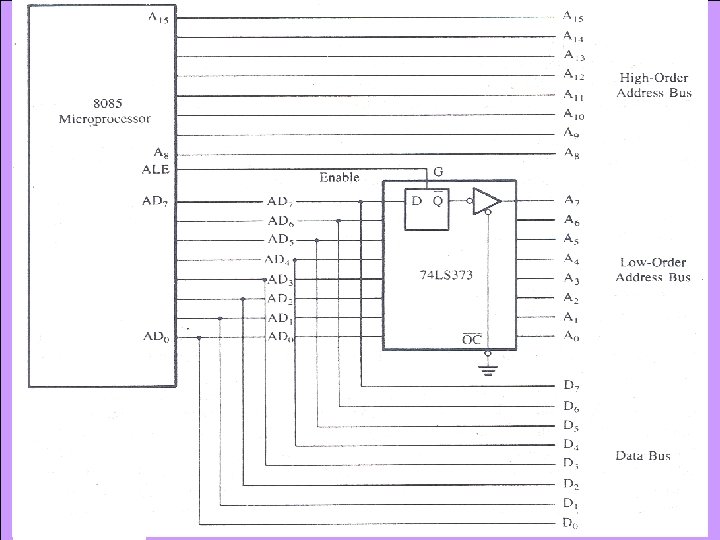
Demultiplexing Address/Data Bus n 8085 identifies a memory location with its 16 address lines, (AD 0 to AD 7) & (A 8 to A 15) n 8085 performs data transfer using its data lines, AD 0 to AD 7 n Lower order address bus & Data bus are multiplexed on same lines i. e. AD 0 to AD 7. n Demultiplexing refers to separating Address & Data signals for read/write operations
Need for Demultiplexing… RD A 8 -A 15 20 H AD 0 -AD 7 8085 05 H Memory 4 FH 2005 H
8085 Interfacing with Memory chips Address 8085 Data Address Memory Data Interface Control Memory Chip Control
8085 Interfacing with Memory chips Data 8085 Memory 74 LS 373 AD 0 -AD 7 A 0 – A 7 ALE A 8 -A 15 Control Memory Interface Chip
8085 Interfacing with Memory chips Data 8085 Program 74 LS 373 AD 0 -AD 7 A 0 – A 7 ALE A 8 -A 15 CS IO/M RD Memory Interface
Memory Mapping n 8085 has 16 -bit Address Bus n The complete address space is thus given by the range of addresses 0000 H – FFFFH n The range of addresses allocated to a memory device is known as its memory map
Memory map: 64 K memory device Address lines required: 16 (A 0 – A 15) n Memory map: 0000 H - FFFFH n So the memory map is n A 15 A 14 A 13 A 12 A 11 to A 0 0 0…. 0 0 0 to A 15 A 14 A 13 A 12 A 11 to A 0 1 1…. 111 1 = 0000 H = FFFFH
Interfacing I/O devices with 8085 Peripheral-mapped I/O & Memory-mapped I/O
Interfacing I/O devices with 8085 I/O Interface 8085 I/O Devices System Bus Memory Interface Memory Devices
Techniques for I/O Interfacing n Memory-mapped I/O n Peripheral-mapped I/O
Memory-mapped I/O n 8085 uses its 16 -bit address bus to identify a memory location n Memory address space: 0000 H to FFFFH n 8085 needs to identify I/O devices also n I/O devices can be interfaced using addresses from memory space n 8085 treats such an I/O device as a memory location n This is called Memory-mapped I/O
Peripheral-mapped I/O n 8085 has a separate 8 -bit addressing scheme for I/O devices n I/O address space: 00 H to FFH n This is called Peripheral-mapped I/O or mapped I/O-
8085 Communication with I/O devices n Involves the following three steps 1. Identify the I/O device (with address) 2. Generate Timing & Control signals 3. Data transfer takes place n 8085 communicates with a I/O device only if there is a Program Instruction to do so
1. Identify the I/O device (with address) 1. Memory-mapped I/O (16 -bit address) 2. Peripheral-mapped I/O (8 -bit address)
2. Generate Timing & Control Signals n Memory-mapped I/O n Reading Input: IO/M = 0, RD = 0 n Write to Output: IO/M = 0, WR = 0 n Peripheral-mapped I/O n Reading Input: IO/M = 1, RD = 0 n Write to Output: IO/M = 1, WR = 0 3. Data transfer takes place
Peripheral I/O Instructions n IN Instruction n Inputs data from input device into the accumulator n It is a 2 -byte instruction n Format: IN 8 -bit port address n Example: IN 01 H
n OUT Instruction n Outputs the contents of accumulator to an output device n It is a 2 -byte instruction n Format: OUT 8 -bit port address n Example: OUT 02 H
-----Example Program-----n WAP to read a number from input port (port address 01 H) and display it on ASCII display connected to output port (port address 02 H) IN 01 H ; reads data value 03 H (example)into ; accumulator, A = 03 H MVI B, 30 H; loads register B with 30 H ADD B ; A = 33 H, ASCII code for 3 OUT 02 H ; display 3 on ASCII display
Memory-mapped I/O Instructions n I/O devices are identified by 16 -bit addresses n 8085 communicates with an I/O device as if it were one of the memory locations n Memory related instructions are used n For e. g. LDA, STA n LDA 8000 H n Loads A with data read from input device with 16 -bit address 8000 H n STA 8001 H n Stores (Outputs) contents of A to output device with 16 -bit address 8001 H
-----Example Program-----n WAP to read a number from input port (port address 8000 H) and display it on ASCII display connected to output port (port address 8001 H) LDA 8000 H; reads data value 03 H (example)into ; accumulator, A = 03 H MVI B, 30 H; loads register B with 30 H ADD B ; A = 33 H, ASCII code for 3 STA 8001 H; display 3 on ASCII display
n Show the Pinout of 8085 in several grpups. n Mention the operations of 8085 in group n Discuss the data bus and address bus and the multiplexing. n Short questions