8051 ADDRESSING MODES Addressing Modes The 8051 provides

 immediate")


 and a")

 number system 32 Unpacked BCD The lower 4 bits of")
 number system 33 Packed BCD A single byte has two")
 number system 34 There is a problem with adding BCD")
 number system 35 DA instruction MOV A, #47 H ;")


 provides the time of day")


 to ASCII conversion Many ADC (analog-to-digital converter) chips provide output data in")
- Slides: 59
8051 ADDRESSING MODES
Addressing Modes The 8051 provides a total of five distinct addressing modes. (1) immediate (2) register (3) direct (4) register indirect (5) indexed
Immediate addressing mode The operand comes immediately after the op-code. The immediate data must be preceded by the pound sign, "#".
Register addressing mode involves the use of registers to hold the data to be manipulated.
Direct addressing mode There are 128 bytes of RAM in the 8051. The RAM has been assigned addresses 00 to 7 FH. It is most often used to access RAM locations 30 - 7 FH. Registers can be accessed by the register names of R 0 - R 7 or equivalent RAM address. Special function registers can also be accessed by their address. s
Direct addressing mode The data is in a RAM memory location whose address is known, and this address is given as a part of the instruction.
Special Function Registers In the 8051, registers A, B, PSW, and DPTR are part of the group of registers commonly referred to as SFR. The SFR can be accessed by their names or by their addresses. For example, register A has address E 0 H and register B has been designated the address F 0 H.
SFR
SFR registers and their addresses
Stack and direct addressing mode Only direct addressing mode is allowed for push and POP instructions of the stack. PUSH A is invalid. Pushing the accumulator onto the stack must be coded as PUSH 0 E 0 H. POP 04 will pop the top of the stack into R 4 of bank 0.
Register indirect addressing mode A register is used as a pointer to the data. If the data is inside the CPU, only registers R 0 and R 1 are used for this purpose. R 2 - R 7 cannot be used to hold the address of an operand located in RAM. RO and R 1 must be preceded by the @ sign.
Limitation of register indirect addressing mode R 0 and R 1 are the only registers that can be used for pointers in register indirect addressing mode. Since R 0 and R l are 8 bits wide, their use is limited to accessing any information in the internal RAM. To access data stored in external RAM or in the code space of on-chip ROM, we need a 16 -bit pointer, the DPTR.
Indexed addressing mode and onchip ROM access The look-up table can be created in ROM to access frequently accessed elements. MOVC instruction is used to access data value in ROM. The "C" means code. MOVC A, @ A+DPTR The 16 -bit register DPTR and register A are used to form the address of the data element stored in on-chip ROM.
Example Program to get value from P 1 and send x 2 to P 2 continuously. MOV DPTR, #SQUARE_TABLE MOV A, #0 FFH MOV P 1, A BACK: MOV A, P 1 MOVC A, @A+DPTR MOV P 2, A SJMP BACK ORG 500 H SQUARE_TABLE: DB 0, 1, 4, 9, 16, 25, 36, 49, 64, 81
Indirect addressing mode and MOVX instruction External RAM memory is accessed by the MOVX instruction. For External memory all registers R 0, R 1, … R 7 can be used. MOVX A, @Rn MOVX @Rn, A MOVX A, @DPTR MOVX @DPTR, A All MOVX includes A register Rn can address 256 bytes DPTR can address 64 KB
BIT ADDRESSABILITY Many microprocessors such as the 386 or Pentium allow programs to access registers and I/0 ports in byte size only. To check a single bit of an I/0 port, have to read the entire byte first and then manipulate the whole byte with some logic instructions to get hold of the desired single bit. This is not the case with the 8051. One of the most important features of the 8051 is the ability to access the registers, RAM, and I/0 ports in bits instead of bytes. This is a very unique and powerful feature of 8051 microcontroller
BIT ADDRESSES FOR RAM Bit-addressable RAM Figure 5– 1 16 Bytes of Internal RAM. Note: They are both bit- and byte-accessible.
BIT INSTRUCTIONS OF RAM Bit-addressable RAM Table 5– 2 Single-Bit Instructions Eg: SETB 00 h ; Set the 0 th bit of RAM 20 H CLR 0 Fh ; clears the 7 th bit RAM 21 H JB 21 h, HERE ; Jumps to HERE if 1 st bit of RAM 24 H is equal to 1 JNB 21 h, THERE ; Jumps to HERE if 1 st bit of RAM 24 H is equal to 0
BIT ADDRESSES FOR I/O port bit addresses Figure 5– 2 SFR RAM Address (Byte and Bit)
BIT ADDRESSES FOR I/O Bit memory map Table 5– 3 Bit Addresses for All Ports Eg: CLR P 1. 1 SETB P 2. 6
BIT ADDRESSES FOR REGISTERS Registers bit-addressability Registers A, B, PSW, IP, IE, SCON, TCON are only bit addressability. Eg: SETB A. 2 CLR B. 6 CPL PSW. 3
22 THE 8051 INSTRUCTION SET
Instruction Groups 23 The instructions are grouped into 5 groups ◦ ◦ ◦ Data Transfer Arithmetic Logic Boolean Branching
Data Transfer Instructions 24 MOV 8 -bit data transfer for internal RAM and the SFR. MOV A, Rn MOV A, direct MOV A, @Ri MOV A, #data MOV Rn, A MOV direct, Rn MOV @Ri, A MOV @Ri, direct MOV @Ri, #data
Data Transfer Operations 25 MOV 1 -bit data transfer involving the CY flag MOV C, bit MOV P. 1, C MOV 16 -bit data transfer involving the DPTR MOV DPTR, #data
Data Transfer Instructions 26 MOVC Move Code Byte Load the accumulator with a byte from program memory. Must use indexed addressing MOVC A, @A+DPTR MOVC A, @A+PC
Data Transfer Instructions 27 MOVX Data transfer between the accumulator and a byte from external data memory. MOVX A, @Ri MOVX A, @DPTR MOVX @Ri, A MOVX @DPTR, A
Data Transfer Instructions 28 PUSH / POP Push and Pop a data byte onto the stack. The data byte is identified by a direct address from the internal RAM locations. PUSH POP DPL 40 H
Data Transfer Instructions 29 XCH Exchange accumulator and a byte variable XCH XCH A, Rn A, direct A, @Ri XCHD Exchange lower digit of accumulator with the lower digit of the memory location specified. XCHD A, @Ri The lower 4 -bits of the accumulator are exchanged with the lower 4 bits of the internal memory location identified indirectly by the index register. The upper 4 -bits of each are not modified.
Arithmetic Instructions 30 ADD ◦ 8 -bit addition between the accumulator (A) and a second operand. The result is always in the accumulator. The CY flag is set/reset appropriately. ADDC ◦ 8 -bit addition between the accumulator, a second operand the previous value of the CY flag. Useful for 16 -bit addition in two steps. The CY flag is set/reset appropriately.
Example – 16 -bit Addition 31 Add 1 E 44 H to 56 CAH CLR C ; Clear the CY flag MOV A, 44 H ; The lower 8 -bits of the 1 st number ADD A, CAH ; The lower 8 -bits of the 2 nd number MOV R 1, A ; The result 0 EH will be in R 1. CY = 1. MOV A, 1 EH ; The upper 8 -bits of the 1 st number ADDC A, 56 H ; The upper 8 -bits of the 2 nd number MOV R 2, A ; The result of the addition is 75 H The overall result: 750 EH will be in R 2: R 1. CY = 0.
BCD (binary coded decimal) number system 32 Unpacked BCD The lower 4 bits of the number represent the BCD number. The rest of the bits are 0. For example, "0000 1001" IS unpacked BCD for 9 Unpacked BCD requires 1 byte of memory or an 8 -bit register to contain it.
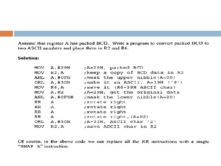
BCD (binary coded decimal) number system 33 Packed BCD A single byte has two BCD numbers. One in the lower 4 bits, and one in the upper 4 bits. For example, "0101 1001" is packed BCD for 59 H. It takes only 1 byte of memory to store the packed BCD operands. Its more efficient than unpacked BCD.
BCD (binary coded decimal) number system 34 There is a problem with adding BCD numbers. Adding two BCD numbers must give a BCD result. After adding packed BCD numbers, the result is no longer BCD. MOV A, #47 H ADD A, #25 H hexadecimal Addition will be 6 C BCD addition should be 72 "DA A" is designed to correct the BCD addition problem. 0110 1100 + 0110 --------
BCD (binary coded decimal) number system 35 DA instruction MOV A, #47 H ; A=47 H first BCD operand MOV B, #25 H ; B=25 second BCD operand ADD A, B ; hex (binary) addition (A=6 CH) DA A ; adjust for BCD addition (A=72 H) DAA must be used after the addition of BCD operands. DAA works only after an ADD instruction, it will not work after the INC instruction. DAA add 6 with the result of addition to get the valid BCD result. DAA will work only with accumulator.
Arithmetic Instructions 36 SUBB ◦ Subtract with Borrow. Subtract an operand the previous value of the borrow (carry) flag from the accumulator. A - <operand> - CY. The result is always saved in the accumulator. The CY flag is set/reset appropriately. A
Example – BCD addition 37 Add 34 to 49 BCD CLR C ; Clear the CY flag MOV A, #34 H ; Place 1 st number in A ADD A, #49 H ; Add the 2 nd number. ; A = 7 DH DA A ; A = 83 H
Arithmetic Instructions 38 INC ◦ Increment the operand by one. The operand can be a register, a direct address, an indirect address, the data pointer. DEC ◦ Decrement the operand by one. The operand can be a register, a direct address, an indirect address. MUL AB / DIV AB ◦ Multiply A by B and place result in A: B. ◦ Lower byte in A and upper byte in B ◦ Divide A by B and place result in A: B. ◦ Quotient in A and remainder in B
Logical Operations 39 ANL / ORL ◦ Work on byte sized operands or the CY flag. ANL A, Rn ANL A, direct ANL A, @Ri ANL A, #data ANL direct, A ANL direct, #data ANL C, 01 ANL C, P 3. 1
Logical Operations 40 XRL Works on bytes only. CPL / CLR Complement / Clear. Work on the accumulator or a bit. CLR P 1. 2 CLR A CPL B. 1
Logical Operations 41 RL / RLC / RRC ◦ Rotate the accumulator. RL and RR without the carry RLC and RRC rotate through the carry. SWAP A ◦ Swap the upper and lower nibbles of the accumulator. No compare instruction. ◦ Built into conditional branching instructions.
Boolean Operations 42 Manipulating the individual bits of bit addressable registers and memory locations as well as the CY flag. ◦ The P, OV, and AC flags cannot be directly altered. This group includes: ◦ ◦ Set, clear, and, or complement, move. Conditional jumps.
Boolean Operations 43 CLR ◦ Clear a bit or the CY flag. CLR P 1. 1 CLR C SETB ◦ Set a bit or the CY flag. SETB A. 2 SETB C CPL ◦ Complement a bit or the CY flag. CPL 40 H ; Complement bit 40 of the bit addressable memory
Boolean Operations 44 ORL / ANL ◦ OR / AND a bit with the CY flag. ORL C, 20 H ; OR bit 20 of bit addressable memory with the CY flag ANL C, 34 H ; AND complement of bit 34 of bit addressable memory with the CY flag. MOV ◦ Data transfer between a bit and the CY flag. MOV C, 3 FH ; Copy the CY flag to bit 3 F of the bit addressable memory. MOV P 1. 2, C ; Copy the CY flag to bit 2 of P 1.
Boolean Operations 45 JC / JNC ◦ Jump to a relative address if CY is set / cleared. JB / JNB ◦ Jump to a relative address if a bit is set / cleared. JB A. 2, <label> JBC ◦ ◦ Jump to a relative address if a bit is set and clear the bit. JBC B. 2, HERE
Packed BCD to ASCII conversion A real-time clock (RTC) provides the time of day and the date in packed BCD. Data to be displayed on a device such as an LCD, or to be printed by the printer, it must be in ASCII format. To convert packed BCD to ASCII, first convert to unpacked BCD. Add 30 to the unpacked BCD to get ASCII equivalent
ASCII to packed BCD conversion Keyboard key gives ASCII values. To manipulate the values from keyboard convert it into packed BCD First converted to unpacked BCD Then combined to make packed BCD. For example, for 4 and 7 the keyboard gives 34 and 37, respectively. The goal is to produce 47 H or “ 0100 0111″, which is packed BCD.
ASCII to packed BCD conversion
Branching Instructions 50 Four different types of unconditional jump instructions: Short Jump – SJMP Uses an 8 -bit signed offset relative to the 1 st byte of the next instruction. Long Jump – LJMP Uses a 16 -bit address. 3 byte instruction capable of referencing any location in the entire 64 K of program memory. Eg: SJMP SHORTJUMP LJMP LONGJUMP
Branching Instructions 51 Absolute Jump – AJMP Uses an 11 -bit address. 2 byte instruction The upper 3 -bits of the address combine with the 5 -bit opcode to form the 1 st byte and the lower 8 -bits of the address form the 2 nd byte. The 11 -bit address is substituted for the lower 11 -bits of the PC to calculate the 16 -bit address of the target. The location referenced must be within the 2 K Byte memory page containing the AJMP instruction. Indirect Jump – JMP @A + DPTR
Branching Instructions 52 5 different conditional jump instructions. ◦ ALL conditional jump instructions use an 8 -bit signed offset. ◦ Jump on Zero – JZ / JNZ Jump The ◦ ◦ if the A == 0 / A != 0 check is done at the time of the instruction execution. Eg: JNZ NEXT Jump on Carry – JC / JNC Jump if the C flag is set / cleared. Eg: JC AGAIN
Branching Instructions 53 Jump on Bit – JB / JNB Jump if the specified bit is set / cleared. Any addressable bit can be specified. Jump if the Bit is set then Clear the bit – JBC Jump if the specified bit is set. Then clear the bit. JB 21 h, HERE ; Jumps to HERE if 1 st bit of RAM 24 H is equal to 1 JNB 21 h, THERE ; Jumps to HERE if 1 st bit of RAM 24 H is equal to 0
Branching Instructions 54 Compare and Jump if Not Equal – CJNE Compare the magnitude of the two operands and jump if they are not equal. The values are considered to be unsigned. The Carry flag is set / cleared appropriately. CJNE A, direct, rel CJNE A, #data, rel CJNE Rn, #data, rel CJNE @Ri, #data, rel Eg: CJNE A, R 2, here
Branching Instructions 55 Decrement and Jump if Not Zero – DJNZ ◦ Decrement the first operand by 1 and jump to the location identified by the second operand if the resulting value is not zero. DJNZ Rn, rel direct, rel Eg: DJNZ 04, here No Operation ◦ NOP
CALL instruction 56 Two forms for the ◦ Absolute Call – ACALL Uses an 11 -bit address similar to AJMP The subroutine must be within the same 2 K page. ◦ ◦ ◦ Long Call – LCALL Uses a 16 -bit address similar to LJMP The subroutine can be anywhere. Eg: ACALL ROUTINE 1 Both forms push the 16 -bit address of the next instruction on the stack and update the stack pointer.
Return instructions 57 ◦ Return from subroutine – RET Pop the return address from the stack and continue execution there. ◦ Return from ISR – RETI Pop the return address from the stack. Restore the interrupt logic to accept additional interrupts at the same priority level as the one just processed. Continue execution at the address retrieved from the stack.
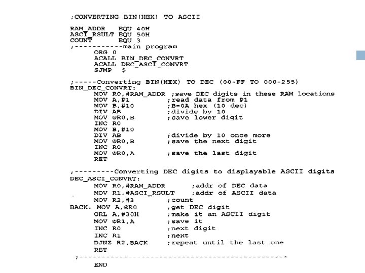
Binary (hex) to ASCII conversion Many ADC (analog-to-digital converter) chips provide output data in binary. To display the data on an LCD or PC screen, need to convert it to ASCII. Convert binary (hex) data init to decimal digits, Then converts the decimal digits to ASCII digits and saves them.