6 k 43 Gbs Differential TransimpedanceLimiting Amplifiers with
6 -k 43 -Gb/s Differential Transimpedance-Limiting Amplifiers with Auto-zero Feedback and High Dynamic Range H. Tran 1, F. Pera 2, D. S. Mc. Pherson 1, D. Viorel 1, and S. P. Voinigescu 3 1) Quake Technologies, Inc. Ottawa, ON, K 2 K 2 T 8, Canada 2) now with Insyte Corporation, Ottawa, ON, K 2 K 3 C 9, Canada 3) ECE Dept. , University of Toronto, ON, M 5 S 3 G 4, Canada
Outline Overview Broadband low-noise amplifier topologies and design methodology Circuit design and features Measurement results Summary M 3 Wednesday, November 12, 2003 Slide 2
Low-noise broadband amplifier topology Goals Minimize noise when circuit operated as TIA with 60 -f. F photodiode and As 50 - voltage preamplifier Maximise dynamic range by using on-chip active feedback that does not degrade overall noise. M 3 Wednesday, November 12, 2003 Slide 3
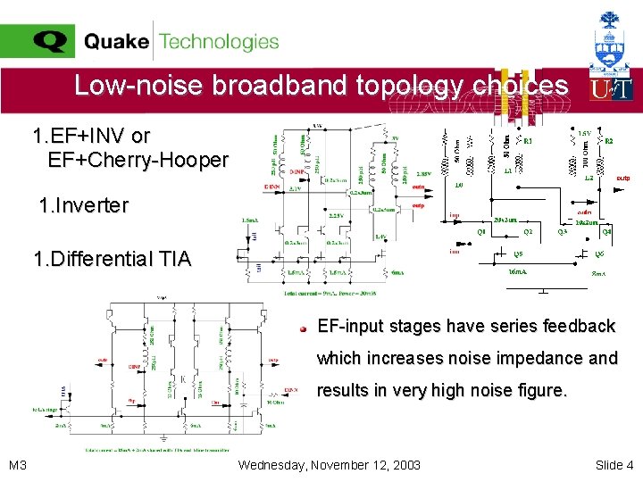
Low-noise broadband topology choices 1. EF+INV or EF+Cherry-Hooper 1. Inverter 1. Differential TIA EF-input stages have series feedback which increases noise impedance and results in very high noise figure. M 3 Wednesday, November 12, 2003 Slide 4
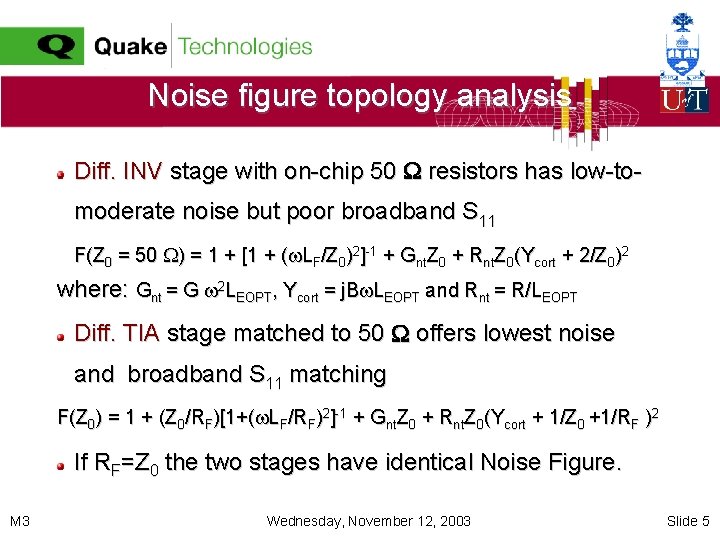
Noise figure topology analysis Diff. INV stage with on-chip 50 resistors has low-tomoderate noise but poor broadband S 11 F(Z 0 = 50 ) = 1 + [1 + (w. LF/Z 0)2]-1 + Gnt. Z 0 + Rnt. Z 0(Ycort + 2/Z 0)2 where: Gnt = G w 2 LEOPT, Ycort = j. Bw. LEOPT and Rnt = R/LEOPT Diff. TIA stage matched to 50 offers lowest noise and broadband S 11 matching F(Z 0) = 1 + (Z 0/RF)[1+(w. LF/RF)2]-1 + Gnt. Z 0 + Rnt. Z 0(Ycort + 1/Z 0 +1/RF )2 If RF=Z 0 the two stages have identical Noise Figure. M 3 Wednesday, November 12, 2003 Slide 5
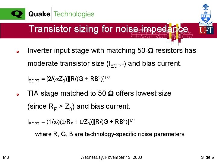
Transistor sizing for noise impedance Inverter input stage with matching 50 - resistors has moderate transistor size (l. EOPT) and bias current. l. EOPT = [2/(w. Z 0)][R/(G + RB 2)]1/2 TIA stage matched to 50 offers lowest size (since RF > Z 0) and bias current. l. EOPT = (1/w ( /RF + /Z 0)][R/(G + RB 2)]1/2 where R, G, B are technology-specific noise parameters M 3 Wednesday, November 12, 2003 Slide 6
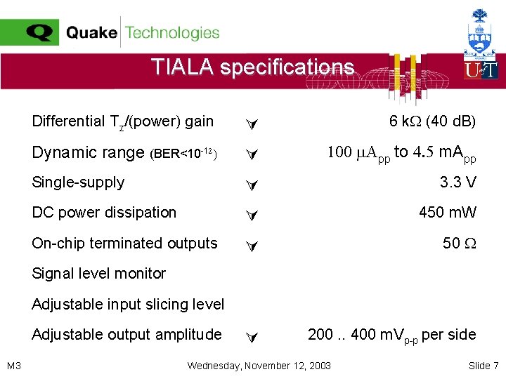
TIALA specifications Differential Tz/(power) gain 6 k (40 d. B) Dynamic range (BER<10 -1 pp to m. App Single-supply 3. 3 V DC power dissipation 450 m. W On-chip terminated outputs 50 200. . 400 m. Vp-p per side Signal level monitor Adjustable input slicing level Adjustable output amplitude M 3 Wednesday, November 12, 2003 Slide 7
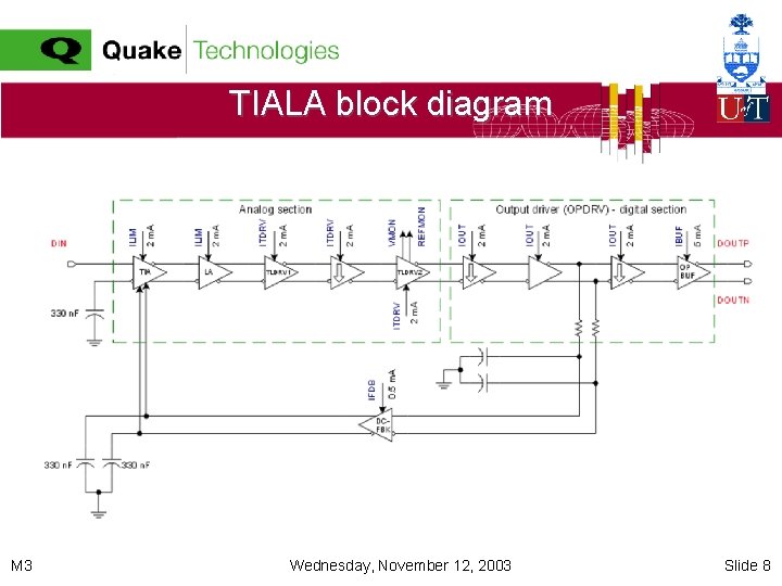
TIALA block diagram M 3 Wednesday, November 12, 2003 Slide 8
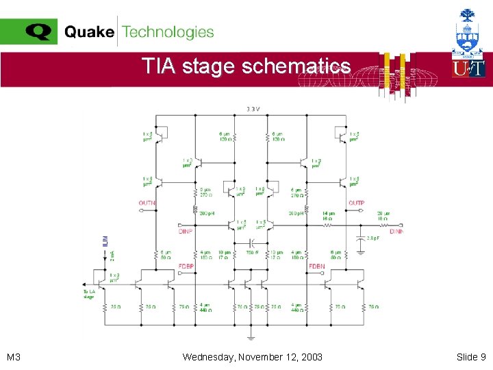
TIA stage schematics M 3 Wednesday, November 12, 2003 Slide 9
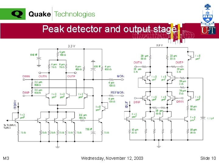
Peak detector and output stage M 3 Wednesday, November 12, 2003 Slide 10
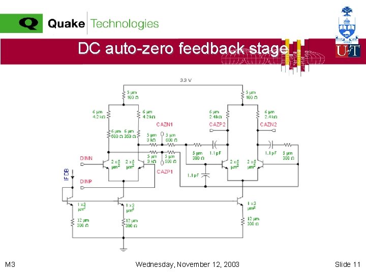
DC auto-zero feedback stage M 3 Wednesday, November 12, 2003 Slide 11
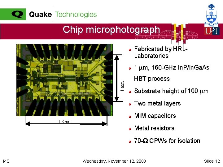
Chip microphotograph Fabricated by HRLLaboratories 1 mm 1 m, 160 -GHz In. P/In. Ga. As HBT process Substrate height of 100 m Two metal layers 1. 8 mm MIM capacitors Metal resistors 70 - CPWs for isolation M 3 Wednesday, November 12, 2003 Slide 12
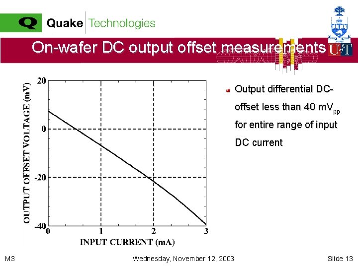
On-wafer DC output offset measurements Output differential DCoffset less than 40 m. Vpp for entire range of input DC current M 3 Wednesday, November 12, 2003 Slide 13
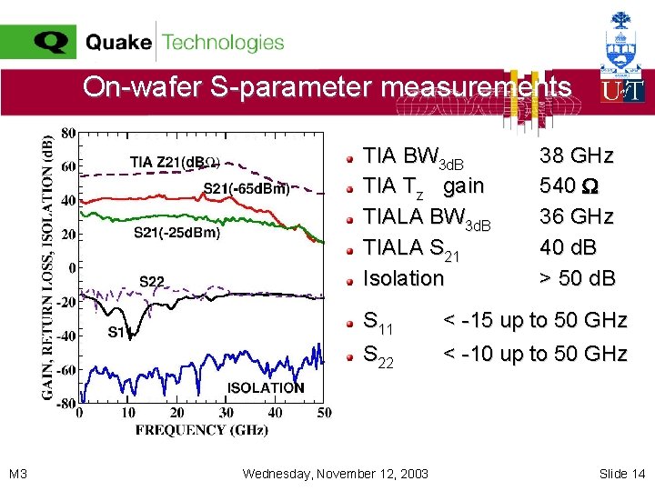
On-wafer S-parameter measurements TIA BW 3 d. B TIA Tz gain TIALA BW 3 d. B TIALA S 21 Isolation S 11 S 22 M 3 Wednesday, November 12, 2003 38 GHz 540 36 GHz 40 d. B > 50 d. B < -15 up to 50 GHz < -10 up to 50 GHz Slide 14
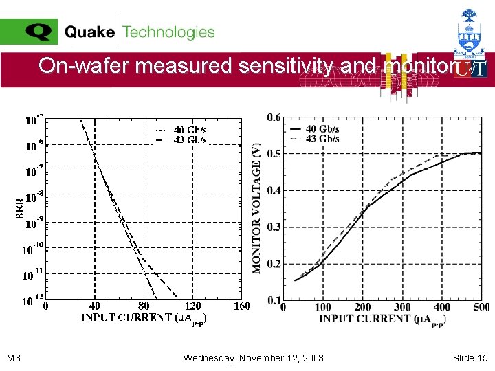
On-wafer measured sensitivity and monitor M 3 Wednesday, November 12, 2003 Slide 15
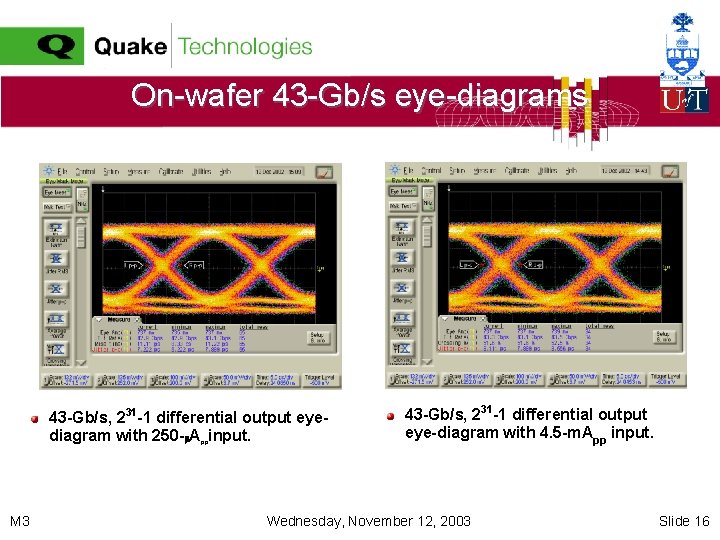
On-wafer 43 -Gb/s eye-diagrams 43 -Gb/s, 231 -1 differential output eyediagram with 250 - A input. pp M 3 43 -Gb/s, 231 -1 differential output eye-diagram with 4. 5 -m. App input. Wednesday, November 12, 2003 Slide 16
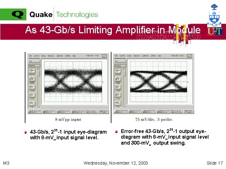
As 43 -Gb/s Limiting Amplifier in Module 43 -Gb/s, 231 -1 input eye-diagram with 8 -m. V input signal level. pp Error-free 43 -Gb/s, 231 -1 output eyediagram with 8 -m. V input signal level and 300 -m. V output swing. pp pp M 3 Wednesday, November 12, 2003 Slide 17
Summary A high dynamic range TIALA with on-chip auto-zero feedback was designed and fabricated in In. P/In. Ga. As HBT technology The input stage topology and design were optimized for broadband noise and input-impedance matching Signal monitor and slicing level adjust functions are incorporated The result is a unique circuit, with record functionality, that also operates as a 43 -Gb/s, 50 - matched voltage preamp or LA with record-breaking 8 -m. Vpp sensitivity M 3 Wednesday, November 12, 2003 Slide 18
Acknowledgment The authors would like to thank HRL-Laboratories for fabricating the die They would also like to express their gratitude to Quake colleagues M. Tazlauanu and S. Szilagyi for their valuable contributions M 3 Wednesday, November 12, 2003 Slide 19
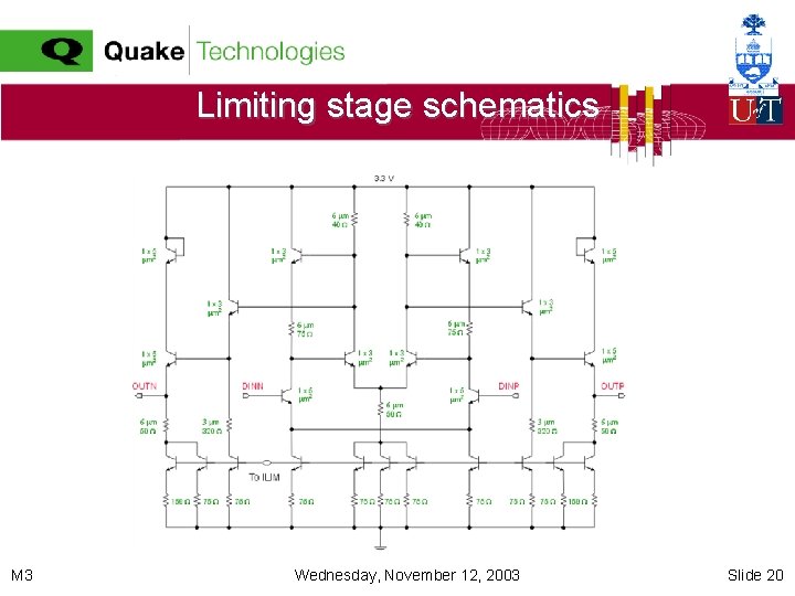
Limiting stage schematics M 3 Wednesday, November 12, 2003 Slide 20
Design overview On-chip auto-zero feedback for increased dynamic range Simultaneous noise- and input-impedance matching TIA and 2 nd. gain stage operate in linear mode Output stages operate in limiting mode Signal level monitor, slicing level adjust, and output swing control functions Based on a 1 - m In. P/In. Ga. As technology M 3 Wednesday, November 12, 2003 Slide 21
TIA stage design methodology Transistors biased @ 0. 6 m. A/ m 2 for minimum noise figure at 36 GHz, not for maximum gain/bandwidth Transistors sized such that the optimal noise impedance with feedback is close to 50 Inductors deployed in feedback network rather than in series with the loads for: improving S 11 over broader bandwidth, 3 -d. B bandwidth extension, and HF noise filtering. M 3 Wednesday, November 12, 2003 Slide 22
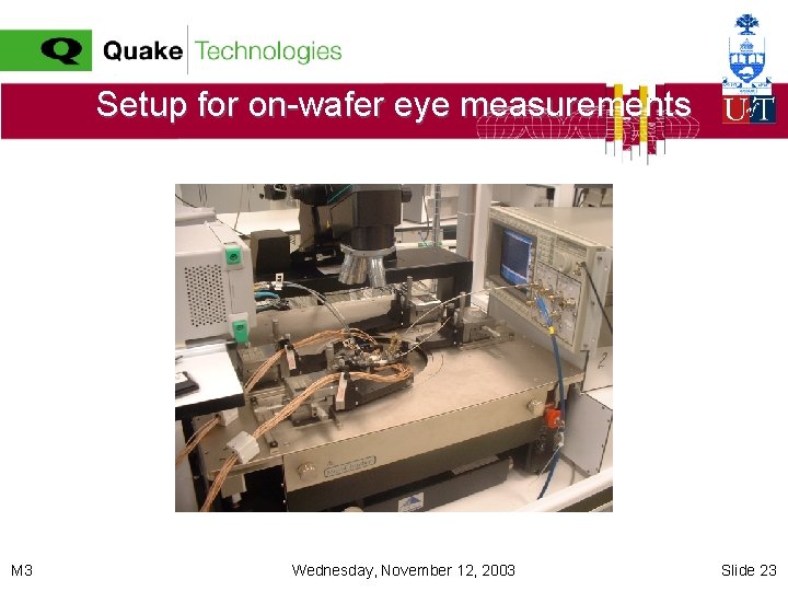
Setup for on-wafer eye measurements M 3 Wednesday, November 12, 2003 Slide 23
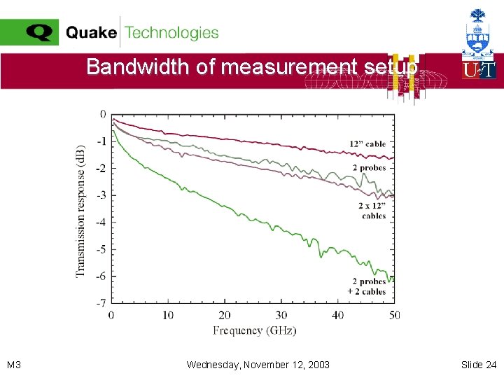
Bandwidth of measurement setup M 3 Wednesday, November 12, 2003 Slide 24
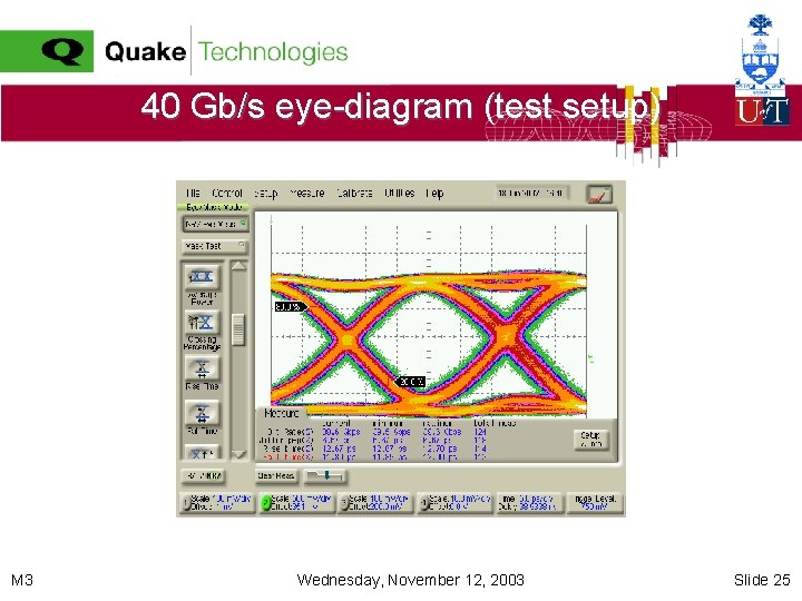
40 Gb/s eye-diagram (test setup) M 3 Wednesday, November 12, 2003 Slide 25
- Slides: 25