555 Timer Pin 5 Control Voltage A Worked

- Slides: 20

555 Timer - Pin 5 - Control Voltage - A Worked Example The following video is simply a series of slides, each displayed for about 5 seconds. Pause the slides as necessary. For quite a while I searched online for a hacked circuit which would take a pretty raw signal from an inductive pickup attached to an engines sparkplug lead, and convert it into a reliable pulse, capable of being used as a direct input to a microcontroller. I couldn’t anything that really helped me, so after gleaning bits and pieces from various places, I have finally got a circuit which works well for me. I don’t claim to know very much at all, so there may well be some geniuses who can look at what I have done and pick lots of holes in it. This video is not for them, and I expect it is far from perfect, but it is aimed at anyone who is in a similar place that I was, trying to get solution for this problem, but with no real success.

Shown above is the Fluke RPM 80 inductive pickup sensor, which when used with a Fluke 78 automotive multimeter or similar, can display an automotive engine’s cylinder sparking frequency, when hooked up to the engine sparkplug cable.

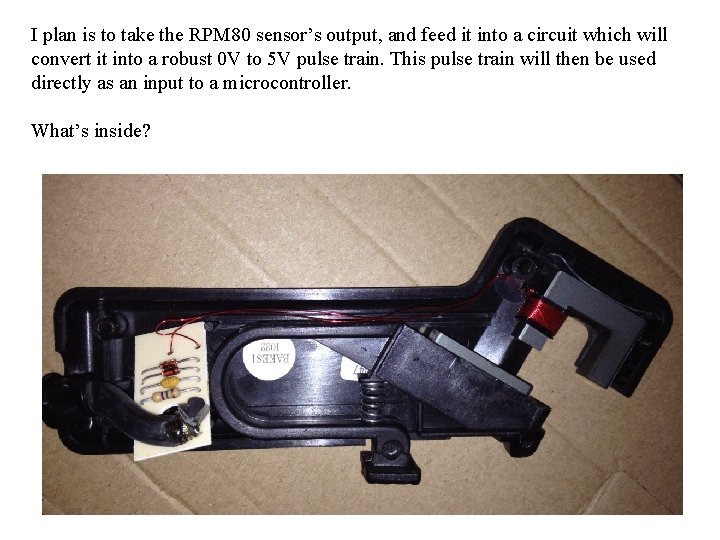
I plan is to take the RPM 80 sensor’s output, and feed it into a circuit which will convert it into a robust 0 V to 5 V pulse train. This pulse train will then be used directly as an input to a microcontroller. What’s inside?

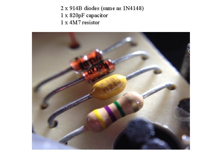
2 x 914 B diodes (same as 1 N 4148) 1 x 820 p. F capacitor 1 x 4 M 7 resistor

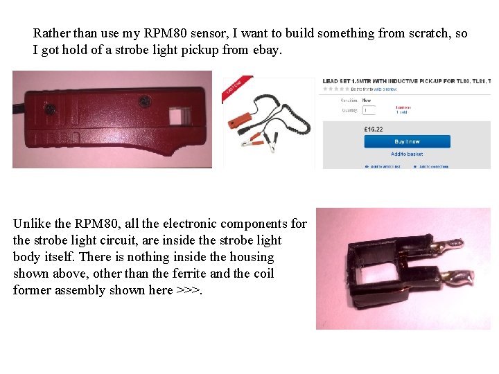
Rather than use my RPM 80 sensor, I want to build something from scratch, so I got hold of a strobe light pickup from ebay. Unlike the RPM 80, all the electronic components for the strobe light circuit, are inside the strobe light body itself. There is nothing inside the housing shown above, other than the ferrite and the coil former assembly shown here >>>.

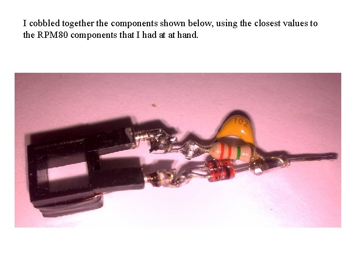
I cobbled together the components shown below, using the closest values to the RPM 80 components that I had at at hand.

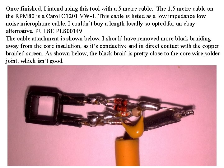
Once finished, I intend using this tool with a 5 metre cable. The 1. 5 metre cable on the RPM 80 is a Carol C 1201 VW-1. This cable is listed as a low impedance low noise microphone cable. I couldn’t buy a length locally so opted for an ebay alternative. PULSE PLS 00149 The cable attachment is shown below. I should have removed more black braiding away from the core insulation, as it’s conductive and in direct contact with the copper braided screen. As shown below, the black braid is pretty close to the core wire solder joint, which isn’t good.

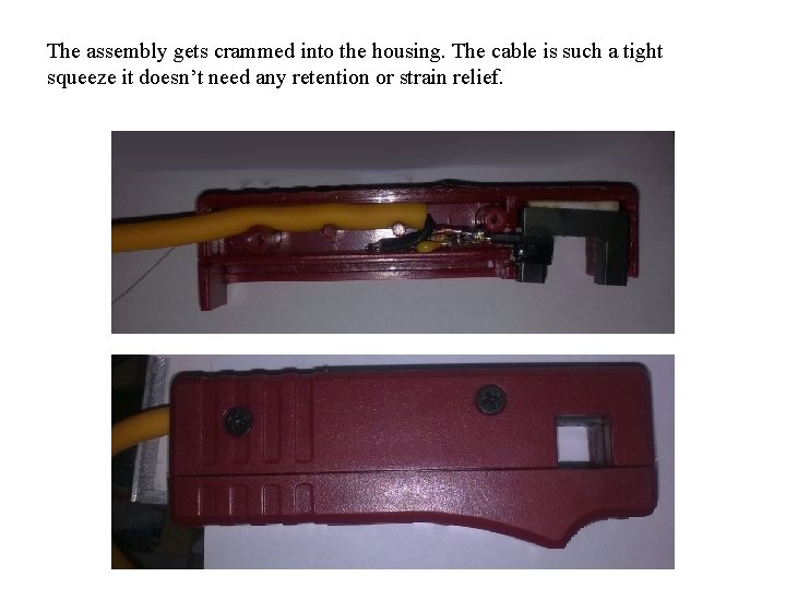
The assembly gets crammed into the housing. The cable is such a tight squeeze it doesn’t need any retention or strain relief.

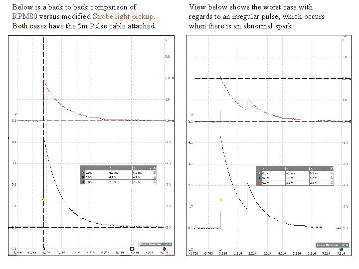
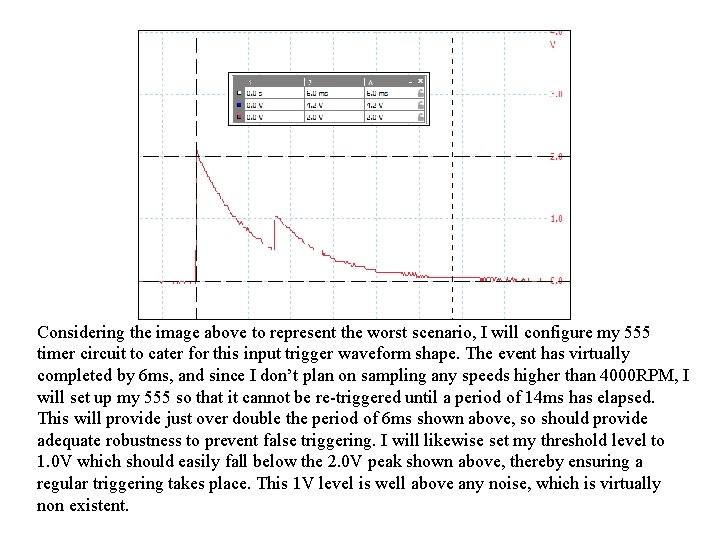
Below is a back to back comparison of RPM 80 versus modified Strobe light pickup. Both cases have the 5 m Pulse cable attached. View below shows the worst case with regards to an irregular pulse, which occurs when there is an abnormal spark.

Considering the image above to represent the worst scenario, I will configure my 555 timer circuit to cater for this input trigger waveform shape. The event has virtually completed by 6 ms, and since I don’t plan on sampling any speeds higher than 4000 RPM, I will set up my 555 so that it cannot be re-triggered until a period of 14 ms has elapsed. This will provide just over double the period of 6 ms shown above, so should provide adequate robustness to prevent false triggering. I will likewise set my threshold level to 1. 0 V which should easily fall below the 2. 0 V peak shown above, thereby ensuring a regular triggering takes place. This 1 V level is well above any noise, which is virtually non existent.

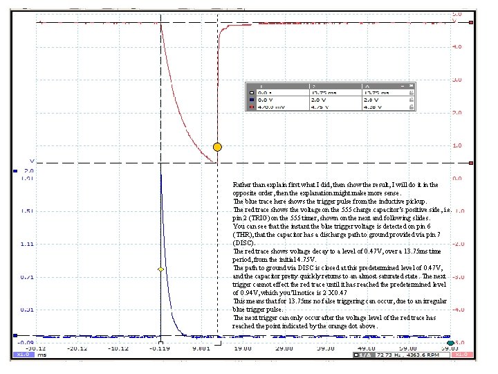
Rather than explain first what I did, then show the result, I will do it in the opposite order, then the explanation might make more sense. The blue trace here shows the trigger pulse from the inductive pickup. The red trace shows the voltage on the 555 charge capacitor’s positive side, i. e. pin 2 (TRIG) on the 555 timer, shown on the next and following slides. You can see that the instant the blue trigger voltage is detected on pin 6 (THR), that the capacitor has a discharge path to ground provided via pin 7 (DISC). The red trace shows voltage decay to a level of 0. 47 V, over a 13. 75 ms time period, from the initial 4. 75 V. The path to ground via DISC is closed at this predetermined level of 0. 47 V, and the capacitor pretty quickly returns to an almost saturated state. The next trigger cannot effect the red trace until it has reached the predetermined level of 0. 94 V, which you’ll notice is 2 X 0. 47 This means that for 13. 75 ms no false triggering can occur, due to an irregular blue trigger pulse. The next trigger can only occur after the voltage level of the red trace has reached the point indicated by the orange dot above.

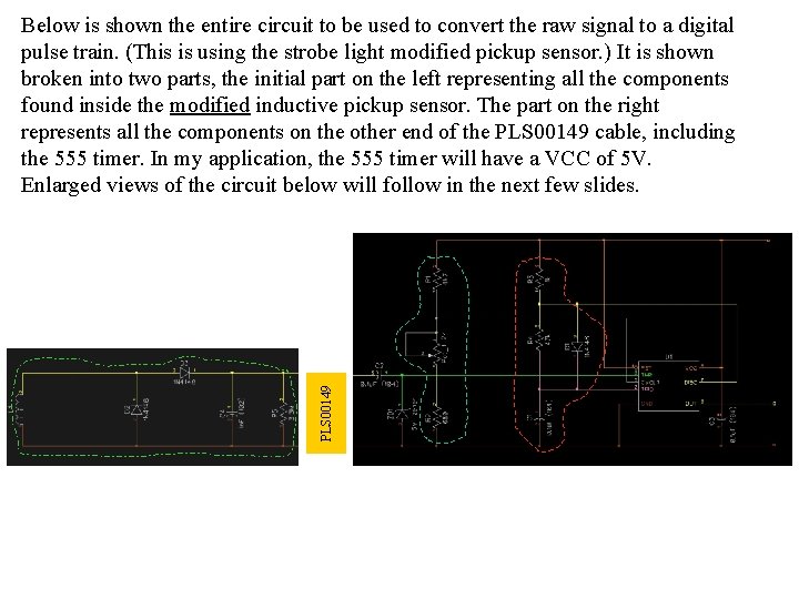
PLS 00149 Below is shown the entire circuit to be used to convert the raw signal to a digital pulse train. (This is using the strobe light modified pickup sensor. ) It is shown broken into two parts, the initial part on the left representing all the components found inside the modified inductive pickup sensor. The part on the right represents all the components on the other end of the PLS 00149 cable, including the 555 timer. In my application, the 555 timer will have a VCC of 5 V. Enlarged views of the circuit below will follow in the next few slides.

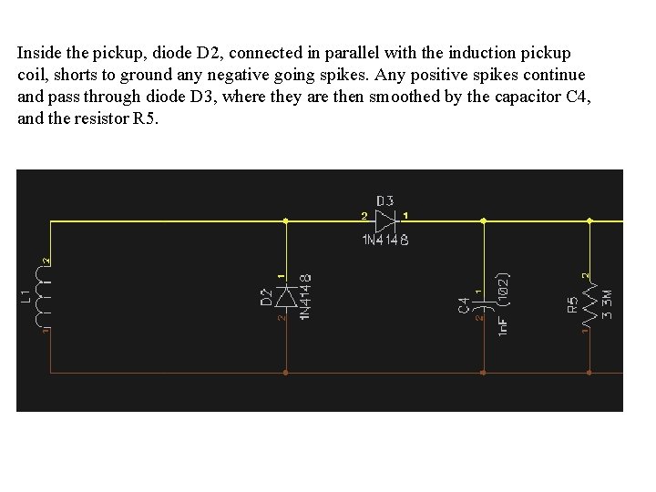
Inside the pickup, diode D 2, connected in parallel with the induction pickup coil, shorts to ground any negative going spikes. Any positive spikes continue and pass through diode D 3, where they are then smoothed by the capacitor C 4, and the resistor R 5.

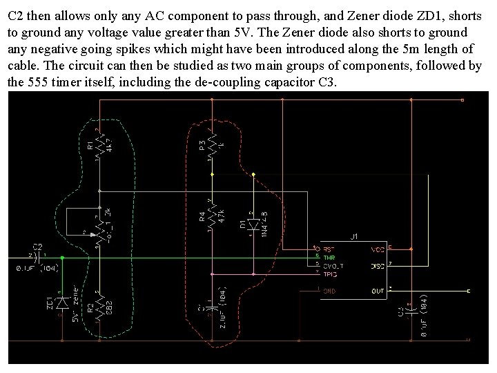
C 2 then allows only any AC component to pass through, and Zener diode ZD 1, shorts to ground any voltage value greater than 5 V. The Zener diode also shorts to ground any negative going spikes which might have been introduced along the 5 m length of cable. The circuit can then be studied as two main groups of components, followed by the 555 timer itself, including the de-coupling capacitor C 3.

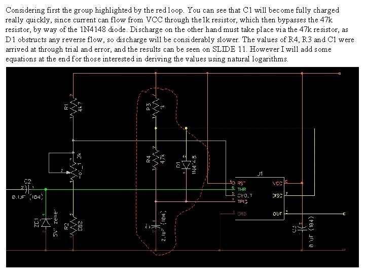
Considering first the group highlighted by the red loop. You can see that C 1 will become fully charged really quickly, since current can flow from VCC through the 1 k resistor, which then bypasses the 47 k resistor, by way of the 1 N 4148 diode. Discharge on the other hand must take place via the 47 k resistor, as D 1 obstructs any reverse flow, so discharge will be considerably slower. The values of R 4, R 3 and C 1 were arrived at through trial and error, and the results can be seen on SLIDE 11. However I will add some equations at the end for those interested in deriving the values using natural logarithms.

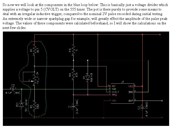
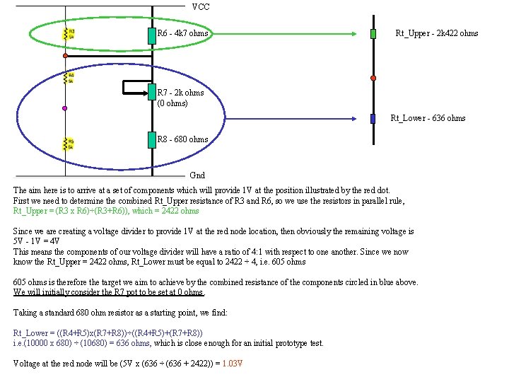
So now we will look at the components in the blue loop below. This is basically just a voltage divider which supplies a voltage to pin 5 (CVOLT) on the 555 timer. The pot is there purely to provide some means to deal with an irregular inductive trigger, compared to the nominal 2 V pulse recorded during initial testing. An extremely wide or narrow sparkplug gap for example, will greatly effect the amplitude of the pulse peak voltage. The values of these components were calculated beforehand, so I will show the calculations on the next few slides.

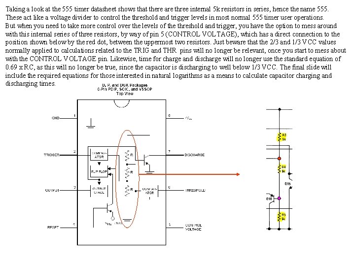
Taking a look at the 555 timer datasheet shows that there are three internal 5 k resistors in series, hence the name 555. These act like a voltage divider to control the threshold and trigger levels in most normal 555 timer user operations. But when you need to take more control over the levels of the threshold and trigger, you have the option to mess around with this internal series of three resistors, by way of pin 5 (CONTROL VOLTAGE), which has a direct connection to the position shown below by the red dot, between the uppermost two resistors. Just beware that the 2/3 and 1/3 VCC values normally applied to calculations related to the TRIG and THR pins will no longer be relevant, once you start to mess about with the CONTROL VOLTAGE pin. Likewise, time for charge and discharge will no longer use the standard equation of 0. 69 x RC, as this will no longer be true, since the capacitor is discharging to well below 1/3 VCC. The final slide will include the required equations for those interested in natural logarithms as a means to calculate capacitor charging and discharging times.

VCC R 6 - 4 k 7 ohms Rt_Upper - 2 k 422 ohms R 7 - 2 k ohms (0 ohms) Rt_Lower - 636 ohms R 8 - 680 ohms Gnd The aim here is to arrive at a set of components which will provide 1 V at the position illustrated by the red dot. First we need to determine the combined Rt_Upper resistance of R 3 and R 6, so we use the resistors in parallel rule, Rt_Upper = (R 3 x R 6)÷(R 3+R 6)), which = 2422 ohms Since we are creating a voltage divider to provide 1 V at the red node location, then obviously the remaining voltage is 5 V - 1 V = 4 V This means the components of our voltage divider will have a ratio of 4: 1 with respect to one another. Since we now know the Rt_Upper = 2422 ohms, Rt_Lower must be equal to 2422 ÷ 4, i. e. 605 ohms is therefore the target we aim to achieve by the combined resistance of the components circled in blue above. We will initially consider the R 7 pot to be set at 0 ohms. Taking a standard 680 ohm resistor as a starting point, we find: Rt_Lower = ((R 4+R 5)x(R 7+R 8))÷((R 4+R 5)+(R 7+R 8)) i. e. (10000 x 680) ÷ (10680) = 636 ohms, which is close enough for an initial prototype test. Voltage at the red node will be (5 V x (636 ÷ (636 + 2422)) = 1. 03 V

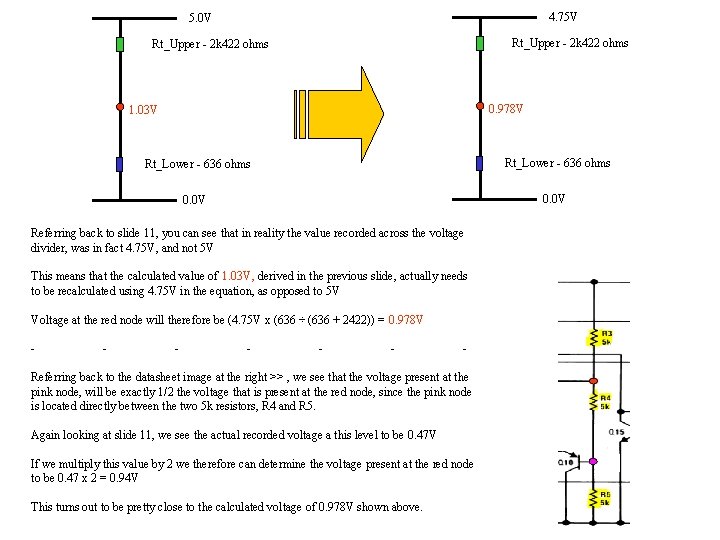
4. 75 V 5. 0 V Rt_Upper - 2 k 422 ohms 0. 978 V 1. 03 V Rt_Lower - 636 ohms 0. 0 V Referring back to slide 11, you can see that in reality the value recorded across the voltage divider, was in fact 4. 75 V, and not 5 V This means that the calculated value of 1. 03 V, derived in the previous slide, actually needs to be recalculated using 4. 75 V in the equation, as opposed to 5 V Voltage at the red node will therefore be (4. 75 V x (636 ÷ (636 + 2422)) = 0. 978 V - - - - Referring back to the datasheet image at the right >> , we see that the voltage present at the pink node, will be exactly 1/2 the voltage that is present at the red node, since the pink node is located directly between the two 5 k resistors, R 4 and R 5. Again looking at slide 11, we see the actual recorded voltage a this level to be 0. 47 V If we multiply this value by 2 we therefore can determine the voltage present at the red node to be 0. 47 x 2 = 0. 94 V This turns out to be pretty close to the calculated voltage of 0. 978 V shown above.

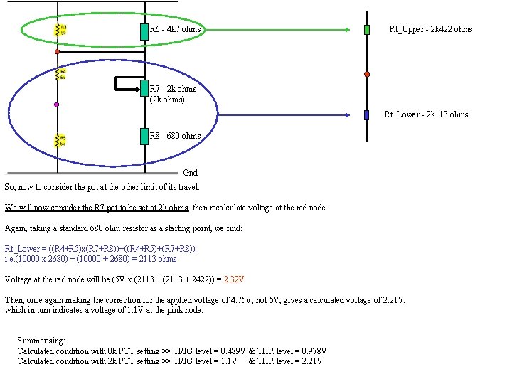
R 6 - 4 k 7 ohms Rt_Upper - 2 k 422 ohms R 7 - 2 k ohms (2 k ohms) Rt_Lower - 2 k 113 ohms R 8 - 680 ohms Gnd So, now to consider the pot at the other limit of its travel. We will now consider the R 7 pot to be set at 2 k ohms. then recalculate voltage at the red node Again, taking a standard 680 ohm resistor as a starting point, we find: Rt_Lower = ((R 4+R 5)x(R 7+R 8))÷((R 4+R 5)+(R 7+R 8)) i. e. (10000 x 2680) ÷ (10000 + 2680) = 2113 ohms. Voltage at the red node will be (5 V x (2113 ÷ (2113 + 2422)) = 2. 32 V Then, once again making the correction for the applied voltage of 4. 75 V, not 5 V, gives a calculated voltage of 2. 21 V, which in turn indicates a voltage of 1. 1 V at the pink node. Summarising: Calculated condition with 0 k POT setting >> TRIG level = 0. 489 V & THR level = 0. 978 V Calculated condition with 2 k POT setting >> TRIG level = 1. 1 V & THR level = 2. 21 V