5 Zerodimensional systems Contents Types of QDs Metal

- Slides: 43

5. Zero-dimensional systems

• Contents • Types of QD’s • Metal clusters. Electronic properties • Fullerenes • Synthetic nanocrystals. • Self-assembled QD’s. • QD’s produced from heterostructures and lithografic etching • Optical properties • Coulomb blockade and single electron devices • Summary 2

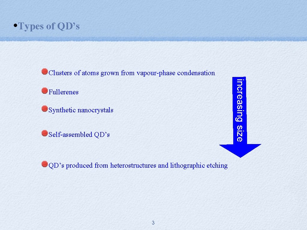
• Types of QD’s Clusters of atoms grown from vapour-phase condensation increasing size Fullerenes Synthetic nanocrystals Self-assembled QD’s produced from heterostructures and lithographic etching 3

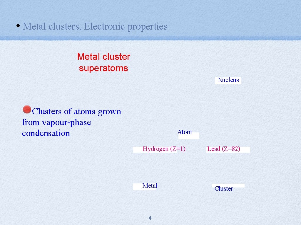
• Metal clusters. Electronic properties Metal cluster superatoms Nucleus Clusters of atoms grown from vapour-phase condensation Atom Hydrogen (Z=1) Metal 4 Lead (Z=82) Cluster

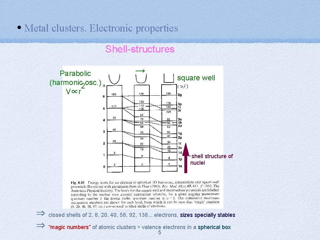
• Metal clusters. Electronic properties Shell-structures Parabolic (harmonic 2 osc. ) V∝r → square well ∼shell structure of nuclei ⇒ closed shells of 2, 8, 20, 40, 58, 92, 138. . . electrons, sizes specially stables ⇒ “magic numbers” of atomic clusters ≅ valence electrons in a spherical box 5

• Metal clusters. Electronic properties Electron spill-out Jellium (sphere) model 6

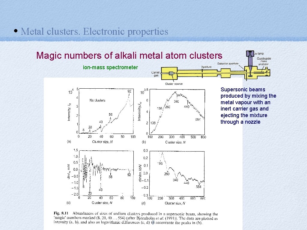
• Metal clusters. Electronic properties Magic numbers of alkali metal atom clusters ion-mass spectrometer Supersonic beams produced by mixing the metal vapour with an inert carrier gas and ejecting the mixture through a nozzle Fig 8. 11 7

• Metal clusters. Electronic properties Spherical shell closing → N=1430 atoms complete icosahedral clusters (e. g. Al ) → 13 N=25000 atoms. . . → bulk material 8

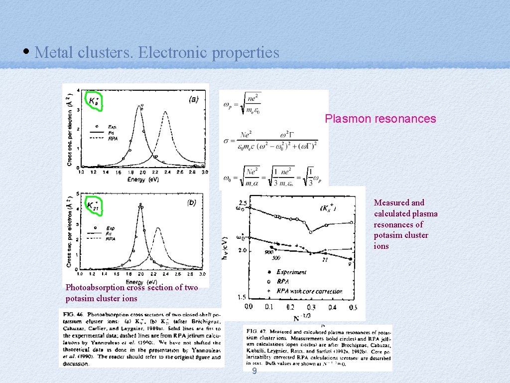
• Metal clusters. Electronic properties Plasmon resonances Measured and calculated plasma resonances of potasim cluster ions Photoabsorption cross section of two potasim cluster ions 9

• Fullerenes (next chapter) C 60 10

• Synthetic nanocrystals. • Obtained by chemical methods. • Precipitates in colloids. • Nanocrystals in insulating matrix, e. g. , Cd. Se in glassy matrix, Cu. Cl in Na. Cl crystals, Si, Ge. . . • Size control (~1 nm-> ~200 nm) 11

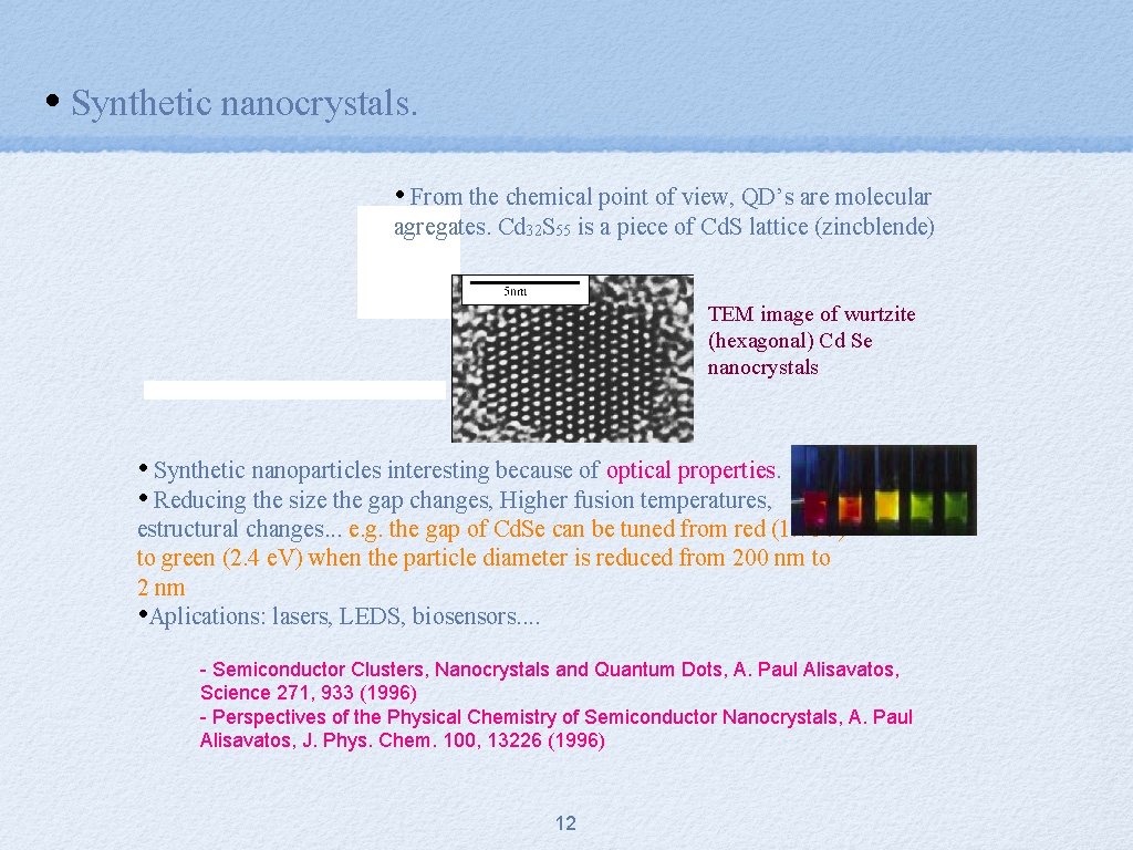
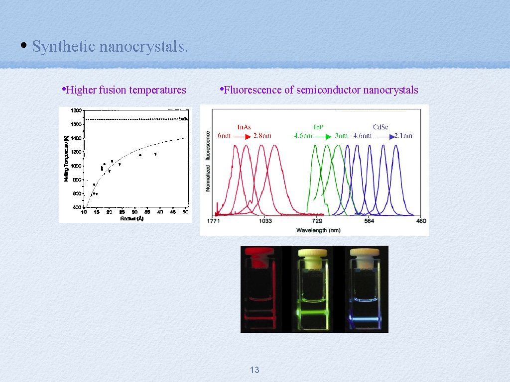
• Synthetic nanocrystals. • From the chemical point of view, QD’s are molecular agregates. Cd 32 S 55 is a piece of Cd. S lattice (zincblende) TEM image of wurtzite (hexagonal) Cd Se nanocrystals • Synthetic nanoparticles interesting because of optical properties. • Reducing the size the gap changes, Higher fusion temperatures, estructural changes. . . e. g. the gap of Cd. Se can be tuned from red (1. 7 e. V) to green (2. 4 e. V) when the particle diameter is reduced from 200 nm to 2 nm • Aplications: lasers, LEDS, biosensors. . - Semiconductor Clusters, Nanocrystals and Quantum Dots, A. Paul Alisavatos, Science 271, 933 (1996) - Perspectives of the Physical Chemistry of Semiconductor Nanocrystals, A. Paul Alisavatos, J. Phys. Chem. 100, 13226 (1996) 12

• Synthetic nanocrystals. • Higher fusion temperatures • Fluorescence of semiconductor nanocrystals 13

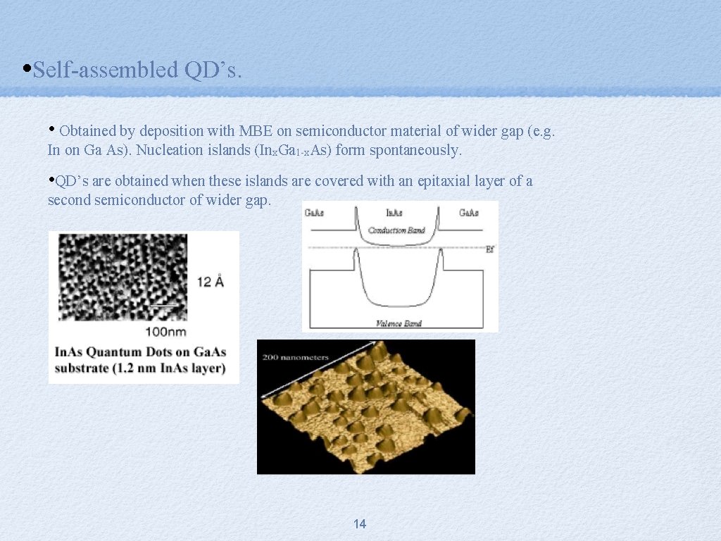
• Self-assembled QD’s. • Obtained by deposition with MBE on semiconductor material of wider gap (e. g. In on Ga As). Nucleation islands (Inx. Ga 1 -x. As) form spontaneously. • QD’s are obtained when these islands are covered with an epitaxial layer of a second semiconductor of wider gap. 14

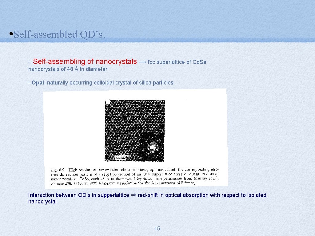
• Self-assembled QD’s. - Self-assembling of nanocrystals → fcc superlattice of Cd. Se nanocrystals of 48 Å in diameter - Opal: naturally occurring colloidal crystal of silica particles Interaction between QD’s in supperlattice ⇒ red-shift in optical absorption with respect to isolated nanocrystal 15

• Self-assembled QD’s. 16

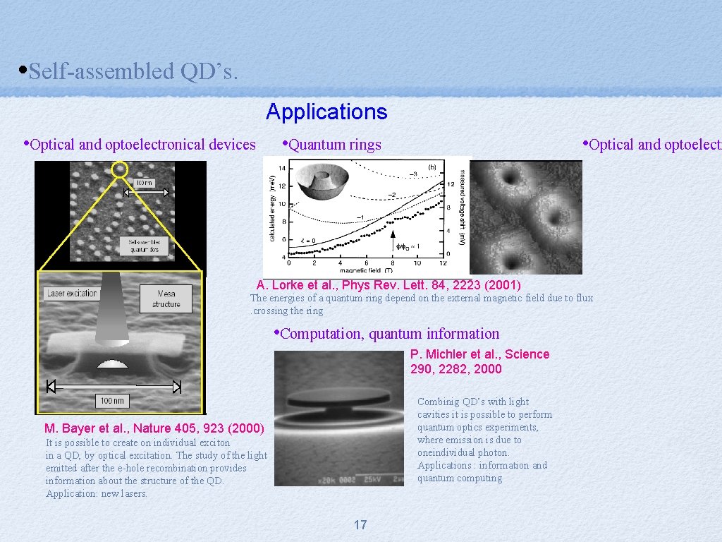
• Self-assembled QD’s. Applications • Optical and optoelectronical devices • Quantum rings • Optical and optoelectr A. Lorke et al. , Phys Rev. Lett. 84, 2223 (2001) The energies of a quantum ring depend on the external magnetic field due to flux. crossing the ring • Computation, quantum information P. Michler et al. , Science 290, 2282, 2000 Combinig QD’s with light cavities it is possible to perform quantum optics experiments, where emission is due to oneindividual photon. Applications : information and quantum computing M. Bayer et al. , Nature 405, 923 (2000) It is possible to create on individual exciton in a QD, by optical excitation. The study of the light emitted after the e-hole recombination provides information about the structure of the QD. Application: new lasers. 17

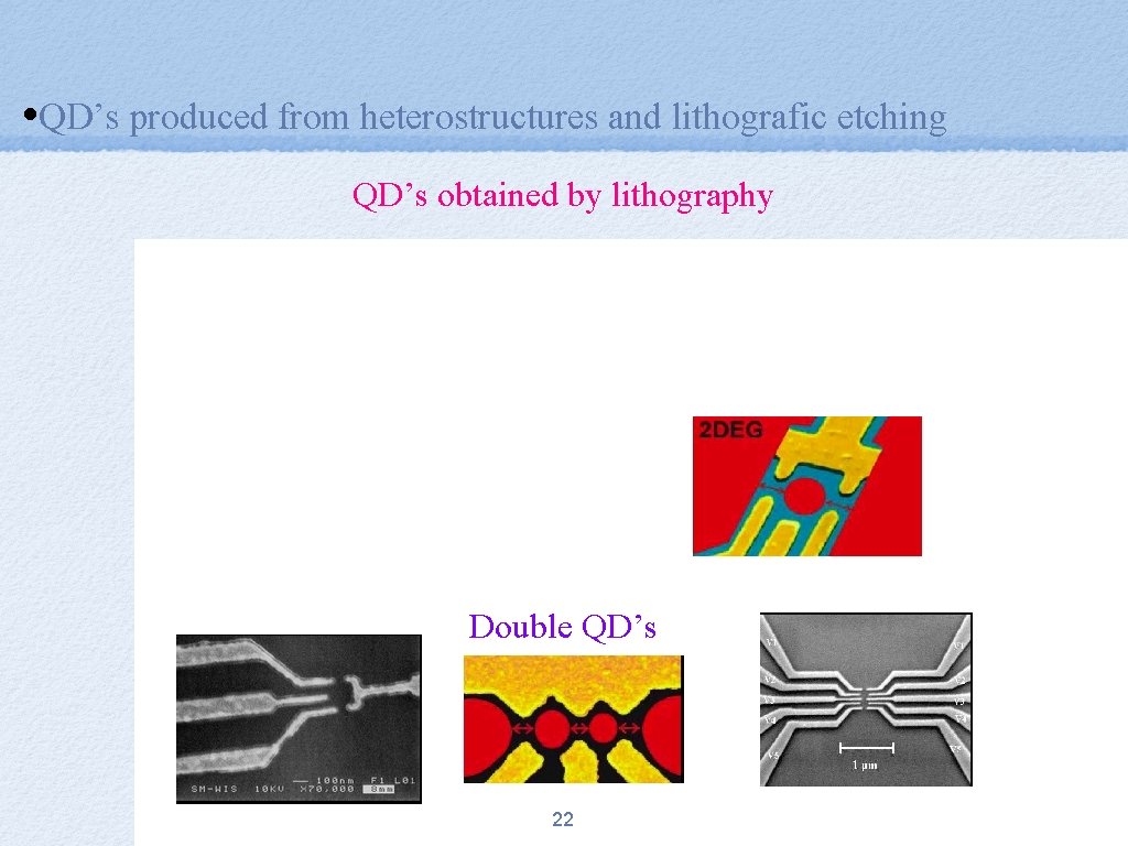
• QD’s produced from heterostructures and lithografic etching Lithographic etching • Obtained from Ga. As/Al. GAAs heterostructures, whre a 2 D electron gas has been formed. • Lateral (in the plane of the 2 D electron gas) QD’s are produced by lithographic etching. • Also vertical QD’s are produced bt MBE growth in the direction perpendicular to the electron confinement plane. Size: 10 -20 nm to μm’s Reed et al. , PRL 60, 535 (1988) 18

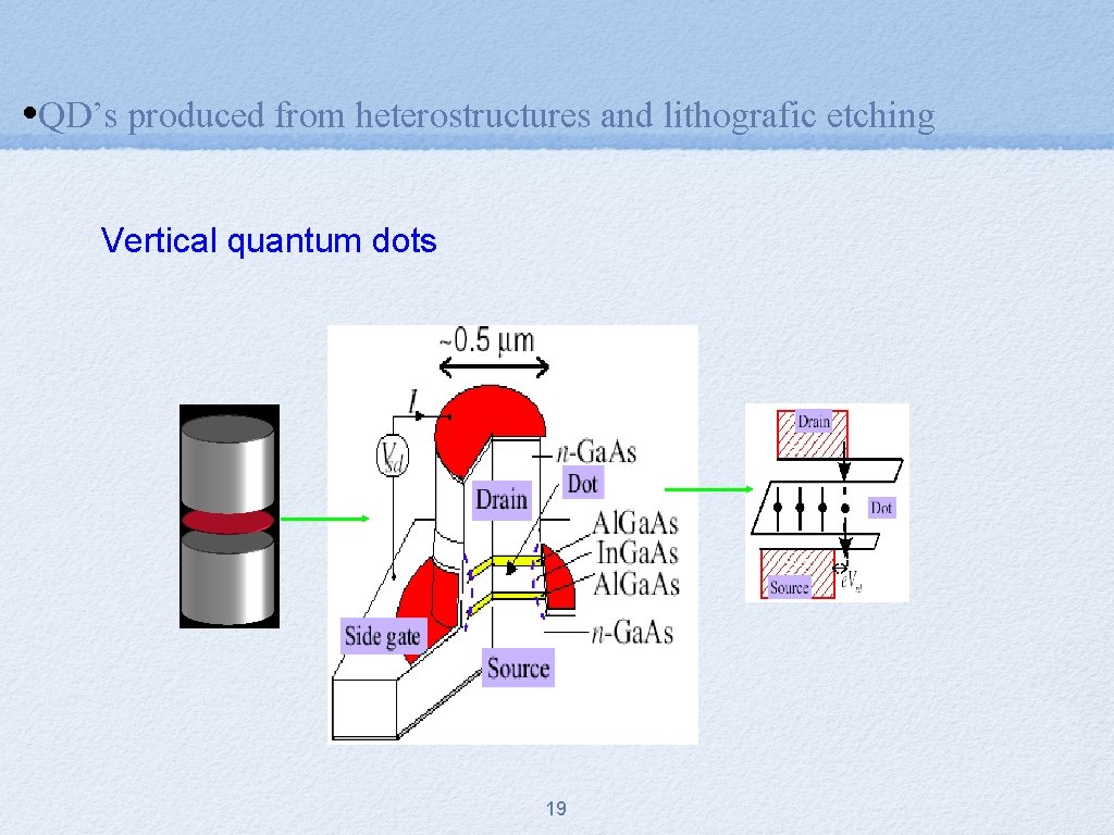
• QD’s produced from heterostructures and lithografic etching Vertical quantum dots 19

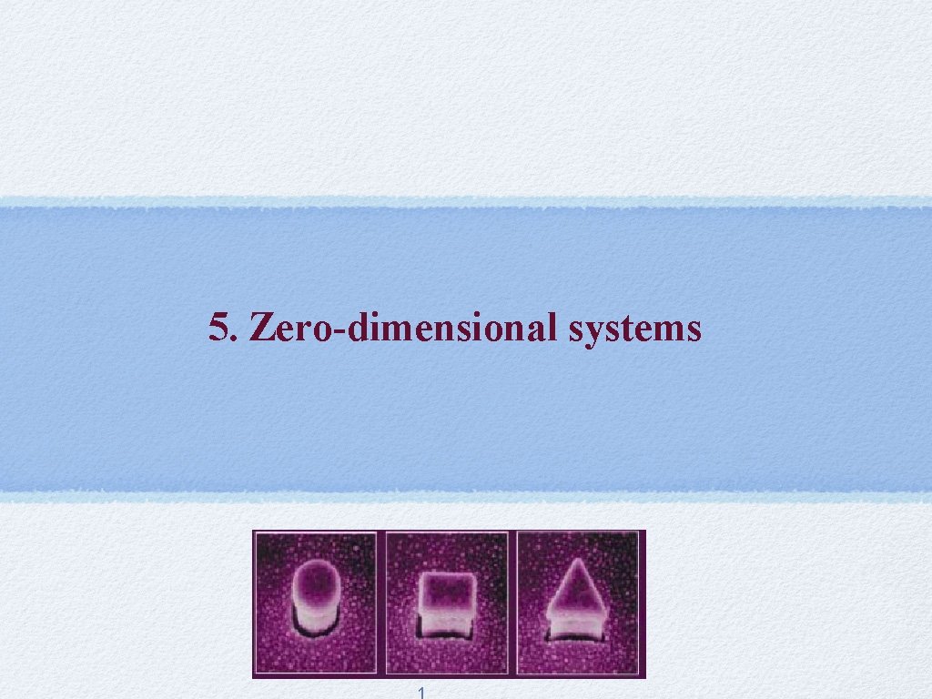
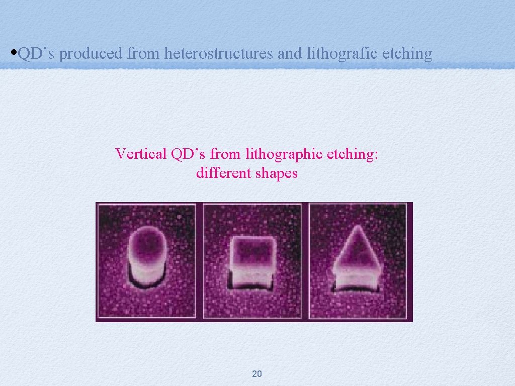
• QD’s produced from heterostructures and lithografic etching Vertical QD’s from lithographic etching: different shapes 20

• QD’s produced from heterostructures and lithografic etching 21

• QD’s produced from heterostructures and lithografic etching QD’s obtained by lithography Double QD’s 22

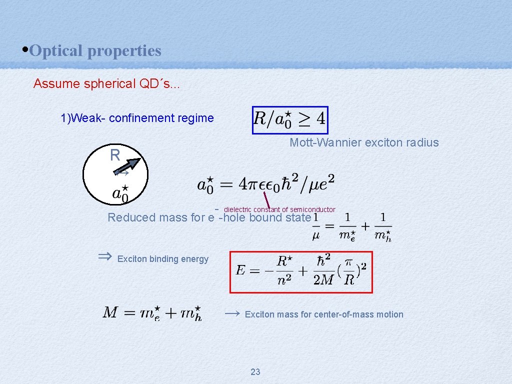
• Optical properties Assume spherical QD´s. . . 1)Weak- confinement regime Mott-Wannier exciton radius R ↔ - dielectric constant of semiconductor Reduced mass for e -hole bound state ⇒ Exciton binding energy → Exciton mass for center-of-mass motion 23

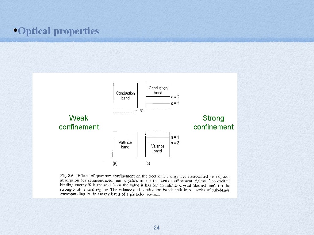
• Optical properties Weak confinement Strong confinement 24

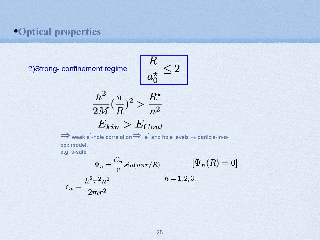
• Optical properties 2)Strong- confinement regime - ⇒ weak e -hole correlation⇒ e - and hole levels → particle-in-a- box model: e. g. s-sate 25

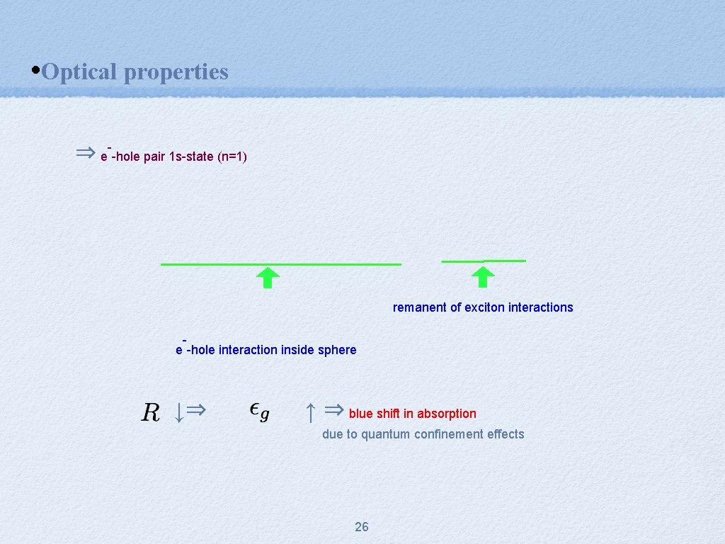
• Optical properties ⇒ e--hole pair 1 s-state (n=1) remanent of exciton interactions e -hole interaction inside sphere ↓⇒ ↑ ⇒ blue shift in absorption due to quantum confinement effects 26

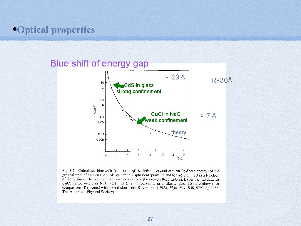
• Optical properties Blue shift of energy gap ≅ 29Å Cd. S in glass strong confinement Cu. Cl in Na. Cl weak confinement theory 27 R≅30Å ≅ 7Å

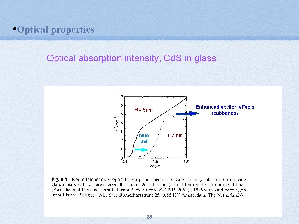
• Optical properties Optical absorption intensity, Cd. S in glass Enhanced exciton effects (subbands) R= 5 nm blue shift 28 1. 7 nm

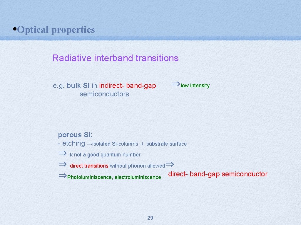
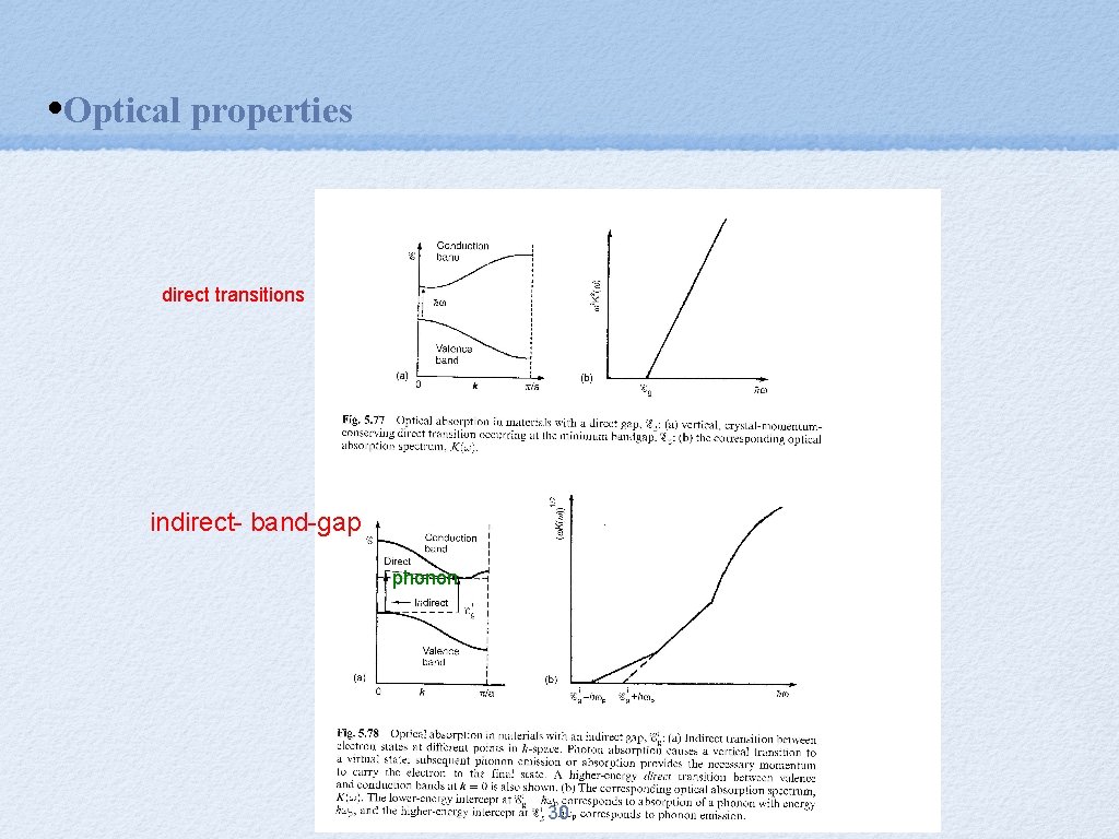
• Optical properties Radiative interband transitions e. g. bulk Si in indirect- band-gap semiconductors ⇒low intensity porous Si: - etching →isolated Si-columns ⊥ substrate surface ⇒ k not a good quantum number ⇒ direct transitions without phonon allowed⇒ ⇒Photoluminiscence, electroluminiscence direct- band-gap semiconductor 29

• Optical properties direct transitions indirect- band-gap phonon 30

• Coulomb blockade and single electron devices Coulomb blockade Single electron transistors (SET´s) Electron non-coherent tunnelling Diferencial conductance vs. V gate ⇒ Peaks corresponding to one electron addition ⇒ Coulomb blockade model 31

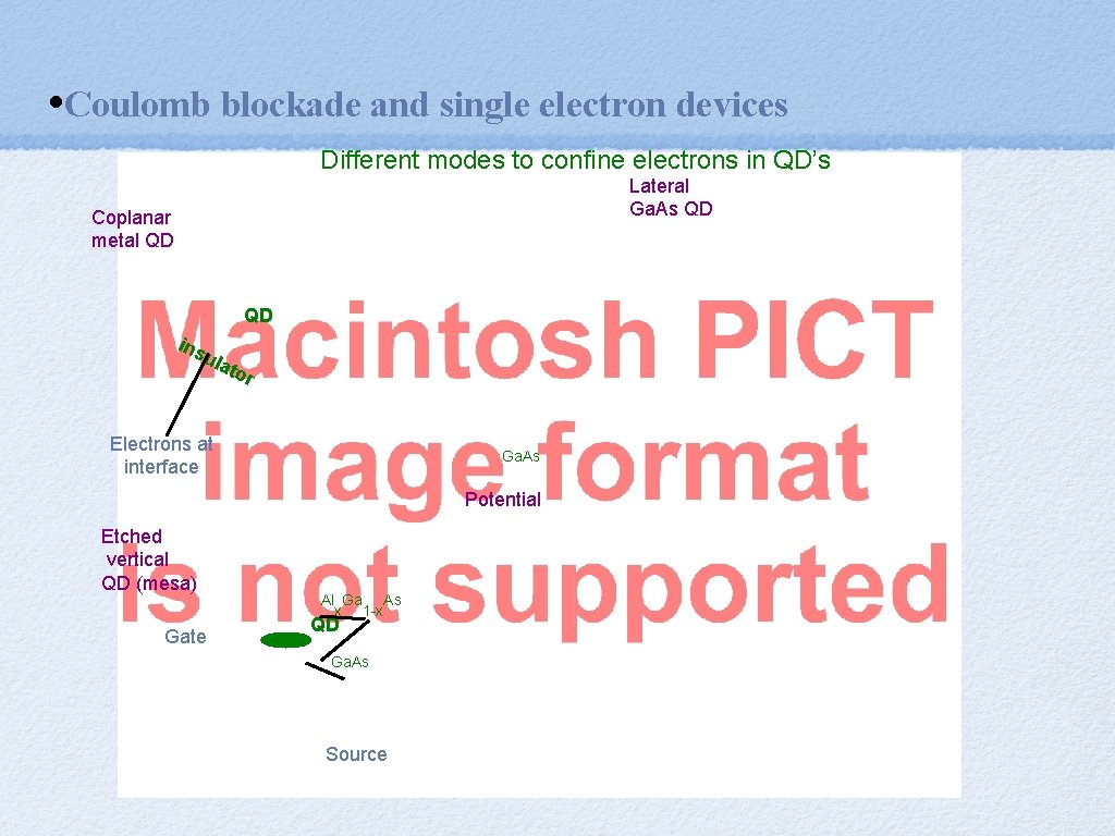
• Coulomb blockade and single electron devices Different modes to confine electrons in QD’s Lateral Ga. As QD Coplanar metal QD QD ins ula tor Electrons at interface Ga. As Potential Etched vertical QD (mesa) Gate Al Ga As x 1 -x QD Ga. As Source

• Coulomb blockade and single electron devices Differencial conductance vs. gate voltage

• Coulomb blockade and single electron devices Coulomb blockade model 2 Adding 1 e- ⇒ΔE=e /2 C , C=capacity between dot and surrounding threshold energy above E for current flow F - 2 If k T < e /2 C ⇒ no current B , Coulomb blockade only evident at very low T

• Coulomb blockade and single electron devices But a current can be made to flow varying Vg voltage 2 E=QV + Q /2 C g → parabola with min. at Q =-CV 0 g , but charge is quantized Q=Ne 7 metallic QD’s, ∼ 10 electrons, extra charge on surface → Q /2 C ∼ exact ∼ 2 exact for Approximative for semiconductor QD’s, N ∼< 50 electrons, confinement of electron wave function → espatial size quantization → discrete energy spectrum 35

• Coulomb blockade and single electron devices V =Ne/C g V =(N+1/2)e/C g E(N+1)-E(N)= 2 e /2 C E(N+1)=E(N) electron-hole tunneling 2 gap e /C 36 2 E=QV + Q /2 C g

• Coulomb blockade and single electron devices - - Electron transport controlled e by e ↔ single electron transistor 37

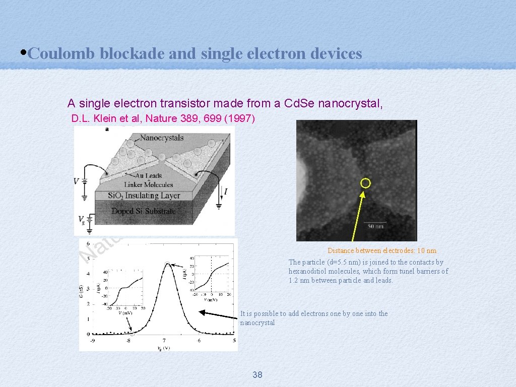
• Coulomb blockade and single electron devices A single electron transistor made from a Cd. Se nanocrystal, D. L. Klein et al, Nature 389, 699 (1997) Distance between electrodes: 10 nm The particle (d=5. 5 nm) is joined to the contacts by hexanoditiol molecules, which form tunel barriers of 1. 2 nm between particle and leads. It is possible to add electrons one by one into the nanocrystal 38

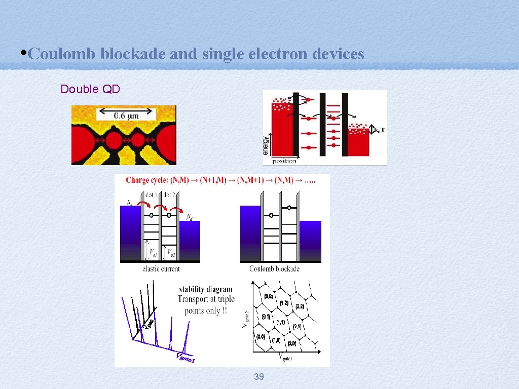
• Coulomb blockade and single electron devices Double QD 39

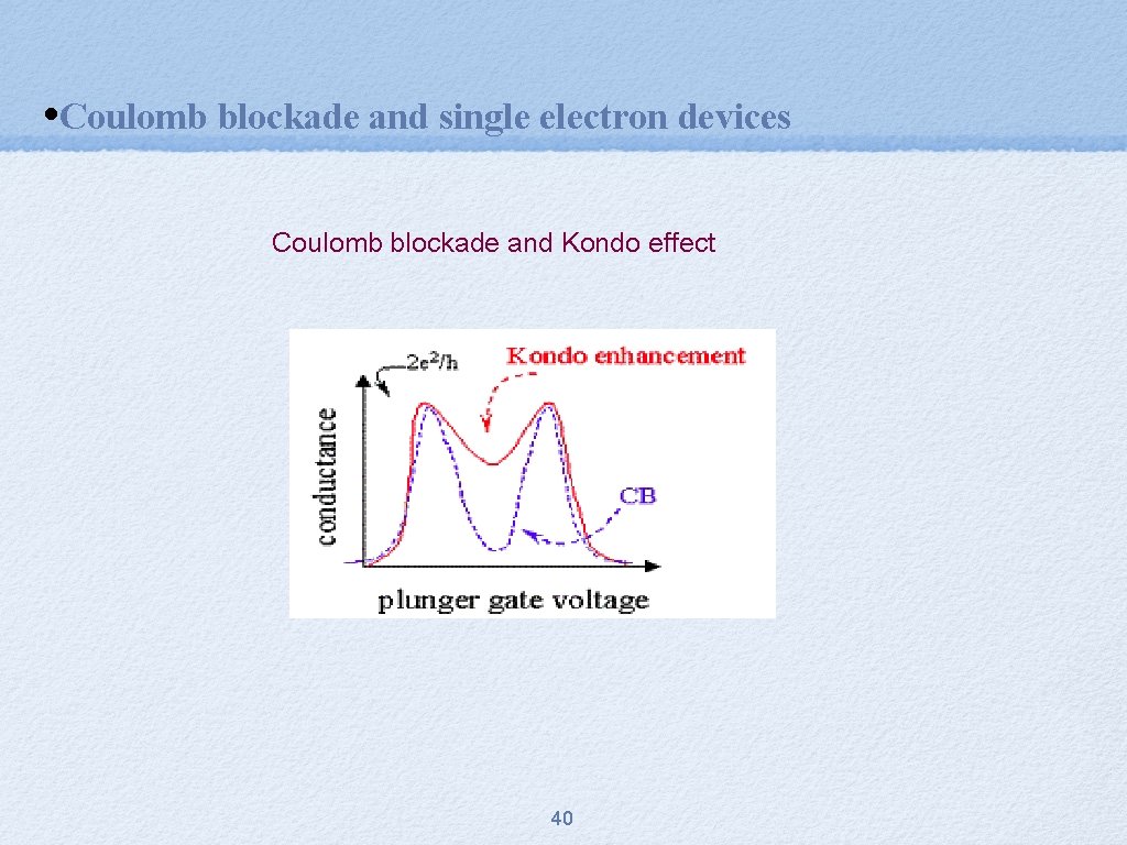
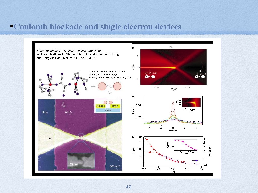
• Coulomb blockade and single electron devices Coulomb blockade and Kondo effect 40

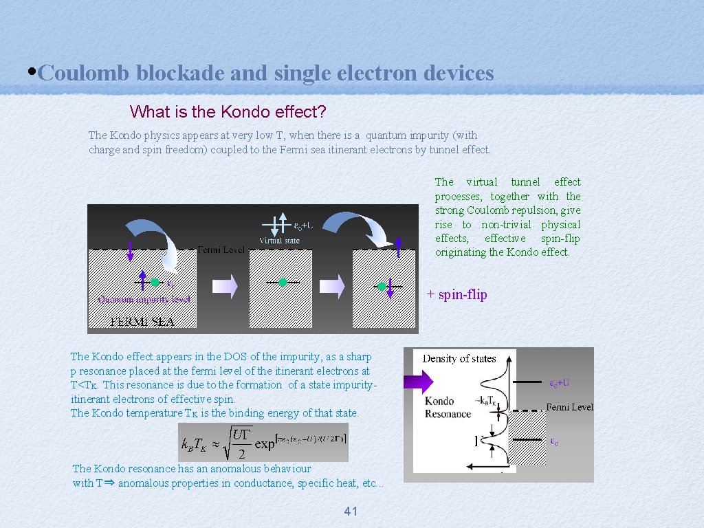
• Coulomb blockade and single electron devices What is the Kondo effect? The Kondo physics appears at very low T, when there is a quantum impurity (with charge and spin freedom) coupled to the Fermi sea itinerant electrons by tunnel effect. The virtual tunnel effect processes, together with the strong Coulomb repulsion, give rise to non-trivial physical effects, effective spin-flip originating the Kondo effect. + spin-flip The Kondo effect appears in the DOS of the impurity, as a sharp p resonance placed at the fermi level of the itinerant electrons at T<TK. This resonance is due to the formation of a state impurityitinerant electrons of effective spin. The Kondo temperature TK is the binding energy of that state. The Kondo resonance has an anomalous behaviour with T⇒ anomalous properties in conductance, specific heat, etc. . . 41

• Coulomb blockade and single electron devices 42

• Summary • We have described the characteristics and most important properties of different systems with confinement in the three dimensions of space, called quantum dots or artificial atoms. • For metal clusters we have described the main properties of their electronic structure: the shell structure and the magic numbers in the sizes of metal atom clusters. • We have described the methods of producing nanocrystals and their important optical properties, dependent on their size. • We have studied briefly the methods to obtain self-assembled QD’s and their main interests. • We have studied the optical properties of quantum dots, attending to the confinement regime. • Finally we have addressed the problem of electron transport through a QD between two leads and we have studied the Coulomb blockade model. 43