5 Steps of MIPS Datapath Figure A 2
![Inst. Set Processor Controller IR <= mem[PC]; PC <= PC + 4 JSR A Inst. Set Processor Controller IR <= mem[PC]; PC <= PC + 4 JSR A](https://slidetodoc.com/presentation_image_h2/179459b1a3276ebc9eae5451ecab73d2/image-3.jpg)
- Slides: 25

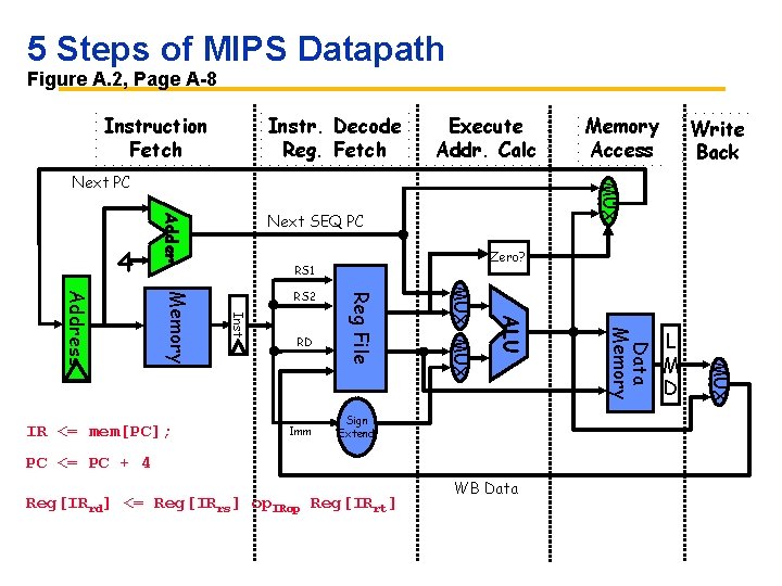
5 Steps of MIPS Datapath Figure A. 2, Page A-8 Instruction Fetch Instr. Decode Reg. Fetch Execute Addr. Calc Next SEQ PC Adder 4 PC <= PC + 4 Reg[IRrd] <= Reg[IRrs] op. IRop Reg[IRrt] WB Data L M D MUX Sign Extend Data Memory ALU Imm MUX RD Reg File Inst Memory Address IR <= mem[PC]; Zero? RS 1 RS 2 Write Back MUX Next PC Memory Access

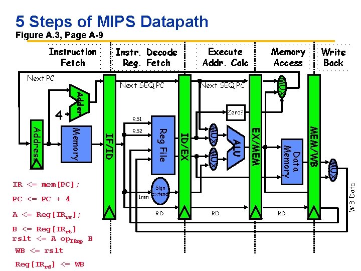
5 Steps of MIPS Datapath Figure A. 3, Page A-9 Execute Addr. Calc Instr. Decode Reg. Fetch Next SEQ PC Adder 4 Zero? RS 1 RD RD RD MUX Sign Extend MEM/WB Data Memory Reg[IRrd] <= WB EX/MEM B <= Reg[IRrt] rslt <= A op. IRop B WB <= rslt ALU A <= Reg[IRrs]; Imm MUX PC <= PC + 4 ID/EX IR <= mem[PC]; Reg File IF/ID Memory Address RS 2 Write Back MUX Next PC Memory Access WB Data Instruction Fetch
![Inst Set Processor Controller IR memPC PC PC 4 JSR A Inst. Set Processor Controller IR <= mem[PC]; PC <= PC + 4 JSR A](https://slidetodoc.com/presentation_image_h2/179459b1a3276ebc9eae5451ecab73d2/image-3.jpg)
Inst. Set Processor Controller IR <= mem[PC]; PC <= PC + 4 JSR A <= Reg[IRrs]; JR br if bop(A, b) Ifetch op. Fetch-DCD ST B <= Reg[IRrt] jmp RR PC <= IRjaddr r <= A op. IRop B RI LD r <= A op. IRop IRim r <= A + IRim WB <= r WB <= Mem[r] PC <= PC+IRim WB <= r Reg[IRrd] <= WB

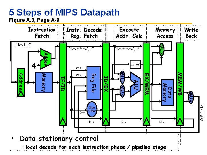
5 Steps of MIPS Datapath Figure A. 3, Page A-9 Execute Addr. Calc Instr. Decode Reg. Fetch Next SEQ PC Adder 4 Zero? RS 1 RD • Data stationary control RD RD – local decode for each instruction phase / pipeline stage MUX Sign Extend MEM/WB Data Memory EX/MEM ALU MUX ID/EX Imm Reg File IF/ID Memory Address RS 2 Write Back MUX Next PC Memory Access WB Data Instruction Fetch

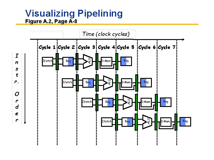
Visualizing Pipelining Figure A. 2, Page A-8 Time (clock cycles) Reg DMem Ifetch Reg DMem Reg ALU O r d e r Ifetch ALU I n s t r. ALU Cycle 1 Cycle 2 Cycle 3 Cycle 4 Cycle 5 Cycle 6 Cycle 7 Ifetch Reg Reg DMem Reg

Pipelining is not quite that easy! • Limits to pipelining: Hazards prevent next instruction from executing during its designated clock cycle – Structural hazards: HW cannot support this combination of instructions (single person to fold and put clothes away) – Data hazards: Instruction depends on result of prior instruction still in the pipeline (missing sock) – Control hazards: Caused by delay between the fetching of instructions and decisions about changes in control flow (branches and jumps).

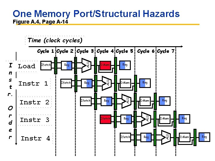
One Memory Port/Structural Hazards Figure A. 4, Page A-14 Time (clock cycles) Instr 2 Instr 3 Instr 4 DMem Ifetch Reg DMem Reg ALU Instr 1 Reg ALU Ifetch ALU O r d e r Load ALU I n s t r. ALU Cycle 1 Cycle 2 Cycle 3 Cycle 4 Cycle 5 Cycle 6 Cycle 7 Ifetch Reg Reg DMem Reg

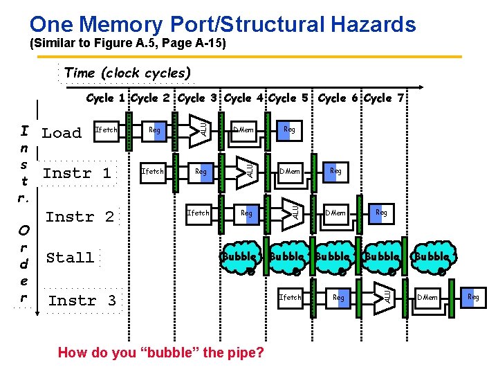
One Memory Port/Structural Hazards (Similar to Figure A. 5, Page A-15) Time (clock cycles) Instr 1 Instr 2 Stall Reg DMem Ifetch Reg DMem Reg ALU Ifetch Bubble Instr 3 How do you “bubble” the pipe? Reg DMem Bubble Ifetch Reg Bubble ALU O r d e r Load ALU I n s t r. ALU Cycle 1 Cycle 2 Cycle 3 Cycle 4 Cycle 5 Cycle 6 Cycle 7 Bubble DMem Reg

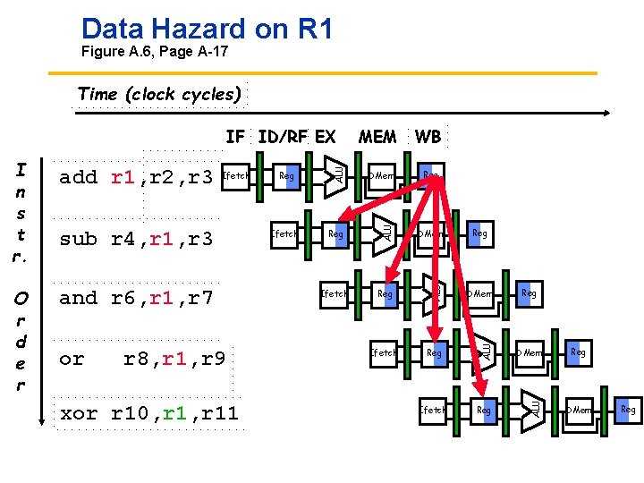
Data Hazard on R 1 Figure A. 6, Page A-17 Time (clock cycles) and r 6, r 1, r 7 or r 8, r 1, r 9 xor r 10, r 11 Ifetch Reg DMem Ifetch Reg ALU sub r 4, r 1, r 3 Reg ALU Ifetch ALU O r d e r add r 1, r 2, r 3 WB ALU I n s t r. MEM ALU IF ID/RF EX Reg Reg DMem Reg

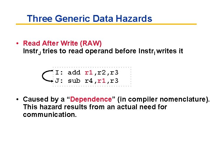
Three Generic Data Hazards • Read After Write (RAW) Instr. J tries to read operand before Instr. I writes it I: add r 1, r 2, r 3 J: sub r 4, r 1, r 3 • Caused by a “Dependence” (in compiler nomenclature). This hazard results from an actual need for communication.

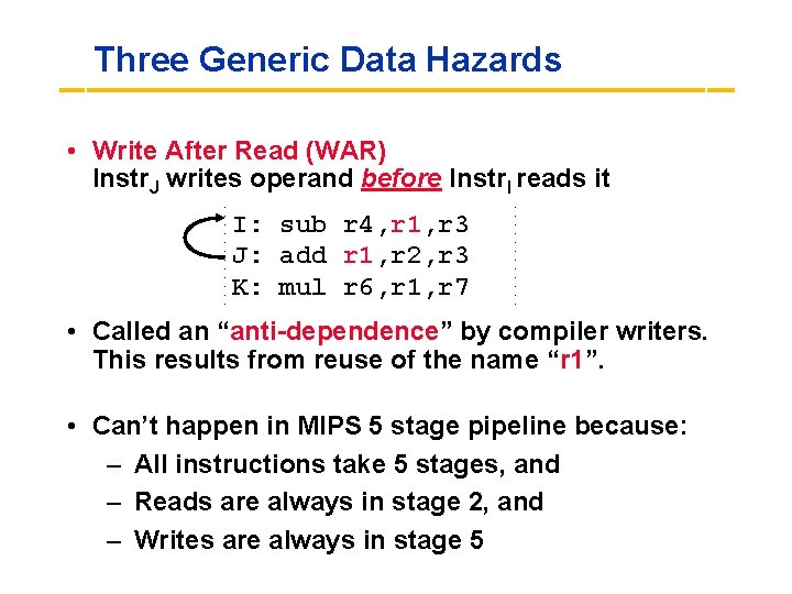
Three Generic Data Hazards • Write After Read (WAR) Instr. J writes operand before Instr. I reads it I: sub r 4, r 1, r 3 J: add r 1, r 2, r 3 K: mul r 6, r 1, r 7 • Called an “anti-dependence” by compiler writers. This results from reuse of the name “r 1”. • Can’t happen in MIPS 5 stage pipeline because: – All instructions take 5 stages, and – Reads are always in stage 2, and – Writes are always in stage 5

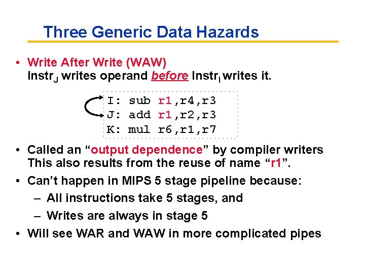
Three Generic Data Hazards • Write After Write (WAW) Instr. J writes operand before Instr. I writes it. I: sub r 1, r 4, r 3 J: add r 1, r 2, r 3 K: mul r 6, r 1, r 7 • Called an “output dependence” by compiler writers This also results from the reuse of name “r 1”. • Can’t happen in MIPS 5 stage pipeline because: – All instructions take 5 stages, and – Writes are always in stage 5 • Will see WAR and WAW in more complicated pipes

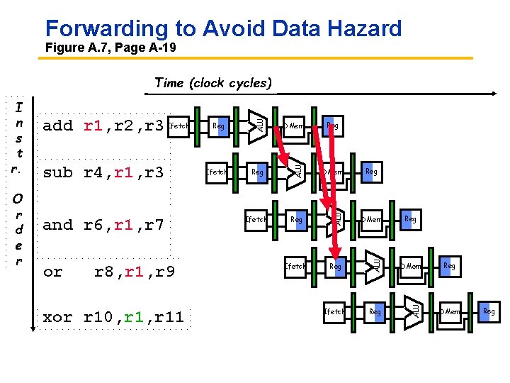
Forwarding to Avoid Data Hazard Figure A. 7, Page A-19 or r 8, r 1, r 9 xor r 10, r 11 Reg DMem Ifetch Reg ALU and r 6, r 1, r 7 Ifetch DMem ALU sub r 4, r 1, r 3 Reg ALU O r d e r add r 1, r 2, r 3 Ifetch ALU I n s t r. ALU Time (clock cycles) Reg Reg DMem Reg

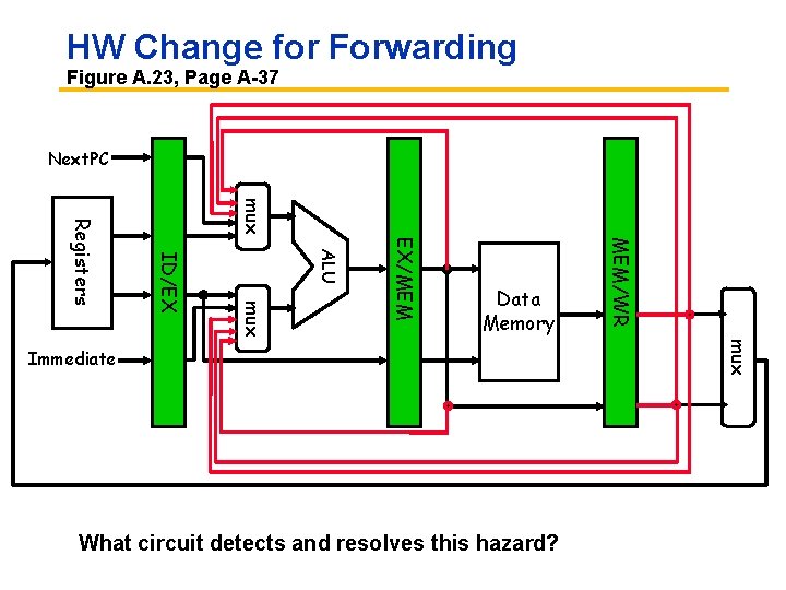
HW Change for Forwarding Figure A. 23, Page A-37 Next. PC mux What circuit detects and resolves this hazard? mux Immediate MEM/WR EX/MEM ALU mux ID/EX Registers Data Memory

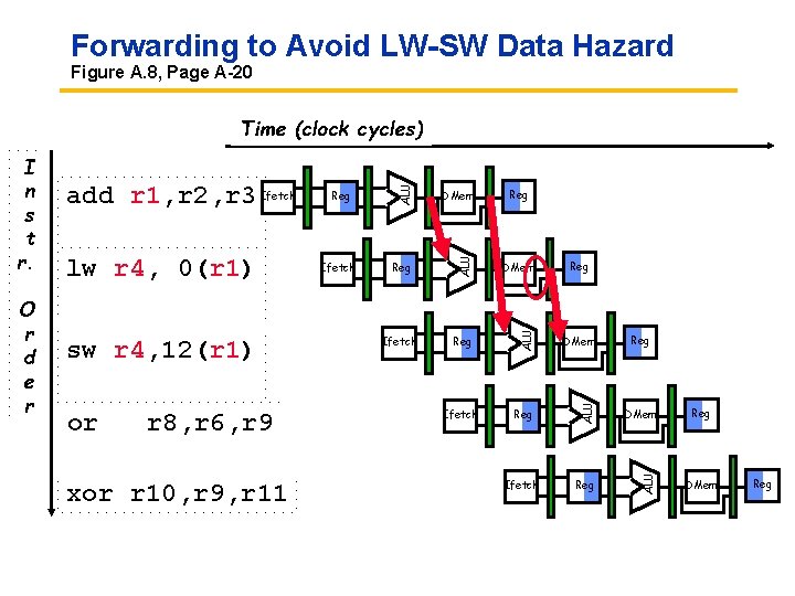
Forwarding to Avoid LW-SW Data Hazard Figure A. 8, Page A-20 or r 8, r 6, r 9 xor r 10, r 9, r 11 Reg DMem Ifetch Reg ALU sw r 4, 12(r 1) Ifetch DMem ALU lw r 4, 0(r 1) Reg ALU O r d e r add r 1, r 2, r 3 Ifetch ALU I n s t r. ALU Time (clock cycles) Reg Reg DMem Reg

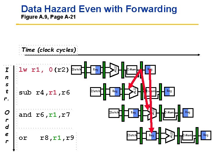
Data Hazard Even with Forwarding Figure A. 9, Page A-21 and r 6, r 1, r 7 or r 8, r 1, r 9 DMem Ifetch Reg DMem Reg Ifetch Reg Reg DMem ALU O r d e r sub r 4, r 1, r 6 Reg ALU lw r 1, 0(r 2) Ifetch ALU I n s t r. ALU Time (clock cycles) Reg DMem Reg

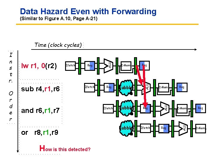
Data Hazard Even with Forwarding (Similar to Figure A. 10, Page A-21) Reg DMem Ifetch Reg Bubble Ifetch Bubble Reg Bubble Ifetch and r 6, r 1, r 7 or r 8, r 1, r 9 How is this detected? Reg DMem ALU sub r 4, r 1, r 6 Ifetch ALU O r d e r lw r 1, 0(r 2) ALU I n s t r. ALU Time (clock cycles) Reg DMem

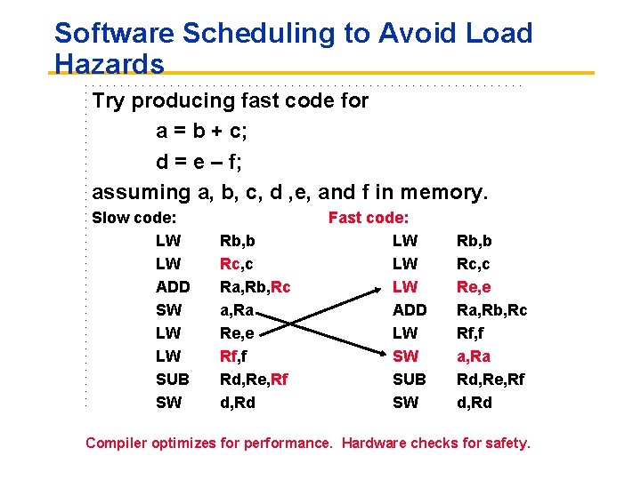
Software Scheduling to Avoid Load Hazards Try producing fast code for a = b + c; d = e – f; assuming a, b, c, d , e, and f in memory. Slow code: LW LW ADD SW LW LW SUB SW Rb, b Rc, c Ra, Rb, Rc a, Ra Re, e Rf, f Rd, Re, Rf d, Rd Fast code: LW LW LW ADD LW SW SUB SW Rb, b Rc, c Re, e Ra, Rb, Rc Rf, f a, Ra Rd, Re, Rf d, Rd Compiler optimizes for performance. Hardware checks for safety.

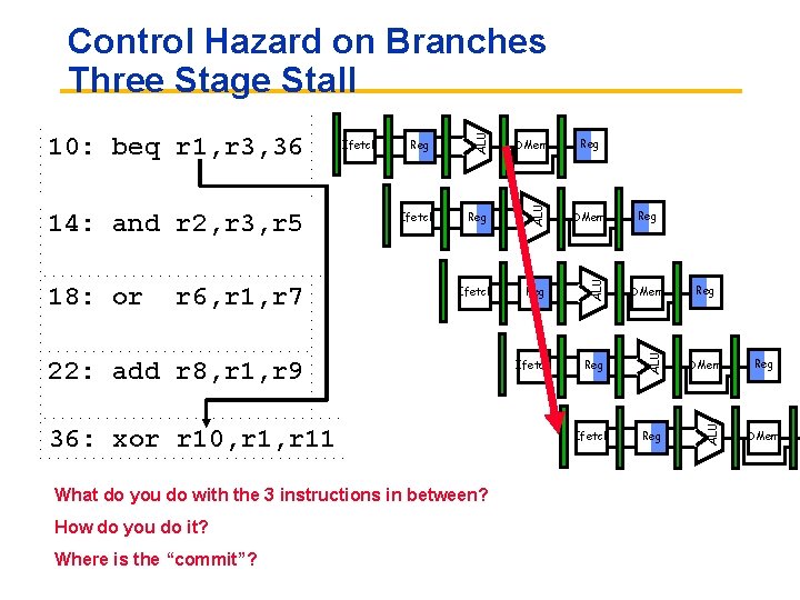
Reg DMem Ifetch Reg ALU r 6, r 1, r 7 Ifetch DMem ALU 18: or Reg ALU 14: and r 2, r 3, r 5 Ifetch ALU 10: beq r 1, r 3, 36 ALU Control Hazard on Branches Three Stage Stall 22: add r 8, r 1, r 9 36: xor r 10, r 11 What do you do with the 3 instructions in between? How do you do it? Where is the “commit”? Reg Reg DMem

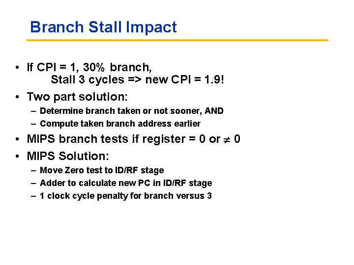
Branch Stall Impact • If CPI = 1, 30% branch, Stall 3 cycles => new CPI = 1. 9! • Two part solution: – Determine branch taken or not sooner, AND – Compute taken branch address earlier • MIPS branch tests if register = 0 or 0 • MIPS Solution: – Move Zero test to ID/RF stage – Adder to calculate new PC in ID/RF stage – 1 clock cycle penalty for branch versus 3

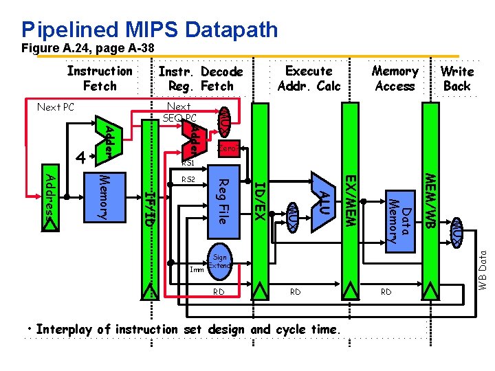
Pipelined MIPS Datapath Figure A. 24, page A-38 Instruction Fetch Memory Access Write Back Adder MUX Next SEQ PC Next PC Zero? RS 1 RD RD • Interplay of instruction set design and cycle time. RD MUX Sign Extend MEM/WB Data Memory EX/MEM ALU MUX ID/EX Imm Reg File IF/ID Memory Address RS 2 WB Data 4 Execute Addr. Calc Instr. Decode Reg. Fetch

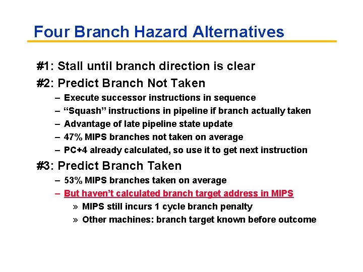
Four Branch Hazard Alternatives #1: Stall until branch direction is clear #2: Predict Branch Not Taken – – – Execute successor instructions in sequence “Squash” instructions in pipeline if branch actually taken Advantage of late pipeline state update 47% MIPS branches not taken on average PC+4 already calculated, so use it to get next instruction #3: Predict Branch Taken – 53% MIPS branches taken on average – But haven’t calculated branch target address in MIPS » MIPS still incurs 1 cycle branch penalty » Other machines: branch target known before outcome

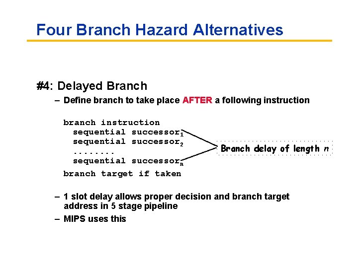
Four Branch Hazard Alternatives #4: Delayed Branch – Define branch to take place AFTER a following instruction branch instruction sequential successor 1 sequential successor 2. . . . sequential successorn branch target if taken Branch delay of length n – 1 slot delay allows proper decision and branch target address in 5 stage pipeline – MIPS uses this

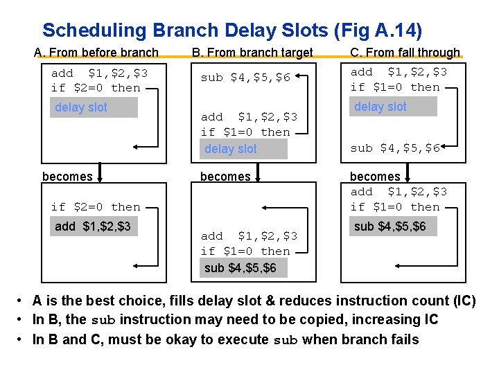
Scheduling Branch Delay Slots (Fig A. 14) A. From before branch add $1, $2, $3 if $2=0 then delay slot becomes B. From branch target sub $4, $5, $6 add $1, $2, $3 if $1=0 then delay slot becomes if $2=0 then add $1, $2, $3 if $1=0 then sub $4, $5, $6 C. From fall through add $1, $2, $3 if $1=0 then delay slot sub $4, $5, $6 becomes add $1, $2, $3 if $1=0 then sub $4, $5, $6 • A is the best choice, fills delay slot & reduces instruction count (IC) • In B, the sub instruction may need to be copied, increasing IC • In B and C, must be okay to execute sub when branch fails

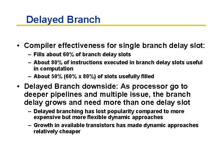
Delayed Branch • Compiler effectiveness for single branch delay slot: – Fills about 60% of branch delay slots – About 80% of instructions executed in branch delay slots useful in computation – About 50% (60% x 80%) of slots usefully filled • Delayed Branch downside: As processor go to deeper pipelines and multiple issue, the branch delay grows and need more than one delay slot – Delayed branching has lost popularity compared to more expensive but more flexible dynamic approaches – Growth in available transistors has made dynamic approaches relatively cheaper