40 nm Stratix IV FPGAs Innovation Without Compromise
- Slides: 12

40 -nm Stratix IV FPGAs Innovation Without Compromise © 2008 Altera Corporation—Public

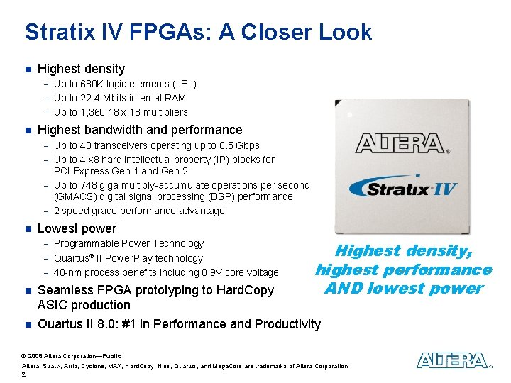
Stratix IV FPGAs: A Closer Look n Highest density - Up to 680 K logic elements (LEs) - Up to 22. 4 -Mbits internal RAM - Up to 1, 360 18 x 18 multipliers n Highest bandwidth and performance - Up to 48 transceivers operating up to 8. 5 Gbps - Up to 4 x 8 hard intellectual property (IP) blocks for PCI Express Gen 1 and Gen 2 - Up to 748 giga multiply-accumulate operations per second (GMACS) digital signal processing (DSP) performance - 2 speed grade performance advantage n Lowest power - Programmable Power Technology - Quartus® II Power. Play technology - 40 -nm process benefits including 0. 9 V core voltage n n Highest density, highest performance AND lowest power Seamless FPGA prototyping to Hard. Copy ASIC production Quartus II 8. 0: #1 in Performance and Productivity © 2008 Altera Corporation—Public Altera, Stratix, Arria, Cyclone, MAX, Hard. Copy, Nios, Quartus, and Mega. Core are trademarks of Altera Corporation 2

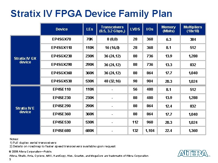
Stratix IV FPGA Device Family Plan Stratix IV GX device Device LEs Transceivers (8. 5, 3. 2 Gbps 1) LVDS I/Os Memory (Mbits) Multipliers (18 x 18) EP 4 SGX 70 70 K 8 (8, 0) 28 368 6. 3 384 EP 4 SGX 110 K 16 (16, 0) 28 368 8. 1 512 EP 4 SGX 230 K 36 (24, 12) 88 736 13. 9 1, 288 EP 4 SGX 290 K 36 (24, 12) 88 736 13. 3 832 EP 4 SGX 360 K 36 (24, 12) 88 864 17. 7 1, 040 EP 4 SGX 530 K 48 (32, 16) 98 904 20. 3 1, 024 EP 4 SE 110 K - 56 480 8. 1 512 EP 4 SE 230 K - 88 480 13. 9 1, 288 EP 4 SE 290 K - 88 864 12. 4 832 EP 4 SE 360 K - 88 864 17. 7 1, 040 EP 4 SE 530 K - 112 960 20. 3 1, 024 EP 4 SE 680 K - 132 1, 104 22. 4 1, 360 Stratix IV E device Notes: 1) Full duplex serial transceivers 2) Details on roadmap to faster speed transceivers available upon request © 2008 Altera Corporation—Public Altera, Stratix, Arria, Cyclone, MAX, Hard. Copy, Nios, Quartus, and Mega. Core are trademarks of Altera Corporation 3

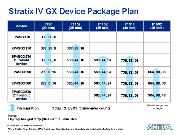
Stratix IV GX Device Package Plan Device F 780 (29 mm) F 1152 (35 mm) F 1517 (40 mm) EP 4 SGX 70 368, 28, 8 EP 4 SGX 110 368, 28, 8 368, 28, 16 EP 4 SGX 230 1 st rollout device 368, 28, 8 EP 4 SGX 290 EP 4 SGX 360 560, 44, 16 560, 44, 24 736, 88, 36 288, 0, 16 560, 44, 24 736, 88, 36 864, 88, 36 560, 44, 24 736, 88, 36 904, 98, 48 EP 4 SGX 530 2 nd rollout device Pin migration Total I/O, LVDS, transceiver counts Notes: Flip. Chip ball-grid array (BGA) with 1. 0 -mm pitch © 2008 Altera Corporation—Public Altera, Stratix, Arria, Cyclone, MAX, Hard. Copy, Nios, Quartus, and Mega. Core are trademarks of Altera Corporation 4 F 1932 (45 mm) Details subject to change

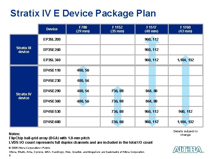
Stratix IV E Device Package Plan Device Stratix III device Stratix IV device F 780 (29 mm) F 1152 (35 mm) F 1517 (40 mm) EP 3 SL 200 960, 112 EP 3 SE 260 960, 112 EP 3 SL 340 960, 112 F 1760 (43 mm) 1, 104, 132 EP 4 SE 110 480, 56 EP 4 SE 230 480, 56 EP 4 SE 290 480, 56 736, 88 864, 88 EP 4 SE 360 480, 56 736, 88 864, 88 EP 4 SE 530 736, 88 960, 112 EP 4 SE 680 736, 88 960, 112 1, 104, 132 Notes: Flip. Chip ball-grid array (BGA) with 1. 0 -mm pitch LVDS I/O count represents full duplex channels and are included in the total I/O count © 2008 Altera Corporation—Public Altera, Stratix, Arria, Cyclone, MAX, Hard. Copy, Nios, Quartus, and Mega. Core are trademarks of Altera Corporation 5 Details subject to change

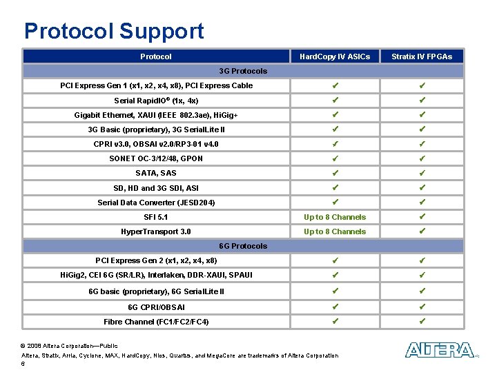
Protocol Support Protocol Hard. Copy IV ASICs Stratix IV FPGAs PCI Express Gen 1 (x 1, x 2, x 4, x 8), PCI Express Cable Serial Rapid. IO® (1 x, 4 x) Gigabit Ethernet, XAUI (IEEE 802. 3 ae), Hi. Gig+ 3 G Basic (proprietary), 3 G Serial. Lite II CPRI v 3. 0, OBSAI v 2. 0/RP 3 -01 v 4. 0 SONET OC-3/12/48, GPON SATA, SAS SD, HD and 3 G SDI, ASI Serial Data Converter (JESD 204) SFI 5. 1 Up to 8 Channels Hyper. Transport 3. 0 Up to 8 Channels PCI Express Gen 2 (x 1, x 2, x 4, x 8) Hi. Gig 2, CEI 6 G (SR/LR), Interlaken, DDR-XAUI, SPAUI 6 G basic (proprietary), 6 G Serial. Lite II 6 G CPRI/OBSAI Fibre Channel (FC 1/FC 2/FC 4) 3 G Protocols 6 G Protocols © 2008 Altera Corporation—Public Altera, Stratix, Arria, Cyclone, MAX, Hard. Copy, Nios, Quartus, and Mega. Core are trademarks of Altera Corporation 6

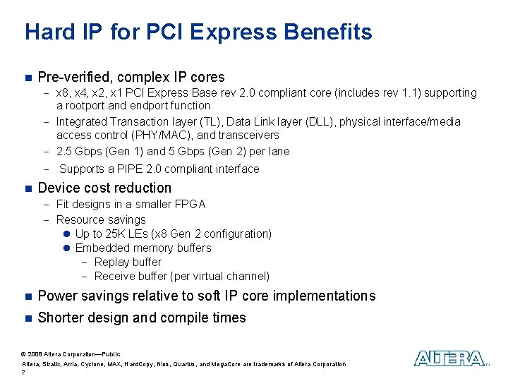
Hard IP for PCI Express Benefits n Pre-verified, complex IP cores - x 8, x 4, x 2, x 1 PCI Express Base rev 2. 0 compliant core (includes rev 1. 1) supporting a rootport and endport function - Integrated Transaction layer (TL), Data Link layer (DLL), physical interface/media access control (PHY/MAC), and transceivers - 2. 5 Gbps (Gen 1) and 5 Gbps (Gen 2) per lane - Supports a PIPE 2. 0 compliant interface n Device cost reduction - Fit designs in a smaller FPGA - Resource savings l Up to 25 K LEs (x 8 Gen 2 configuration) l Embedded memory buffers - Replay buffer - Receive buffer (per virtual channel) n Power savings relative to soft IP core implementations n Shorter design and compile times © 2008 Altera Corporation—Public Altera, Stratix, Arria, Cyclone, MAX, Hard. Copy, Nios, Quartus, and Mega. Core are trademarks of Altera Corporation 7

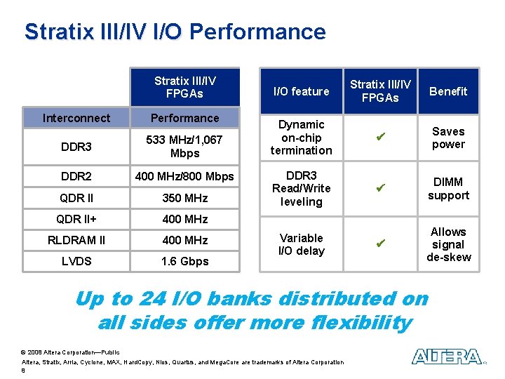
Stratix III/IV I/O Performance Stratix III/IV FPGAs Interconnect Performance DDR 3 533 MHz/1, 067 Mbps DDR 2 400 MHz/800 Mbps QDR II 350 MHz QDR II+ 400 MHz RLDRAM II 400 MHz LVDS 1. 6 Gbps I/O feature Stratix III/IV FPGAs Benefit Dynamic on-chip termination Saves power DDR 3 Read/Write leveling DIMM support Allows signal de-skew Variable I/O delay Up to 24 I/O banks distributed on all sides offer more flexibility © 2008 Altera Corporation—Public Altera, Stratix, Arria, Cyclone, MAX, Hard. Copy, Nios, Quartus, and Mega. Core are trademarks of Altera Corporation 8

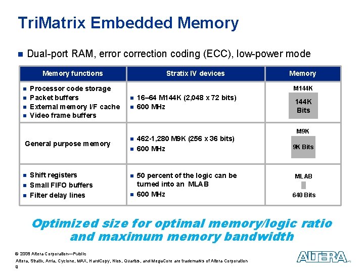
Tri. Matrix Embedded Memory n Dual-port RAM, error correction coding (ECC), low-power mode Memory functions n n Processor code storage Packet buffers External memory I/F cache Video frame buffers General purpose memory n n n Shift registers Small FIFO buffers Filter delay lines Stratix IV devices Memory M 144 K n n n 16– 64 M 144 K (2, 048 x 72 bits) 600 MHz 462 -1, 280 M 9 K (256 x 36 bits) 600 MHz 50 percent of the logic can be turned into an MLAB 600 MHz 144 K Bits M 9 K 9 K Bits MLAB 640 Bits Optimized size for optimal memory/logic ratio and maximum memory bandwidth © 2008 Altera Corporation—Public Altera, Stratix, Arria, Cyclone, MAX, Hard. Copy, Nios, Quartus, and Mega. Core are trademarks of Altera Corporation 9

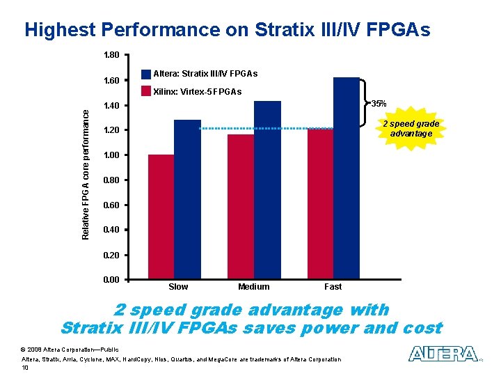
Highest Performance on Stratix III/IV FPGAs 1. 80 1. 60 Altera: Stratix III/IV FPGAs Relative FPGA core performance Xilinx: Virtex-5 FPGAs 35% 1. 40 2 speed grade advantage 1. 20 1. 00 0. 80 0. 60 0. 40 0. 20 0. 00 Slow Medium Fast 2 speed grade advantage with Stratix III/IV FPGAs saves power and cost © 2008 Altera Corporation—Public Altera, Stratix, Arria, Cyclone, MAX, Hard. Copy, Nios, Quartus, and Mega. Core are trademarks of Altera Corporation 10

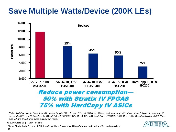
Save Multiple Watts/Device (200 K LEs) 14. 000 Devices 12. 000 Power (W) 10. 000 29% 8. 000 45% 6. 000 50% 75% 4. 000 2. 000 0. 000 Virtex-5, 1. 0 V V 5 -LX 220 Stratix III, 1. 1 V EP 3 SL 200 Stratix III, 0. 9 V EP 3 SL 200 Stratix IV, 0. 9 V EP 4 SE 230 Hard. Copy IV, 0. 9 V HC 230 Reduce power consumption— 50% with Stratix IV FPGAS 75% with Hard. Copy IV ASICs Note: Total power is based on 60 percent logic (ALUTs and FFs) at 200 MHz, 25 percent memory utilization of each type of memory, 50 percent DSP 18 x 18 block, 64 in/64 out 1. 8 -V LVCMOS (200 MHz), 128 in/128 out 2. 5 -V LVCMOS (200 MHz), 32 in/32 out (LVDS at 800 MHz), and 72 -pin DDR 3 interface power savings. © 2008 Altera Corporation—Public Altera, Stratix, Arria, Cyclone, MAX, Hard. Copy, Nios, Quartus, and Mega. Core are trademarks of Altera Corporation 11

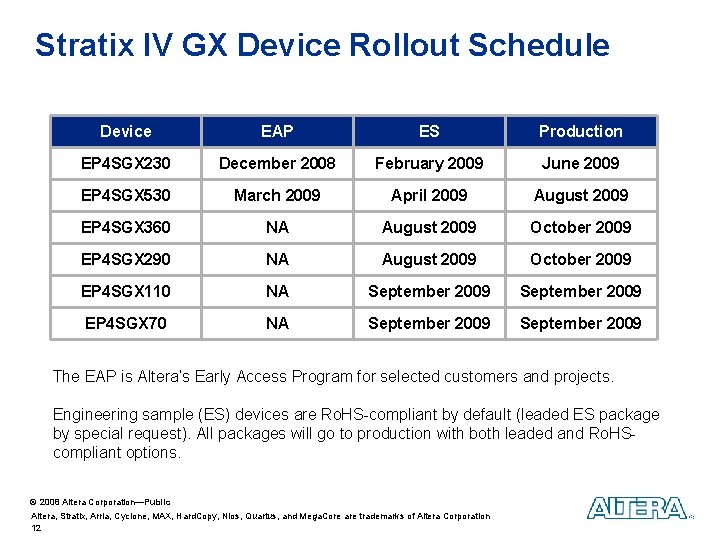
Stratix IV GX Device Rollout Schedule Device EAP ES Production EP 4 SGX 230 December 2008 February 2009 June 2009 EP 4 SGX 530 March 2009 April 2009 August 2009 EP 4 SGX 360 NA August 2009 October 2009 EP 4 SGX 290 NA August 2009 October 2009 EP 4 SGX 110 NA September 2009 EP 4 SGX 70 NA September 2009 The EAP is Altera’s Early Access Program for selected customers and projects. Engineering sample (ES) devices are Ro. HS-compliant by default (leaded ES package by special request). All packages will go to production with both leaded and Ro. HScompliant options. © 2008 Altera Corporation—Public Altera, Stratix, Arria, Cyclone, MAX, Hard. Copy, Nios, Quartus, and Mega. Core are trademarks of Altera Corporation 12