4 Combinational Logic Networks 4 2 Layout Design
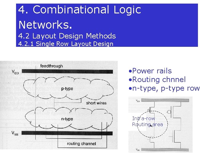
4. Combinational Logic Networks. 4. 2 Layout Design Methods 4. 2. 1 Single Row Layout Design • Power rails • Routing chnnel • n-type, p-type row Intra-row Routing area

Structure of a routing channel • Horizontal tracks and vertical tracks • Channel Density, changed with pin assignment. (below)
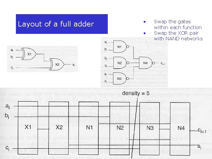
Layout of a full adder • • Swap the gates within each function Swap the XOR pair with NAND networks

Left-edge channel routing • Optimum under assumption that only one horizontal wire segment per net. Channel that cannot be routed by the left edge algorithm (Vertical constraint) A dogleg wire
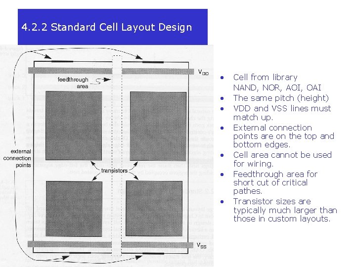
4. 2. 2 Standard Cell Layout Design • • Cell from library NAND, NOR, AOI, OAI The same pitch (height) VDD and VSS lines must match up. External connection points are on the top and bottom edges. Cell area cannot be used for wiring. Feedthrough area for short cut of critical pathes. Transistor sizes are typically much larger than those in custom layouts.
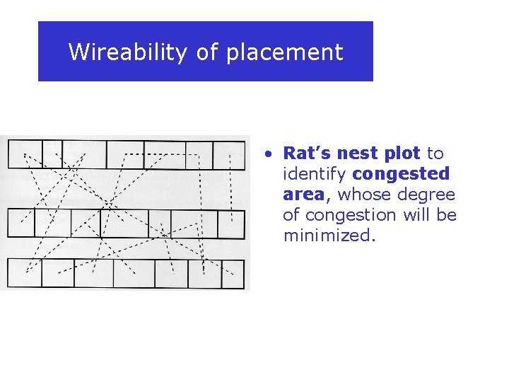
Wireability of placement • Rat’s nest plot to identify congested area, whose degree of congestion will be minimized.

4. 3 Simulation • Circuit Simulation • Timing Simulation • Switch Simulation • Gate Simulation (Logic Simulation) Propagate new value until it will be stable a 1 b 0 b 1 c c 0 0 d 1 o o 1 0
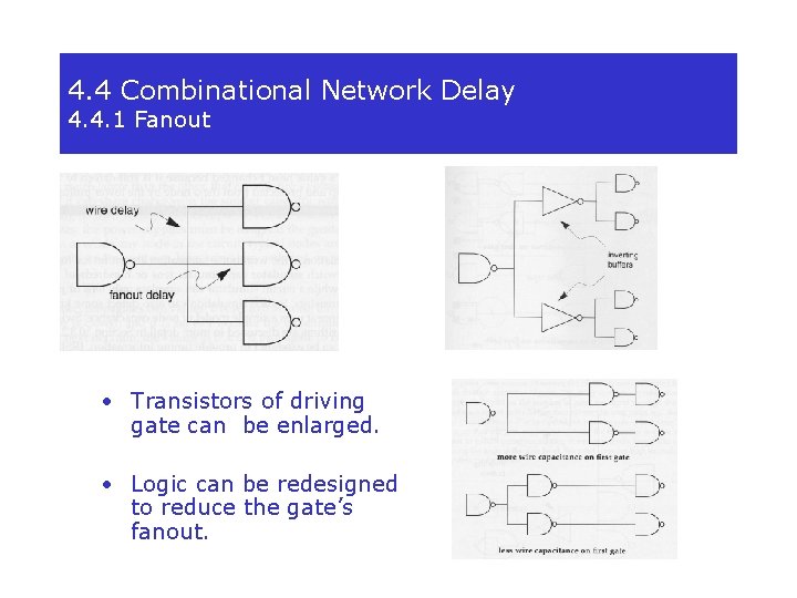
4. 4 Combinational Network Delay 4. 4. 1 Fanout • Transistors of driving gate can be enlarged. • Logic can be redesigned to reduce the gate’s fanout.
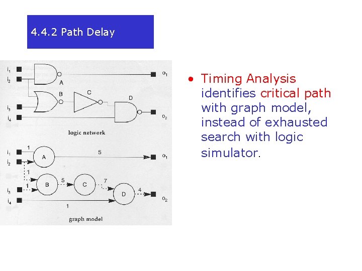
4. 4. 2 Path Delay • Timing Analysis identifies critical path with graph model, instead of exhausted search with logic simulator.
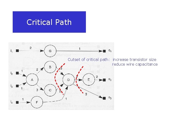
Critical Path Cutset of critical path: increase transistor size reduce wire capacitance
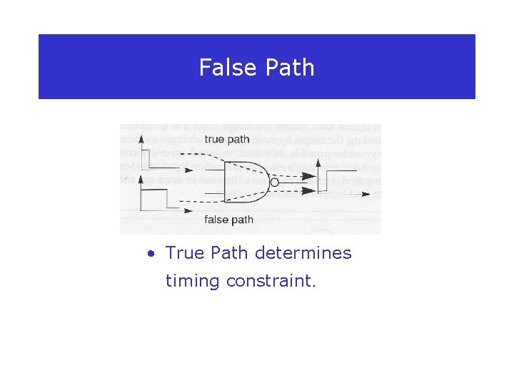
False Path • True Path determines timing constraint.
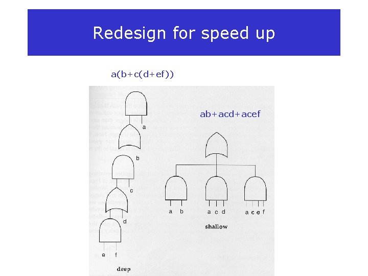
Redesign for speed up a(b+c(d+ef)) ab+acd+acef
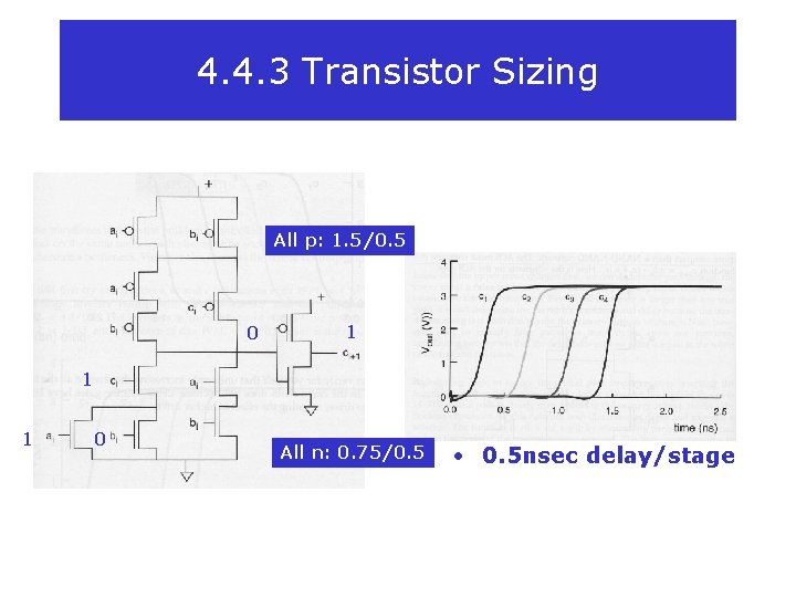
4. 4. 3 Transistor Sizing All p: 1. 5/0. 5 0 1 1 1 0 All n: 0. 75/0. 5 • 0. 5 nsec delay/stage
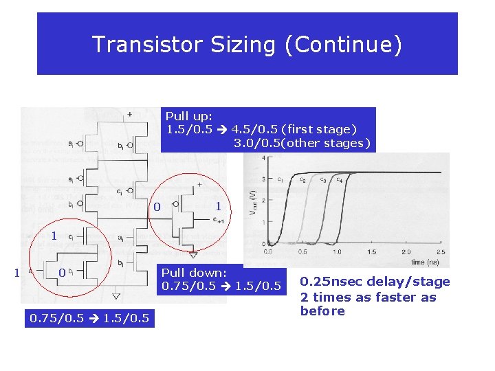
Transistor Sizing (Continue) Pull up: 1. 5/0. 5 4. 5/0. 5 (first stage) 3. 0/0. 5(other stages) 0 1 1 1 0 0. 75/0. 5 1. 5/0. 5 Pull down: 0. 75/0. 5 1. 5/0. 5 • 0. 25 nsec delay/stage 2 times as faster as before
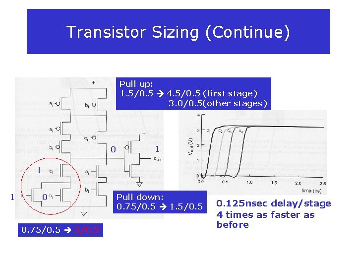
Transistor Sizing (Continue) Pull up: 1. 5/0. 5 4. 5/0. 5 (first stage) 3. 0/0. 5(other stages) 0 1 1 1 0 0. 75/0. 5 3/0. 5 Pull down: 0. 75/0. 5 1. 5/0. 5 • 0. 125 nsec delay/stage 4 times as faster as before
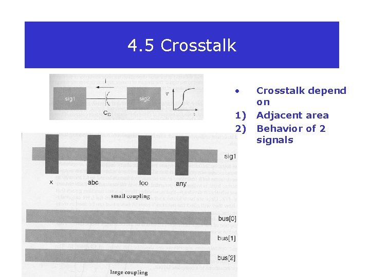
4. 5 Crosstalk • 1) 2) Crosstalk depend on Adjacent area Behavior of 2 signals
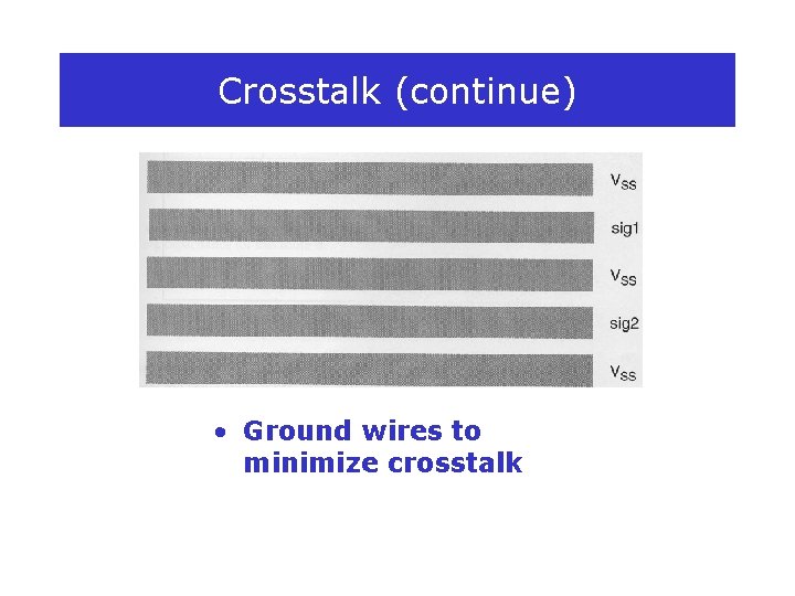
Crosstalk (continue) • Ground wires to minimize crosstalk
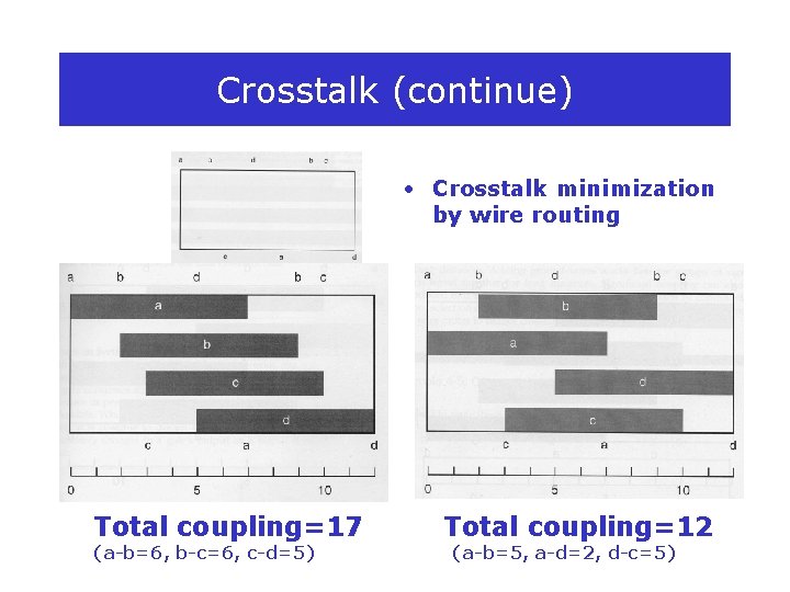
Crosstalk (continue) • Crosstalk minimization by wire routing Total coupling=17 (a-b=6, b-c=6, c-d=5) Total coupling=12 (a-b=5, a-d=2, d-c=5)
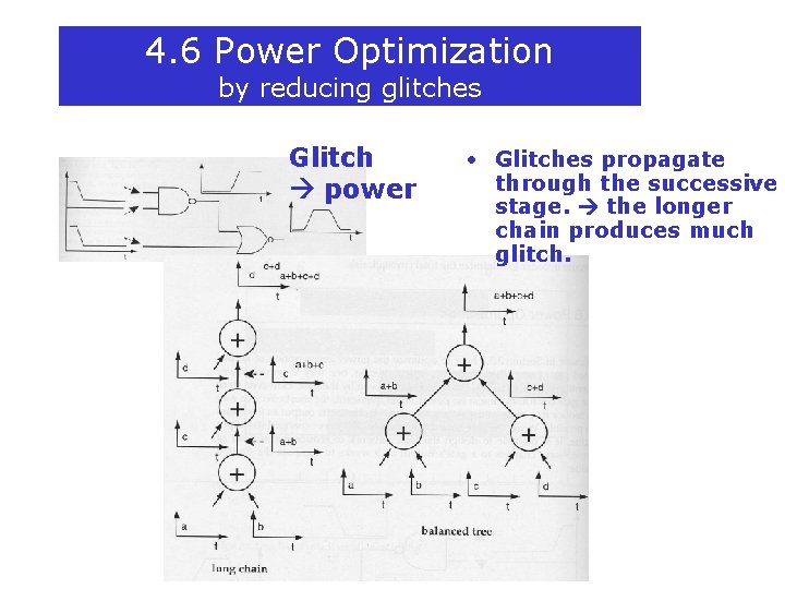
4. 6 Power Optimization by reducing glitches Glitch power • Glitches propagate through the successive stage. the longer chain produces much glitch.
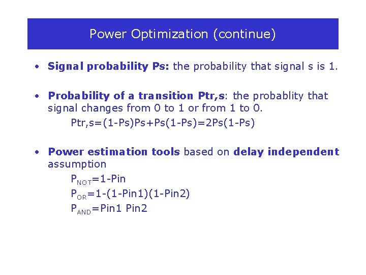
Power Optimization (continue) • Signal probability Ps: the probability that signal s is 1. • Probability of a transition Ptr, s: the probablity that signal changes from 0 to 1 or from 1 to 0. Ptr, s=(1 -Ps)Ps+Ps(1 -Ps)=2 Ps(1 -Ps) • Power estimation tools based on delay independent assumption PNOT=1 -Pin POR=1 -(1 -Pin 1)(1 -Pin 2) PAND=Pin 1 Pin 2
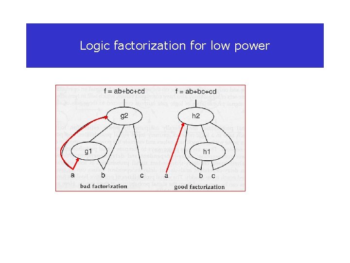
Logic factorization for low power
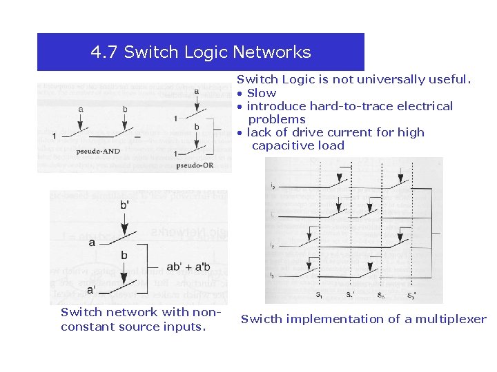
4. 7 Switch Logic Networks Switch Logic is not universally useful. • Slow • introduce hard-to-trace electrical problems • lack of drive current for high capacitive load Switch network with nonconstant source inputs. Swicth implementation of a multiplexer
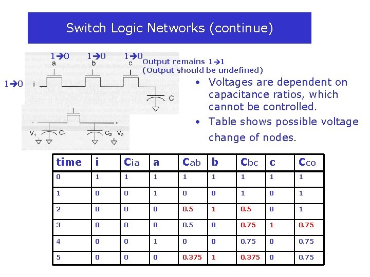
Switch Logic Networks (continue) 1 0 1 0 Output remains 1 1 (Output should be undefined) • Voltages are dependent on capacitance ratios, which cannot be controlled. • Table shows possible voltage 1 0 change of nodes. time i Cia a Cab b Cbc c Cco 0 1 1 1 1 1 0 0 1 0 1 2 0 0. 5 1 0. 5 0 1 3 0 0. 5 0 0. 75 1 0. 75 4 0 0 1 0 0 0. 75 5 0 0. 375 1 0. 375 0 0. 75
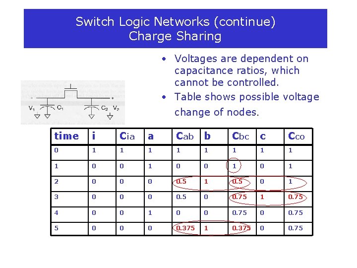
Switch Logic Networks (continue) Charge Sharing • Voltages are dependent on capacitance ratios, which cannot be controlled. • Table shows possible voltage change of nodes. time i Cia a Cab b Cbc c Cco 0 1 1 1 1 1 0 0 1 0 1 2 0 0. 5 1 0. 5 0 1 3 0 0. 5 0 0. 75 1 0. 75 4 0 0 1 0 0 0. 75 5 0 0. 375 1 0. 375 0 0. 75
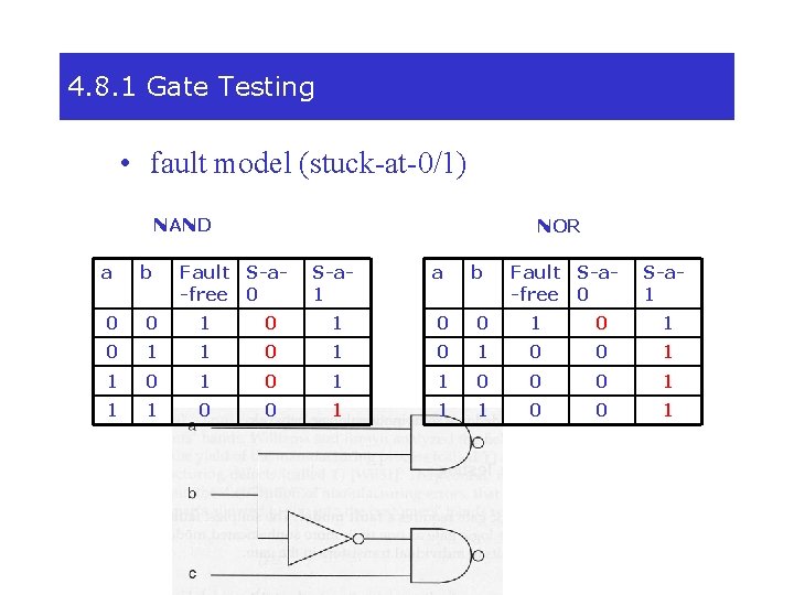
4. 8. 1 Gate Testing • fault model (stuck-at-0/1) NAND a b NOR Fault S-a-free 0 S-a 1 a b Fault S-a-free 0 S-a 1 0 0 1 0 1 0 0 1 1 0 0 0 1 1 1 0 0 1
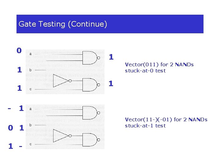
Gate Testing (Continue) 0 1 Vector(011) for 2 NANDs stuck-at-0 test 1 1 - 1 1 0 1 1 - Vector(11 -)(-01) for 2 NANDs stuck-at-1 test
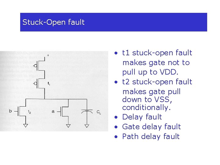
Stuck-Open fault • t 1 stuck-open fault makes gate not to pull up to VDD. • t 2 stuck-open fault makes gate pull down to VSS, conditionally. • Delay fault • Gate delay fault • Path delay fault
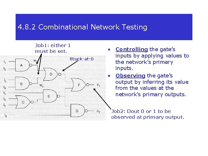
4. 8. 2 Combinational Network Testing Job 1: either 1 must be set. Stuck-at-0 • Controlling the gate’s inputs by applying values to the network’s primary inputs. • Observing the gate’s output by inferring its value from the values at the network’s primary outputs. Job 2: Dout 0 or 1 to be observed at primary output.
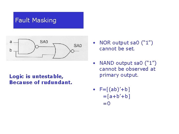
Fault Masking • NOR output sa 0 (“ 1”) cannot be set. Logic is untestable, Because of rudundant. • NAND output sa 0 (“ 1”) cannot be observed at primary output. • F=[(ab)’+b] =[a+b’+b] =0
- Slides: 29