4 Circuit Characterization Contents 1 Linear Circuit Components


 : V i v 1 C v 2 q Inductance(L) : V")
 Z(w) w. L 1) region")

 characteristics Load characteristics linear triode")
 demands i 1=i 2 VDD RL Vi")
 =")

 Static Load Line : i. L = i. D VDD ii) Dynamic Load")


2 i. D Vi=0")
 Eq.")
를 invert & integrate 한 curve dt C = d. V i eq(2) t")
 v -1 C eq. (2) D-load : 0.")
 정의) = 한 inverter가 같은 size의 연결된 inverter의 입력전압을 방전시")


 Gate capacitance off G non-sat. (short-channel) 0")
 24")
 Junction capacitance Sidewall junction is more abrupt 25")
 Overlap capacitance(due to lateral diffusion) 26")
 for SPICE 27")
 Routing Capacitance Csw Cf t Cp S Csw Cp: fringing cap. Csw: sidewall")


 C (Lumped) Vout Time elapsed D")


 (p = ,")
 MOSFET Configuration Penfield-Rubinstein model : C 4 A N 4 B N")

 50%-50% delay : for multiple levels of static logic circuit")
 10%-90%(90 -10) delay : rise time(fall time) : for precharged dynamic circuit 38")


 VTN + VTP < VDD-VSS : static current")

 dynamic power dissipation Vi Vi Substituting, Vo t=0 Vo and")
,")

 In Vo’s going down R R i lose 1/2 store 1/2 R lose")
 Short-circuit dissipation ref. H. J. M. Veendrick, “Short-circuit dissipation of static CMOS…” IEEE")


 PT=Pdyn+ PSC : input")
 Ring counter for measuring gate delay VDD i 1 C Cg i 1")

 – causes deformation,")


 59")

- Slides: 60
4 Circuit Characterization Contents 1. Linear Circuit Components ; R, L & C 2. Dominant Components in each w-region(delay, voltage drop) 3. inverter DC & delay characteristics 4. R & C Model for MOSFET’s & wires MOS(internal) device capacitance Diffusion(external device ; source/drain) capacitance Routing capacitance, resistance 5. Gate delay input slope series-connected(stacked) MOSFET configuration : Penfield-Rubinstein model inverter stage ratio 1
6. CMOS용 inverter & Power dissipation Static dynamic Short-circuit Ring counter 7. High-Current Effects Power/Ground bounce EM/ESD/EOS(Electro-migration/Electro-Static Discharge/Electrical Over. Stress) 2
1. Linear Circuit components : R, L & C v i. R q Resistance CR) : i R v V i=qv V Velocity Saturation t t : mean time between collision 3
q Capacitance(C) : V i v 1 C v 2 q Inductance(L) : V w. L i + v - i 4
2. Dominant components V=Z • i (z = impedance) Z(w) w. L 1) region I : C dominates 2) region II : R dominates R 3) region III : L dominates II I w wc III w. L 5
3. Inverter DC & delay characteristics 1 1 0 0 load 0 seesaw rope seesaw 2 foods seesaw balance rdendez-vous seesaw q Role of inverter : 1. Signal buffering/transmission 2. Logic function 6
q Inverter is composed of driver and load driver(transistor) characteristics Load characteristics linear triode VGS 4(8 V) i 1 i 2 VGS 3(6 V) VGS 2(4 V) VGS 1(2 V) VDS D G i 1 S out in V 12 1 i 2 RL 2 7
q Putting them together, KCL(Kirchoff’s Current Low) demands i 1=i 2 VDD RL Vi i i I= Vo (Vo-VDD) Vi Vo VDD <Output Characteristics> <Transfer Characteristics> Vo Ideal RL increase Vi 8
q Resistor, as a passive load, requires large silicon area. RL(10 K ) = 100 R (100 / ) Active load is better for digital purposes. VDD Large area (100 s) Vo Vi GND 9
q Problems with Enhancement load 1. Slow charge/discharge due to small load current especially when Vo VDD 2. Vo cannot be raised higher than VDD-VT’ (VT’ : threshold voltage considering body effect) Vi = 5 V Q 1 : Static load line Dynamic load line Q 2 A B Vi = 0 V VDD-VT VDD 10
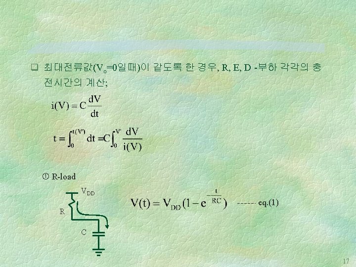
i) Static Load Line : i. L = i. D VDD ii) Dynamic Load Line(due to load capacitance, CL) i. L charging(Q 1 Q 2) ; Vo Vi i. D = i. L - CL discharging(Q 2 Q 1) ; i. D = i. L + Magnitude of average charging/discharging current is given as the area of AQ 1 Q 2 B 11
q How to improve Inverter speed is how to increase charge/discharge current. n Sol. 1. Bootstrap method VDD I Vi=5 V T 1 X T 2 Dynamic load line (due to CX) Vo CX Vi Q 1 T 3 Q 2 Q 3 Vi=0 V Static load line VDD-2 VT VDD VO 12
n Sol. 2 Depletion load method Depletion Enhancement ID element ID VTD<0 - VG=0 V VG=-1 V VTD>0 0 Depletion type VG=2 V VG=-2 V VG=2 V + VG VDD VG=1 V VG=0 V Enhance -ment type Question) Why cannot one use depletion MOSFET as a logic element ? 13
VDD i. L Vi Vo Vi=5 V i. D i. L=b(-VTD)2 i. D Vi=0 V VDD body 효과를 고려한 부하선 VDS(=V 0) q Gate and Source terminals of Depletion device is tied together to suppress the Vo-dependence of i. L, i. e. , i. L=b(0 -VTD)2= b VTD 2, acting like a constant current source. 14
q Speed comparison between R, E, D-load VDD i t=0 C Eq. (1) Eq. (2) VDD R D R i Eq. (3) VDD 0. 6 R D’ E Charging time vs. voltage 0. 8 VDD 15
eq(1)를 invert & integrate 한 curve dt C = d. V i eq(2) t dt d. V E R t 0 VDD+VTD=0. 4 VD eq(3) D’ VDD-VTE=0. 8 VD Output voltage, V 16
E-load : VDD i. E(v) v -1 C eq. (2) D-load : 0. 4 VDD<V<VDD에서는 0. 6 R의 저항을 통한 충전 : eq. (3) 18
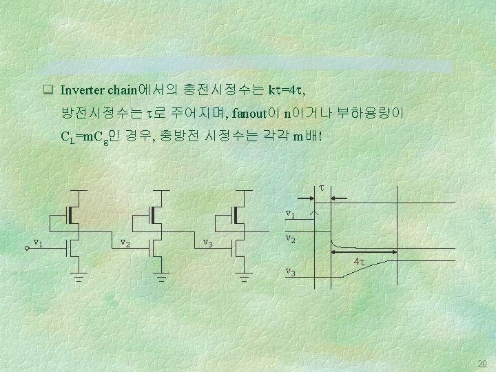
q Inverter delay( ) 정의) = 한 inverter가 같은 size의 연결된 inverter의 입력전압을 방전시 키는 시정수 SW 1 Cg RL RL k SW 2 RD Cg Cg RD Cg RL : depletion 소자 등가저항 RD : driver의 등가저항 ; inverter ratio = q inverter ratio k is determined as 4, from the following static consideration 19
q Effective load capacitance, CL = CS+ Cgs +2 Cgd >> Cg m. Cgd Cs Av: inverter 전압이득 m=1 -Av Cgs q Miller capacitance A DV Cgd B Av DV (1 -Av) DV ; effective voltage change Effective capacitance = Total charge change input voltage change Miller factor For digital inverter (1 -Av) => 2 21
4. R & C Models for MOSFET’s & wires Transistor as R 22
MOSFET Capacitance MOSFET: 4 -terminal device i) Gate capacitance off G non-sat. (short-channel) 0 0 CGB CGS CGD D S CDB CSB B CGS 0 CGD 0 CG(total) 0 CGB CG=CGS+CGD+CGB 2/3 CGS 0. 5 C [COX] CGD off sat. lin. CGB VGS 23
MOSFET parastic capacitance(=junction cap. +overlap cap. ) 24
ii) Junction capacitance Sidewall junction is more abrupt 25
iii) Overlap capacitance(due to lateral diffusion) 26
Capacitance, Conductance values(typical) for SPICE 27
iv) Routing Capacitance Csw Cf t Cp S Csw Cp: fringing cap. Csw: sidewall cap. W Cp: planar cap. Cp Assume t=const Cf W(=S) For high-(t/w), multi-bit bus, Csw dominates. 28
q Distributed RC line R Vj-1 R C Vj C R Vj+1 R C R = r dx (r: resistance per length) C = c dx(c: capacitance per length) : Diffusion equation (tx : time for propagating distance x) 29
q Frequency domain solution of the distributed RC line to unit step input is as cosh(x) = 30
q Distributed vs. Lumped R R C (Distributed) C (Lumped) Vout Time elapsed D L time Distributed Lumped 0 - 90% RC 2. 3 RC 0 - 63% 0. 5 RC RC 0 - 10% 0. 1 RC 31
q Characteristic of Diffusion : tx kx 2 t=1 t=4 t=9 t=16 0 1 2 3 1 mm 4 x 1 mm For t =4 10 -15 2[ in m] I) with buffer tp = 8 ns + buffer ii) without buffer tp = 16 ns 32
5. Gate Delay q t. T = t. D + ti + tslew, tslew = rslew CL t. D : internal delay of the cell ti = delay due to the intrinsic output capacitance rslew : output slew rate [ns/p. F] CL : load capacitance for each output input t. D output Ex. t. Q=1. 39+0. 83+1. 63 CL tslew ti t. D = t. D, O Kt Kv Kp KV Kt 3. 0 3. 3 3. 6 VDD -30 RT +90 process Kp Slow 1. 34 typ. 1. 00 fast 0. 72 33
q input slope dependence (n = , : input rise time) (p = , : input fall time) 34
q Series-connected(stacked) MOSFET Configuration Penfield-Rubinstein model : C 4 A N 4 B N 3 C N 2 C 2 D N 1 C 1 : Summed resistance from i to power/ground : Capacitance at point i td = R 1 C 1 + (R 1+R 2)C 2 + (R 1+R 2+R 3)C 3 + (R 1+R 2+R 3+R 4)C 4 = R 1(C 1+C 2+C 3+C 4) + R 2(C 2+C 3+C 4)+R 3(C 3+C 4)+R 4 C 4 Elmore delay model 35
q Elmore delay TAB = R 1(C 2+C 3+C 4 +C 5 +C 6 +C 7 +C 8 +C 9 +C 10) +R 2( +C 3+C 4 +C 5 + C 6 +C 7 +C 8 +C 9 +C 10 ) +R 3( +C 4 +C 5 + C 6 +C 7 +C 8 +C 9 +C 10) TBD = R 4( +R 7( +C 7 +C 8 +C 9) TBE = R 5( +R 6( +C 6 +C 10) 36
q Delay Modelling i) 50%-50% delay : for multiple levels of static logic circuit 37
ii) 10%-90%(90 -10) delay : rise time(fall time) : for precharged dynamic circuit 38
q Delay model of interconnection driven by Rtr & terminated by CL Rtr Rint Cint T 90% = 1. 0 Rint Cint + 2. 3(Rtr. Cint+ Rtr. CL+ Rint. CL) CL 39
q Inverter Stage Ration Driving large C load using graded inverter chain 1 f f 2 f. N Cg CL Q. Determine the scale-up factor, f minimizing total delay time for driving CL from Cg 40
A. mumber of inverters, N is given by = Y, i. e. , N= Total delay is Nf , which is to be minimized. Total delay = = * In real situation, f could be much larger than 2. 7 to reduce the chip area consumption 41
6. CMOS Inverter & Power Dissipation VDD G S q Static Transfer Characterictic D Vi I G D S C VDD A B D E Vo 0 VTN VDD 2 VDD V i VDD- VTD PMOS Vo NMOS (VSS or GND) NMOS PMOS Region A cutoff linear Region B sat linear Region C sat Region D linear sat Region E linear cutoff Static power dissipation 42
q Adjustment of VTN, VTP i) VTN + VTP < VDD-VSS : static current flows ii) VTN + VTP = VDD-VSS : ideal case iii) VTN + VTP > VDD-VSS : hysteresis PMOS VTN 0 VTN NMOS Vi VTP V DD Both are off Vi VDD-VTP Vo Vo Vo Vi 43
q Influence of PN asymmetry on the transfer characteristics Vo 10 0. 1 Vi VDD infinite transfer gain ideal zero output conductance 44
q Power Consumption i) dynamic power dissipation Vi Vi Substituting, Vo t=0 Vo and (f : switching frequency) eq. (1. 11) 45
q Energy stored in CL charged up to VDD is from eq. (1. 11), switching energy consumed per cycle is where did go ? 46
q Modelling of resistive dissipation in ideal switch replace MOSFET by ideal switch in serial with a resistance, R i) In Vo’s going up ; R i Vo (indep. of R!) ; energy dissipated R in R as Vo is being raised from 0 to VDD 47
ii) In Vo’s going down R R i lose 1/2 store 1/2 R lose 1/2 Energy dissipated in R as CL is being discharged GND 48
iii) Short-circuit dissipation ref. H. J. M. Veendrick, “Short-circuit dissipation of static CMOS…” IEEE J. Solid-state Circuits, Vol. SC-19, Aug, 1984. Pp 468 -473 assumption: CL = 0 Vi VDD T r f VDD-|VTP| VDD/2 VTN Vi i Vo i imax (A) (B) iav t=0 t 1 t 2 t 3 49
q For simplicity, assume , t = tr = tf and VT = VTN = -VTP (waveform (A) = waveform(B), (A) is symmetric w. r. t t = t 2 ) setting 50
Short-circuit current waveform with finite CL obtained from SPICE CL=0 200 A CL=200 f. F=2 x 10 -13 F CL=500 f. F ISC CL=1 p. F CL= 0. 8 VDD - |VTP| 2 3 4 CL 5 time(nsec) = n= p=170 A/V 2 Vt=Vtn=|Vtp|=0. 8 V VTN time(nsec) 51
output voltage CL=1 p. F CL=0 CL=500 f. F time(nsec) PT=Pdyn+ PSC : input voltage rise time =20 ns ln PT =10 ns total dissipation(PT) =5 ns For a load capacitance C*, = 5 ns in near optimal input transient =1 ns dynamic dissipation limit ln C* ln CL Pdyn PSC (sec) 52
C) Ring counter for measuring gate delay VDD i 1 C Cg i 1 d V 1 i 2 C i 3 C V 2 i 2 d i 3 d V 3 i 4 C i 4 d V 4 i 5 C V 5 VO i 5 d I 53
g i 1 C i 2 C i 3 C i 4 C i 5 C T g = T / N i 1 d i 2 d i 3 d i 4 d i 5 d 2 g Total discharge current at I-meter Power-delay product per gate =energy consumption per switching=QVDD=Cg. VDD 2=(VDDIDCT/N)*2 54
7. High-current Effects q Electro-migration: directional movement of charge carriers(DC current) – causes deformation, breakage of conductor, occurs at the constriction point. – ex) fuse(positive use of EM effect) depending on current density, temperature, and crystal structure limiting current: 2 m. A/ m 2 – rule of thumb: use 0. 4 -1. 0 m. A/ m 2 for VDD & VSS 55
q Power & Ground Bounce temporary level change in the power and ground voltage due to sudden change of charging/discharging current called simultaneous switching noise, DI-noise, d. I/dt noise due to i. R and/or L di/dt drop in the power/ground rail originates from large current drivers such as clocking buffer, I/O buffer 56
q Power-distribution path in IC and the electrical model 57
q Simplified electrical model of a CMOS chip 58
8. Technology scaling(Constant E-field scaling) 59